

 Product
 Brand
Brand Articles
 Tools
Tools
Designing with PCA9306: Datasheet, Pinout, and I2C Level Translation Guide

Surface Mount Tape & Reel (TR) Voltage Translators & Level Shifters 1 Voltage Level 8-VFSOP (0.091, 2.30mm Width) Active 7 Weeks Weeks 1 (Unlimited)


Surface Mount Tape & Reel (TR) Voltage Translators & Level Shifters 1 Voltage Level 8-VFSOP (0.091, 2.30mm Width) Active 7 Weeks Weeks 1 (Unlimited)
Explore the PCA9306 dual bidirectional I2C voltage translator by NXP. Access datasheets, pinouts, and design tips for bridging 1.0V to 5V mixed-voltage systems.
- Executive Summary: What is the PCA9306?
- 1. Technical Specifications & Performance Analysis
- 2. Pinout, Package, and Configuration
- 3. Design & Integration Guide (For Engineers & Makers)
- 4. Typical Applications & Use Cases
- 5. Alternatives and Cross-Reference Guide
- 6. Frequently Asked Questions (FAQ)
- 7. Datasheets & Resources
- Specifications
- Parts with Similar Specs
- Datasheet PDF
Executive Summary: What is the PCA9306?
The PCA9306 is a dual bidirectional I2C-bus and SMBus voltage-level translator designed for seamless communication between mixed-voltage processors and peripherals typically found in mobile devices and consumer electronics. As a standard logic component, it relies on a pass-transistor architecture to shift voltage levels without requiring a direction control pin. - Market Position: A high-volume, cost-effective commodity part essential for mixed-voltage BOMs (Bills of Materials).
Top Features:
Bidirectional Logic: Translates signals without a dedicated direction pin (auto-direction sensing via passive architecture).
Voltage Range: Supports translation between 1.0 V and 5.0 V.
Performance: Low 3.5 $\Omega$ ON-state resistance and < 1.5 ns propagation delay.
Primary Audience: Embedded Systems Engineers, IoT Designers, and Procurement Managers seeking drop-in logic replacements.
Supply Status: Active (widely available from NXP, TI, and Nexperia).
1. Technical Specifications & Performance Analysis
1.1 Core Architecture (Pass-Gate Logic)
The PCA9306 utilizes a passive N-channel MOSFET architecture rather than active buffering. This means the device acts as a switch: when the input is low, the switch is closed, connecting the two buses; when the input is high, the switch opens, and external pull-up resistors pull the respective buses to their voltage rails. This design eliminates the need for a DIR (Direction) pin, reducing control overhead for the CPU.
1.2 Key Electrical Characteristics
For design feasibility, engineers must strictly adhere to the voltage differential rules to ensure the internal FETs bias correctly. - Vref(1) (Low-Voltage Side): Operational from 1.0 V to 3.6 V.
Vref(2) (High-Voltage Side): Operational from 1.8 V to 5.5 V.
Propagation Delay: Maximum of 1.5 ns (ideal for standard and fast-mode I2C).
ON-State Resistance ($R_{on}$): Typical 3.5 $\Omega$.
Standby Current: Extremely low due to passive nature, making it suitable for battery-powered applications.
Critical Design Constraint: The Enable (EN) pin and Vref(2) must typically be at least 0.6 V higher than Vref(1) to bias the pass transistor effectively.
1.3 Interfaces and Connectivity
The unique value of the PCA9306 is its "open-drain" compatibility, making it the industry standard for:
Primary Buses: I2C, SMBus, and PMBus.
Other Protocols: MDIO (Management Data Input/Output), UART (Tx/Rx only), and GPIO shifting.
Mixed-Mode Support: Its 5 V tolerant I/O allows modern 1.8 V MCUs to talk to legacy 5 V sensors safely.
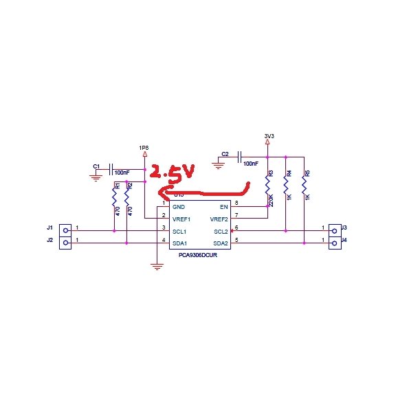
PCA9306 functional block diagram
2. Pinout, Package, and Configuration
2.1 Pin Configuration Guide
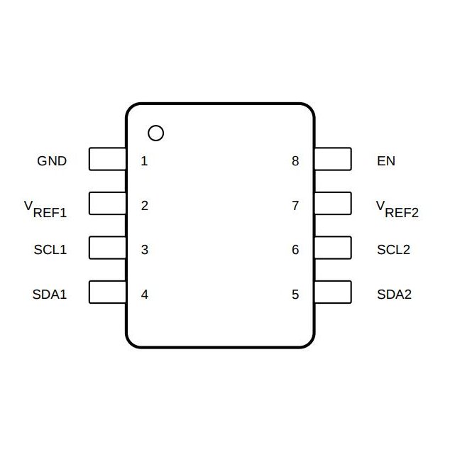
PCA9306 pinout diagram
The PCA9306 is an 8-pin device. The pinout is symmetrical in nature to facilitate easy PCB routing. - Pins 1 & 8 (GND / EN): Ground reference and Enable pin (Active High).
Pins 2 & 7 (VREF1 / VREF2): Supply voltages. VREF1 is for the lower voltage side; VREF2 is for the higher voltage side.
Pins 3 & 4 (SCL1 / SDA1): Low-voltage side bus connections.
Pins 5 & 6 (SDA2 / SCL2): High-voltage side bus connections.
2.2 Naming Convention & Ordering Codes
Understanding Part Numbers:The suffix following "PCA9306" indicates the physical package. Procurement teams must verify these codes to avoid receiving incompatible reels. * DC: VSSOP (Very Thin Shrink Small Outline) * DP: TSSOP (Thin Shrink Small Outline) * GF/GM/GU: Ultra-small leadless packages (XSON/XQFN) for mobile/space-constrained designs.
2.3 Available Packages
| Package Type | Dimensions (Approx) | Common Use Case |
|---|---|---|
| PCA9306DP (TSSOP8) | 3.0mm x 3.0mm (Lead pitch 0.65mm) | General Industrial, Hand-soldering friendly |
| PCA9306DC (VSSOP8) | 2.0mm x 2.3mm (Lead pitch 0.50mm) | Consumer Electronics, Compact PCBs |
| PCA9306GF (XSON8) | 1.35mm x 1.0mm | Mobile Phones, Wearables (Machine assembly only) |
3. Design & Integration Guide (For Engineers & Makers)
Pro Tip: Since the PCA9306 is a passive switch, it does not increase signal drive strength. Your pull-up resistors must be calculated to handle the total bus capacitance.
3.1 Hardware Implementation
Bypass Capacitors: Place a 0.1 µF ceramic capacitor close to the VREF2 pin to filter noise.
Pull-Up Resistors: Mandatory on both sides (Side 1 and Side 2). Values typically range from 2.2k$\Omega$ to 10k$\Omega$ depending on I2C speed (Standard vs. Fast Mode).
PCB Layout: Keep traces short to minimize capacitance. Ensure VREF2 is connected to the Enable pin through a 200k$\Omega$ resistor if controlled directly by the high-voltage rail.
3.2 Common Design Challenges
Below are resolutions to frequent "Pain Points" encountered during integration:
Passive Switch Limitations (Signal Integrity)
Issue: The device does not re-drive the signal. Long cables or high capacitance can degrade edge rates.
Fix: Carefully calculate pull-up resistor values. If bus capacitance exceeds 400pF, use an active buffer/repeater like the PCA9517 instead.
Voltage Differential Requirement
Issue: Translation fails if voltages are too close (e.g., 3.3V to 3.3V isolation or 2.5V to 3.0V).
Fix: Ensure Vref(2) $\ge$ Vref(1) + 0.6 V. This bias is critical for the internal isolation FETs.
Cumulative ON-Resistance
Issue: Putting multiple PCA9306 units in series adds to the trace resistance ($R_{on}$ approx 3.5 $\Omega$ per chip).
Fix: Avoid cascading more than two devices. The added resistance raises the $V_{OL}$ (Voltage Output Low) level, which might not be read as a "Legal Low" by the target CPU.
4. Typical Applications & Use Cases
📺 Video Recommendation: PCA9306 Guide
4.1 Real-World Example: IoT Smart Sensor Hub
In a typical smart home thermostat, a modern, low-power microcontroller (MCU) operating at 1.8 V needs to communicate with a legacy 5V humidity sensor.
The Problem: Direct connection would fry the MCU's I/O pins.
The PCA9306 Solution: - VREF1 connects to the MCU's 1.8 V rail. - VREF2 connects to the Sensor's 5.0 V rail. - The PCA9306 bridges the I2C command signals transparently. - When the 1.8 V MCU pulls SDA low, the PCA9306 pulls the 5 V side low instantly.
5. Alternatives and Cross-Reference Guide
The PCA9306 is an industry-standard footprint. Several manufacturers produce pin-compatible versions, offering procurement flexibility.
Direct Replacements (Pin-Compatible):
Texas Instruments PCA9306: Identical functionality and pinout. Often used interchangeably in BOMs.
Nexperia PCA9306: Common in high-volume distribution.
Diodes Inc PI4ULS3V08: Functional equivalent for varying voltage needs.
Active Buffer Alternatives (Better Performance):
TCA9517 / PCA9517: Use these if you need to drive long cables or isolate bus capacitance (Active Repeater).
Cost-Effective Options:
Analog Devices ADG3302: Check constraints; meant for general level translation but often pricier than the commodity PCA9306.
6. Frequently Asked Questions (FAQ)
Q: What is the difference between PCA9306 and PCA9517?
A: The PCA9306 is a passive switch (cheaper, faster, no drive), while the PCA9517 is an active buffer (reshapes signals, separates capacitance).
Q: Can PCA9306 be used for SPI level translation?
A: Yes, but only for bidirectional lines or open-drain setups. For standard push-pull SPI (MOSI/MISO), uni-directional buffers are often simpler, though PCA9306 works if pull-ups are added.
Q: Is the PCA9306 suitable for automotive applications?
A: Standard commercial versions are not. Look for "Q100" or automotive-grade suffixes (e.g., PCA9306-Q100) from manufacturers if full AEC-Q100 compliance is required.
Q: Does the PCA9306 require a directional control pin?
A: No. It uses an auto-sensing pass-gate architecture, making it ideal for the bidirectional data lines of I2C.
Q: What happens if Vref(2) is less than Vref(1)?
A: The device will not function correctly. Vref(2) must be the higher voltage potential to bias the internal transistors.
7. Datasheets & Resources
Official Datasheet: PCA9306 Data Sheet (NXP/TI/Nexperia)
Development Tools: Look for "I2C Level Shifter Breakout Board" (generic keyword).
Specifications
Parts with Similar Specs
- ImagePart NumberManufacturerPackage / CaseNumber of TerminationsMoisture Sensitivity Level (MSL)Translator TypePart StatusNumber of CircuitsPin CountRoHS StatusView Compare
![PCA9306DC1/DG,125]()
PCA9306DC1/DG,125
8-VFSOP (0.091, 2.30mm Width)
8
1 (Unlimited)
Voltage Level
Active
1
8
ROHS3 Compliant
![TCA9517DGKR]()
8-TSSOP, 8-MSOP (0.118, 3.00mm Width)
8
1 (Unlimited)
Voltage Level
Active
1
8
ROHS3 Compliant
![TCA9406DCUR]()
8-VFSOP (0.091, 2.30mm Width)
8
1 (Unlimited)
Voltage Level
Active
1
8
ROHS3 Compliant
![PCA9306IDCURQ1]()
8-VFSOP (0.091, 2.30mm Width)
8
1 (Unlimited)
Voltage Level
Active
1
8
ROHS3 Compliant


Datasheet PDF
- Datasheets :
- Environmental Information :
 TLV431 Programmable Reference Voltage: Specification, Pinout and Datasheet
16 August 20243979
 Unveiling the Intel 8XC251SA/SB/SP/SQ Microcontroller: Architectural Insights and System Details
29 February 2024276
 STM32F56x/76x: Comprehensive Technical Overview
29 February 2024365
 STM32G030F6P6: Overview, Features, Applications
19 October 20234995
 2SC5200 vs.TTC5200
08 July 202214925
 AD7878BQ Converter:Pinout, Specification, Datasheet
28 May 2021544
![LM317 Voltage Regulator[Video+FAQ]: Pinout, Circuit, LM317 VS LM7805 and Datasheet](https://res.utmel.com/Images/Article/1d33c68c-5ca5-4e96-a14d-1f10a89d8866.jpg) LM317 Voltage Regulator[Video+FAQ]: Pinout, Circuit, LM317 VS LM7805 and Datasheet
LM317 Voltage Regulator[Video+FAQ]: Pinout, Circuit, LM317 VS LM7805 and Datasheet27 April 202215430
 ADSP-21489BSWZ-4B vs ADSP-BF514KSWZ-4: Choosing the Right DSP
09 June 2025708
 What are Types and Application of Gas Sensors?
18 November 202511221
 What is a Memory Controller?
12 August 202035207
 Amorphous Silicon Solar Cells: Features, Structure and Applications
22 August 20226918
 Google Co-releases SayCan Model for Bots to Give Sensible Answers
30 August 20223966
 What are Proximity Sensors?
24 October 20258896
 The Introduction to Common Tools and Using Methods of Fiber Optic
07 January 20227477
 Global Power Technology Authorized Distributor | UTMEL Electronics
21 November 20234368
 How to Decide Which Relay Socket Is Right for Your Next Build
10 July 20253093
NXP USA Inc.
In Stock
United States
China
Canada
Japan
Russia
Germany
United Kingdom
Singapore
Italy
Hong Kong(China)
Taiwan(China)
France
Korea
Mexico
Netherlands
Malaysia
Austria
Spain
Switzerland
Poland
Thailand
Vietnam
India
United Arab Emirates
Afghanistan
Åland Islands
Albania
Algeria
American Samoa
Andorra
Angola
Anguilla
Antigua & Barbuda
Argentina
Armenia
Aruba
Australia
Azerbaijan
Bahamas
Bahrain
Bangladesh
Barbados
Belarus
Belgium
Belize
Benin
Bermuda
Bhutan
Bolivia
Bonaire, Sint Eustatius and Saba
Bosnia & Herzegovina
Botswana
Brazil
British Indian Ocean Territory
British Virgin Islands
Brunei
Bulgaria
Burkina Faso
Burundi
Cabo Verde
Cambodia
Cameroon
Cayman Islands
Central African Republic
Chad
Chile
Christmas Island
Cocos (Keeling) Islands
Colombia
Comoros
Congo
Congo (DRC)
Cook Islands
Costa Rica
Côte d’Ivoire
Croatia
Cuba
Curaçao
Cyprus
Czechia
Denmark
Djibouti
Dominica
Dominican Republic
Ecuador
Egypt
El Salvador
Equatorial Guinea
Eritrea
Estonia
Eswatini
Ethiopia
Falkland Islands
Faroe Islands
Fiji
Finland
French Guiana
French Polynesia
Gabon
Gambia
Georgia
Ghana
Gibraltar
Greece
Greenland
Grenada
Guadeloupe
Guam
Guatemala
Guernsey
Guinea
Guinea-Bissau
Guyana
Haiti
Honduras
Hungary
Iceland
Indonesia
Iran
Iraq
Ireland
Isle of Man
Israel
Jamaica
Jersey
Jordan
Kazakhstan
Kenya
Kiribati
Kosovo
Kuwait
Kyrgyzstan
Laos
Latvia
Lebanon
Lesotho
Liberia
Libya
Liechtenstein
Lithuania
Luxembourg
Macao(China)
Madagascar
Malawi
Maldives
Mali
Malta
Marshall Islands
Martinique
Mauritania
Mauritius
Mayotte
Micronesia
Moldova
Monaco
Mongolia
Montenegro
Montserrat
Morocco
Mozambique
Myanmar
Namibia
Nauru
Nepal
New Caledonia
New Zealand
Nicaragua
Niger
Nigeria
Niue
Norfolk Island
North Korea
North Macedonia
Northern Mariana Islands
Norway
Oman
Pakistan
Palau
Palestinian Authority
Panama
Papua New Guinea
Paraguay
Peru
Philippines
Pitcairn Islands
Portugal
Puerto Rico
Qatar
Réunion
Romania
Rwanda
Samoa
San Marino
São Tomé & Príncipe
Saudi Arabia
Senegal
Serbia
Seychelles
Sierra Leone
Sint Maarten
Slovakia
Slovenia
Solomon Islands
Somalia
South Africa
South Sudan
Sri Lanka
St Helena, Ascension, Tristan da Cunha
St. Barthélemy
St. Kitts & Nevis
St. Lucia
St. Martin
St. Pierre & Miquelon
St. Vincent & Grenadines
Sudan
Suriname
Svalbard & Jan Mayen
Sweden
Syria
Tajikistan
Tanzania
Timor-Leste
Togo
Tokelau
Tonga
Trinidad & Tobago
Tunisia
Turkey
Turkmenistan
Turks & Caicos Islands
Tuvalu
U.S. Outlying Islands
U.S. Virgin Islands
Uganda
Ukraine
Uruguay
Uzbekistan
Vanuatu
Vatican City
Venezuela
Wallis & Futuna
Yemen
Zambia
Zimbabwe
![PCA9306DP1,125]() PCA9306DP1,125
PCA9306DP1,125NXP USA Inc.
![PCA9306DP,118]() PCA9306DP,118
PCA9306DP,118NXP USA Inc.
![NTB0104GU12,115]() NTB0104GU12,115
NTB0104GU12,115NXP USA Inc.
![NVT2002DP,118]() NVT2002DP,118
NVT2002DP,118NXP USA Inc.
![NTS0102DP,125]() NTS0102DP,125
NTS0102DP,125NXP USA Inc.
![GTL2014PW,118]() GTL2014PW,118
GTL2014PW,118NXP USA Inc.
![NTB0104BQ-Q100X]() NTB0104BQ-Q100X
NTB0104BQ-Q100XNXP USA Inc.
![GTL2002DP,118]() GTL2002DP,118
GTL2002DP,118NXP USA Inc.
![NTS0102GT,115]() NTS0102GT,115
NTS0102GT,115NXP USA Inc.
![NVT2008BQ,115]() NVT2008BQ,115
NVT2008BQ,115NXP USA Inc.


