

 Product
 Brand
Brand Articles
 Tools
Tools
74HC04 vs 74HC14: When Does a Schmitt-Trigger Inverter Matter?

190 ns ns 21 ns ns 8.74mm mm Gates & Inverters 1.48mm mm 259.19969mg mg Surface Mount Surface Mount 4.5V V 20μA μA
Unit Price: $0.292077
Ext Price: $0.29


190 ns ns 21 ns ns 8.74mm mm Gates & Inverters 1.48mm mm 259.19969mg mg Surface Mount Surface Mount 4.5V V 20μA μA
While the 74HC04 and 74HC14 share identical pinouts and supply ratings, their distinct input stages dictate different circuit roles. The standard 74HC04 excels in fast, clean digital buffering and linear crystal oscillator loops but suffers shoot-through current and chattering on slow edges. The Schmitt-trigger 74HC14 cleans up noisy, slow analog signals and debounces switches, though its hysteresis prevents linear biasing.
- 1. The Quick Answer and Component Decision Framework
- 2. Silicon Architecture and Parametric Comparison: Single Threshold vs. Hysteresis
- 3. The Physics of Slow-Edge Failure: Shoot-Through Current and Chattering
- 4. Circuit Application Boundaries and the Critical Oscillator Trap
- 5. Practical Bench Traps, Outdated Substitution Myths, and Sourcing Reality
- 6. Engineering Verification Checklist & Frequently Asked Questions
- Sources and references used for this guide
- Specifications
- Parts with Similar Specs
- Datasheet PDF
Swapping a 74HC04 for a 74HC14 looks harmless on a schematic: both are 14-pin high-speed CMOS integrated circuits containing six independent inverters, sharing the exact same pinout and operating across a 2.0 V to 6.0 V supply rail. However, treating the two ICs as interchangeable drop-in replacements is a common cause of prototype failure.
The 74HC04 Hex Inverter[4] features standard CMOS inputs with a single switching threshold centered near. It is optimized for rail-to-rail digital signals with fast edge rates, subject to strict maximum input transition time limits (). The 74HC14 Hex Schmitt-Trigger Inverter[5] integrates internal positive feedback that creates two distinct switching thresholds—a positive-going threshold () and a negative-going threshold (). This hysteresis window cleans up slow, noisy, or exponential analog waveforms without output oscillation or intermediate state conduction.
The 74HC14 is not a universal upgrade. In circuits that rely on linear active-region biasing—most notably quartz crystal and ceramic resonator Pierce oscillators—the internal positive feedback of the 74HC14 prevents linear amplification, latching the gate and stopping oscillation entirely.
1. The Quick Answer and Component Decision Framework
To choose between the 74HC04 and 74HC14, assess your signal edge rate and circuit topology:
Choose the 74HC04 when buffering clean, high-speed digital clocks or synchronous bus signals with rise and fall times under(at), or when building Pierce crystal oscillators that require linear analog amplification across a feedback resistor.
Choose the 74HC14 when interfacing to physical switches, slow analog sensors, optocouplers, RC delay networks, cable runs subject to ground bounce, or when building single-gate RC relaxation oscillators.
Do not choose the 74HC04 for mechanical switch debouncing, slow ramp inputs, or high-impedance analog filters where signal edges drift through the intermediate supply voltage.
Do not choose the 74HC14 for Pierce crystal oscillators or delay-critical clock trees where its slightly higher propagation delay introduces unacceptable phase skew.
74HC04 vs. 74HC14 Application Boundary Matrix
| Circuit Scenario | Recommended IC | Electrical Selection Driver | Consequence of Wrong Selection |
|---|---|---|---|
| High-Speed Clock Buffering () | 74HC04 | Lower intrinsic propagation delay (vs.at). | Added phase delay and timing skew in synchronous buses. |
| Mechanical Switch RC Debouncing | 74HC14 | Built-in hysteresis () rejects bounce ripple on slow RC decay slopes. | Severe output chattering; multiple false clock pulses trigger downstream logic. |
| Single-Gate Astable Relaxation Oscillator | 74HC14 | Hysteresis window sets distinct charge and discharge trip voltages. | Circuit biases to static DC midpoint () without oscillating. |
| Pierce Quartz Crystal Oscillator | 74HC04 (or unbuffered 74HCU04) | Linear region transconductance () required across feedback resistor (). | Schmitt feedback snaps to rail, quenching crystal resonance completely. |
| Slow Sensor / Optocoupler Conditioning | 74HC14 | Edge-rate insensitive (); sharp digital snap switching. | Shoot-through crowbar currents (16–17 mA per gate), thermal dissipation, and false output edges. |
| Clean Digital Logic Inversion () | Either | Both satisfy standard CMOS logic levels (). | Functionally equivalent; 74HC04 consumes slightly less dynamic current. |
2. Silicon Architecture and Parametric Comparison: Single Threshold vs. Hysteresis
Both chips conform to JEDEC digital logic standards and share physical footprints across DIP-14, SOIC-14, and TSSOP-14 packages[3]. The pinout is symmetrical across manufacturers: Pin 14 connects to, Pin 7 to Ground, and six discrete inverters run fromthrough. Both feature push-pull CMOS output stages capable of sourcing or sinkingat(at).
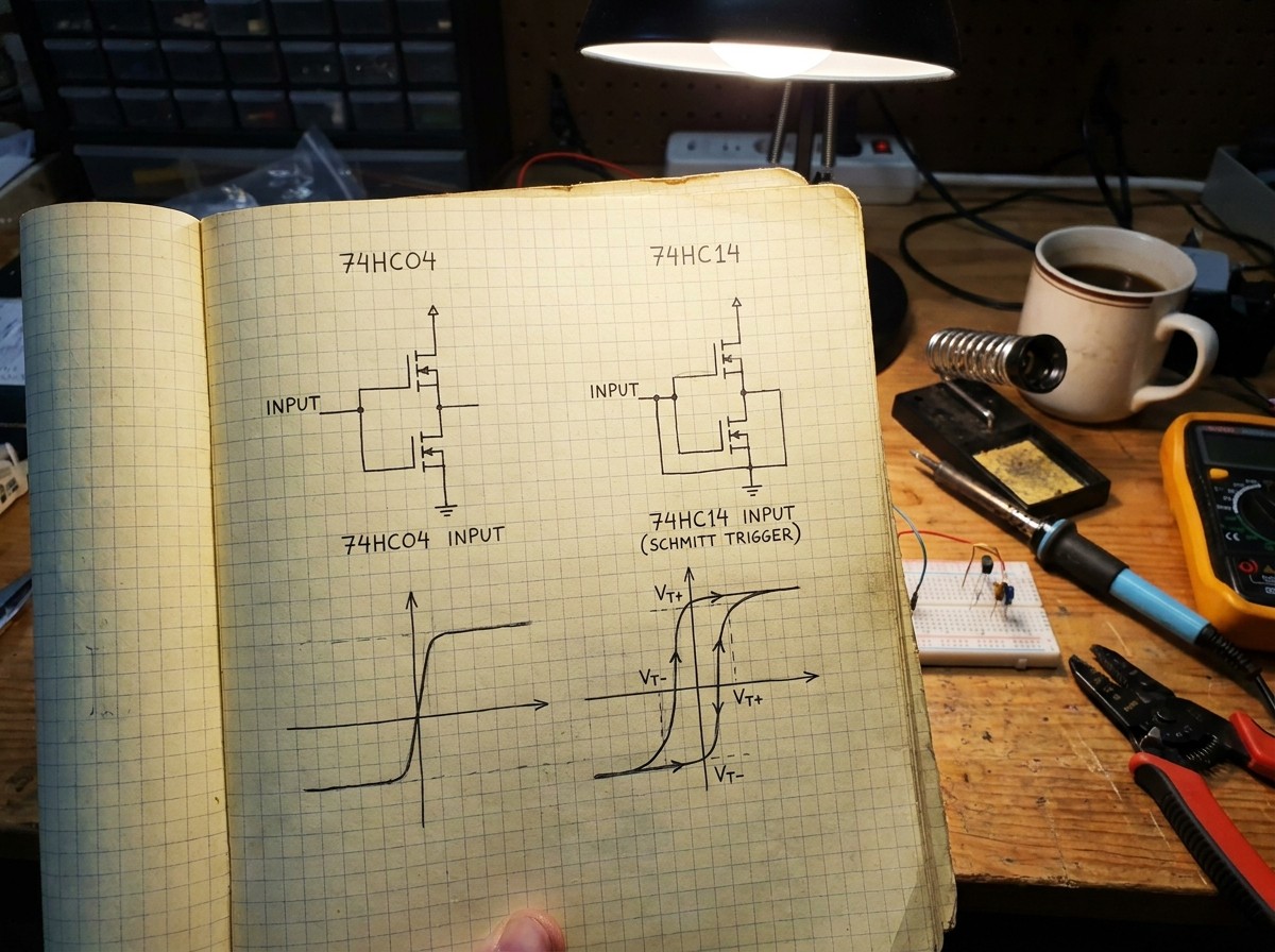
The 74HC04 Standard Input Stage
The 74HC04 input connects to a complementary pair of MOSFETs (a P-channel pull-up and an N-channel pull-down). This stage presents a single nominal switching threshold centered at roughly(guaranteed by standard JEDEC levels:minimum,maximum at). Because there is no internal feedback, any input voltage lingering betweenandplaces both MOSFETs into partial conduction.
The 74HC14 Schmitt-Trigger Input Stage
The 74HC14 incorporates internal positive feedback (cross-coupled source-follower structures) that alters the effective gate-source potential of the input transistors depending on the current output state:
When the input is rising from 0 V, the internal circuit holds the negative-side threshold down until the input reaches the positive-going threshold ().
When the input is falling from, the circuit holds the positive threshold high until the voltage drops to the negative-going threshold ().
The Hysteresis Band () acts as an integrated analog deadband. Voltage fluctuations, ripple, or high-frequency noise that remain smaller thancannot toggle the output state.
Parametric Electrical Comparison
Because threshold voltages vary across manufacturing processes, operating temperature (to/), and supply rail levels, designs must be verified against worst-case limits:
| Parameter | Test Condition () | 74HC04 (Standard) | 74HC14 (Schmitt-Trigger) | Unit |
|---|---|---|---|---|
| Positive-Going Threshold () | N/A () N/A () N/A () | 0.7 min / 1.2 typ / 1.5 max 1.55 min / 2.5 typ / 3.15 max[1] 2.1 min / 3.3 typ / 4.2 max | V | |
| Negative-Going Threshold () | N/A () N/A () N/A () | 0.3 min / 0.7 typ / 1.1 max 0.9 min / 1.6 typ / 2.45 max 1.2 min / 2.1 typ / 3.2 max | V | |
| Hysteresis Voltage ()** | None (nominal) None (nominal) None (nominal) | 0.2 min / 0.5 typ / 1.0 max 0.4 min / 0.9 typ / 2.1 max 0.5 min / 1.2 typ / 2.5 max | V | |
| Max Input Transition Time () | 1000 500 400 | No Limit () No Limit () No Limit () | ns | |
| Propagation Delay (, Typ / Max) | 9 / 19 | 12 / 25 | ns | |
| Quiescent Supply Current (, Max) | 20 | 20 |
The Dynamic Speed Penalty of Schmitt Inputs
The internal positive-feedback stages of the 74HC14 introduce a propagation delay penalty of approximatelycompared to the 74HC04 under identical load conditions (,). While negligible in human-interface and low-frequency sensor circuits, this delta creates timing skew when balancing parallel channels in nanosecond-scale synchronous buses.
3. The Physics of Slow-Edge Failure: Shoot-Through Current and Chattering
When a digital designer encounters unexplainable board resets, elevated current draw, or intermittent register clocking, the root cause is often a standard CMOS input driven by an insufficiently steep edge rate.
Linear Region Conduction and Shoot-Through (Crowbar Current)
In a CMOS push-pull gate, the upper P-channel MOSFET turns off when the input rises toward, while the lower N-channel MOSFET turns off when the input falls toward Ground. Under high-speed switching conditions (), the transition across the intermediate threshold is fast enough that both transistors are partially on for only picoseconds, resulting in negligible dynamic energy loss.
However, when an input signal moves slowly through the threshold region (), both the PMOS and NMOS gates enter their saturation/active regions simultaneously. This establishes a direct, low-impedance channel from the positive supply rail to Ground, known as shoot-through (crowbar) conduction.
How To Remove Stubborn IC 74HC04 74HC14 Hex Inverter And Schmitt Trigger Integrated Circuit
On a test bench, sweeping apotentiometer slowly across themidpoint of a 74HC04 powered by arail demonstrates this effect clearly:
As the wiper enters the switching region, output monitoring LEDs tied to both rails glow simultaneously because the output stage hovers at an indeterminate analog voltage.
The bench supply current monitor jumps from baseline microamps to 16–17 mA on a single gate.
In a 14-pin package where multiple gates are driven by slow signals, the combined shoot-through currents can exceed, causing measurable package heating, rail sag, and premature silicon degradation.
Repeating the identical test with a 74HC14 yields completely different behavior: the output snaps cleanly between logic states with zero simultaneous LED illumination, and supply current remains clamped at baseline quiescent levels throughout the sweep.
False Clocking and Output Chattering
Beyond excess power consumption, standard inverters driven by slow edges act as high-gain open-loop operational amplifiers. High-speed CMOS inverters possess small-signal voltage gains () exceedingin their linear regions.
If an analog ramp containing even microvolts of thermal noise, inductive ground bounce, or electromagnetic interference passes slowly through the narrow threshold of a 74HC04, that noise is amplified rail-to-rail. The output toggles high and low dozens of times during a single slow transition. If this output drives a hardware counter, an interrupt pin, or an SPI clock input, the receiving silicon registers multiple false triggers.
This behavior explains why Texas Instruments, Nexperia, and ON Semiconductor datasheets specify strict maximum input rise and fall time limits () for the 74HC04: capped atatandat. Violating this specification operates the device outside its certified electrical envelope. The 74HC14 carries no transition time limit (), making it immune to edge-rate-induced instability.
4. Circuit Application Boundaries and the Critical Oscillator Trap
Selecting between standard and Schmitt-trigger inverters is not simply a matter of picking the "cleaner" part; specific circuit topologies strictly require one architecture and fail with the other.
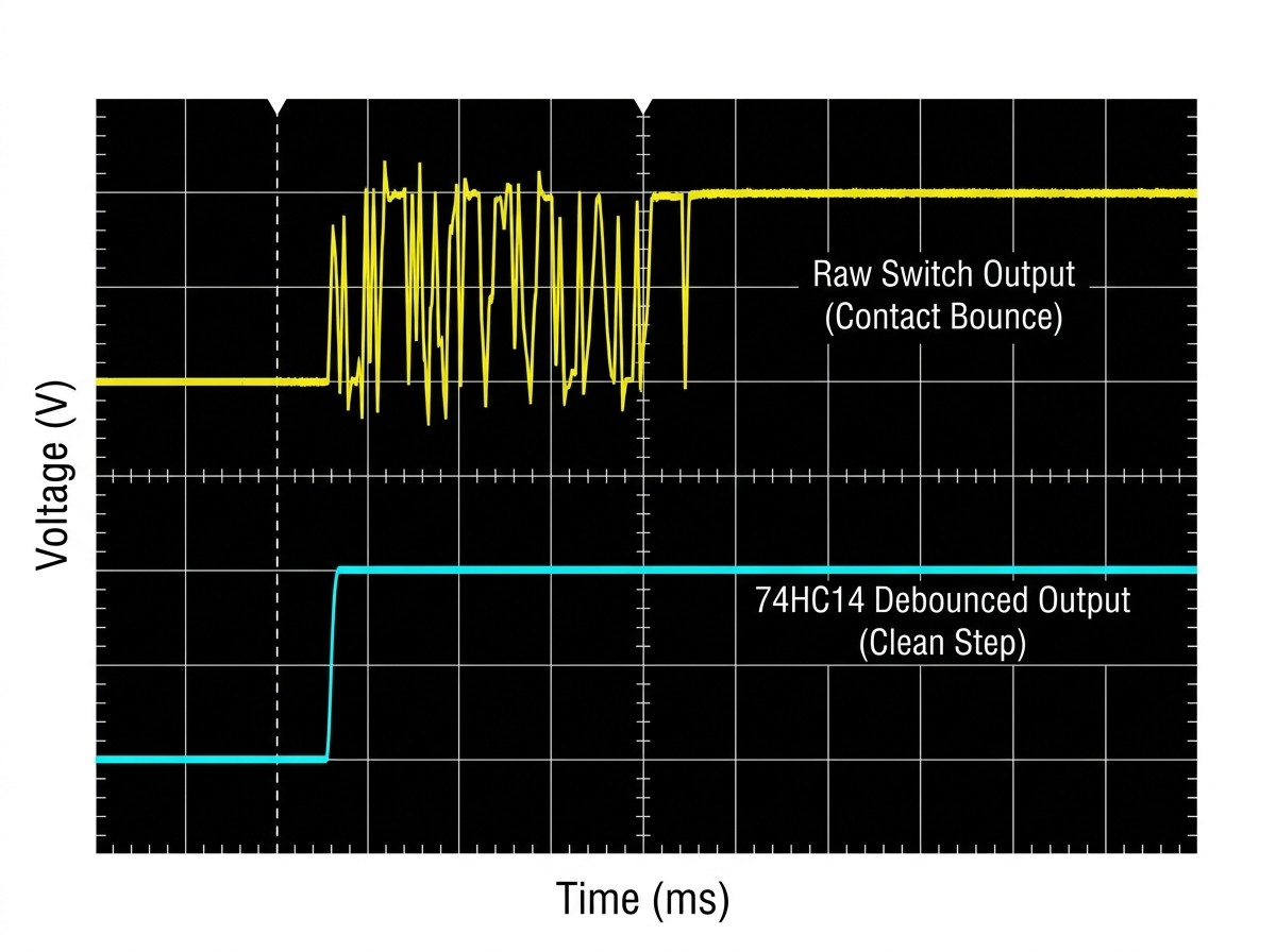
Case 1: Mechanical Switch Debouncing via Passive RC Filter
Mechanical switches and pushbuttons exhibit physical contact bounce, repeatedly making and breaking electrical contact forupon actuation. A simple hardware debouncer places a pull-up resistor, a series resistor, and a capacitor across the switch to form a low-pass filter.
The resulting waveform at the filter output is an exponential charging or discharging curve ().
Using a 74HC04: The exponential voltage spends hundreds of microseconds crossing the linear switching region (to). High-frequency noise superimposed on the capacitor voltage causes the standard gate to output a train of high-frequency noise bursts, failing to debounce the signal.
Using a 74HC14: The Schmitt trigger's positive-going threshold (at) and negative-going threshold () create a noise deadband (). Any bounce ripple smaller thanis ignored. The output transitions cleanly with a single, sharp edge.
Case 2: Simple RC Astable Relaxation Oscillators
A simple square-wave clock generator can be constructed using a single inverter, one resistor (), and one capacitor ().
Operation with 74HC14: When the output is HIGH, capacitorcharges throughtoward. Once the voltage reaches, the inverter output snaps LOW. The capacitor then discharges throughtowarduntil reaching, at which point the output snaps HIGH again. This cycle repeats continuously. The oscillation period () is defined by:
At, using nominal threshold ratios for high-speed CMOS, this simplifies to the standard rule-of-thumb:
Failure with 74HC04: Lacking hysteresis, a single 74HC04 inverter with negative feedback will not oscillate. Instead, negative feedback biases the gate into its linear region where. The gate stabilizes into a static DC equilibrium, producing zero clock output while drawing continuous shoot-through current.
Case 3: The Pierce Crystal Oscillator Pitfall
The most common mistake when substituting a 74HC14 into an existing board occurs in quartz crystal or ceramic resonator circuits.
A Pierce oscillator relies on a high-value feedback resistor (, typically) connected directly between the inverter’s output and input. The purpose ofis DC negative feedback, forcing the active element into the center of its linear transfer region where it operates as a high-gain inverting analog amplifier (). The quartz crystal, operating in its inductive region between series and parallel resonance, forms a pi-network with load capacitorsand, providing aphase shift. Combined with thephase inversion of the amplifier, this satisfies the Barkhausen criterion for sustained oscillation (loop gain, total phase shift).
Why the 74HC14 Fails: The internal positive feedback of the Schmitt trigger prevents the gate from operating as a linear analog amplifier. Whenfeeds output voltage back to the input, the gate cannot stabilize at an analog bias point; it snaps hard to eitheror. The input voltage cannot overcome the hysteresis threshold via the crystal, loop transconductance drops to zero, and the oscillator fails to start.
The Unbuffered Role (74HCU04): While a standard buffered 74HC04 can oscillate in basic crystal circuits, industry design rules recommend the unbuffered 74HCU04. A standard 74HC04 contains three cascaded internal inverter stages to provide high digital gain, which can introduce excess phase delay and parasitic high-frequency oscillation with AT-cut crystals. The 74HCU04 contains a single complementary MOSFET pair, providing a stable, linear transconductance amplifier without spurious overtone oscillation. Under no circumstances should a 74HC14 be used here.
Case 4: Long Cable Runs and Optocoupler Output Shaping
Phototransistors in optocouplers typically exhibit slow collector rise times () due to internal parasitic base-collector capacitance (Miller effect) when driven by weak pull-up resistors. Feeding an optocoupler collector directly into a standard 74HC04 violates thelimit, causing false triggers on the microcontroller bus. Placing a 74HC14 directly downstream squares up the slow edge into a sub-15 ns transition.
Similarly, signal lines traveling across ribbon cables or off-board wiring harnesses pick up magnetic cross-coupling and ground bounce. If a signal with ground bounce is processed by a 74HC04, any bounce exceeding the narrow single threshold triggers spurious logic levels. The 74HC14's wide hysteresis band filters out this common-mode noise.
5. Practical Bench Traps, Outdated Substitution Myths, and Sourcing Reality
Myth 1: "The 74HC14 is always a drop-in upgrade for the 74HC04"
Reality: Pin compatibility does not guarantee schematic compatibility. While a 74HC14 can safely replace a 74HC04 used purely for digital inversion or line buffering, substitution will disable crystal oscillators, analog integrators, and linear-biased operational filters.
Myth 2: "A Schmitt trigger can replace an analog comparator like an LM393"
Reality: Engineers sometimes attempt to save board space by using a spare 74HC14 gate as an analog voltage comparator. This approach is unreliable in production:
Standard analog comparators offer stable, differential inputs with millivolt-level offset voltages.
The 74HC14’s trip thresholds (and) carry broad process distributions (at,can range fromtoacross lots) and drift significantly with ambient temperature and supply voltage. The 74HC14 is a digital signal shaper, not an analog measurement device.
Myth 3: "74HC14 and 74HCT14 are completely interchangeable"
Reality: The "T" designation indicates TTL-compatible input thresholds.
The 74HC14 operates acrosstowith symmetric CMOS thresholds scaled to roughlyand.
The 74HCT14 is restricted to a narrowtosupply and features lower, asymmetric thresholds (typ,typ, guaranteed minimumat[2]) designed to interface with legacy 5 V TTL outputs (,). A 74HCT14 cannot be powered from arail, whereas a 74HC14 runs reliably at that voltage.
The Parasitic High-Frequency Burst Oscillation Trap
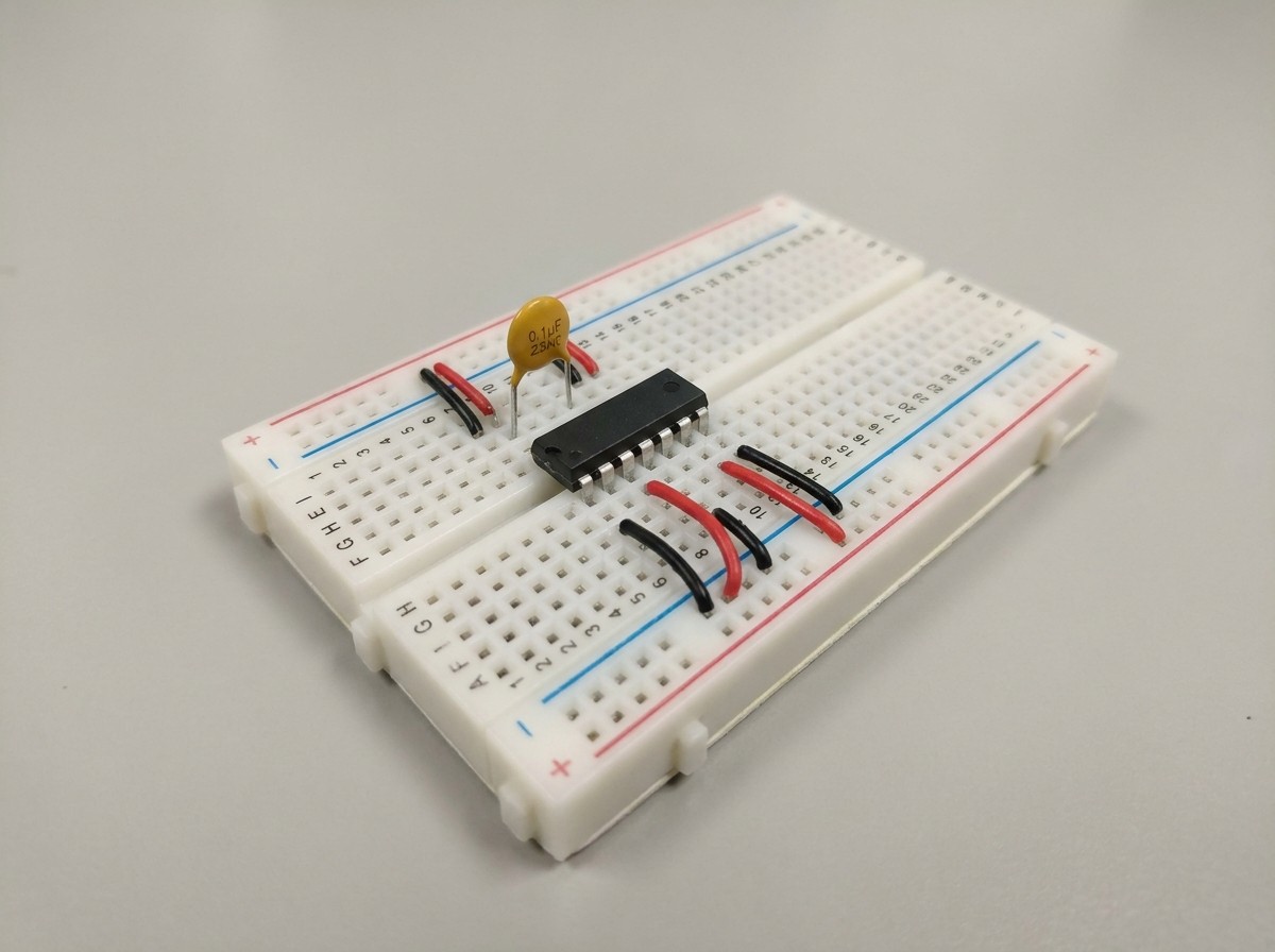
A documented edge-case occurs when feeding high-impedance () signals into a 74HC14 on an unbypassed breadboard or poorly routed PCB. When the input voltage passes through a trip point, the gate’s high internal gain-bandwidth product (internal silicon gain) can interact with package lead inductance and breadboard rail impedance, resulting in burst-oscillation at the threshold[6].
Without local power decoupling, this high-speed switching modulates the internal ground and supply rails, causing the input voltage relative to the die to bounce back across the trip threshold. The output can burst-oscillate at VHF frequencies () for several nanoseconds right at the trip point.
To prevent this:
Place alow-ESR ceramic capacitor (X7R) directly adjacent to Pin 14 (), routing with low inductance to Pin 7 (Ground).
Avoid driving Schmitt inputs with high-impedance sources without placing a small filter capacitor (e.g.,to) close to the input pin to provide a low-impedance AC path.
Bench Handling and Bring-Up Traps
The Reversed IC Gotcha: Accurately orient package notch indicators. Inserting a 14-pin DIP backward on a breadboard swaps Pin 14 () and Pin 7 (Ground). The internal ESD protection diodes between the substrate and power rails are placed across the supply in forward bias, shorting the rail.
Current-Limiting as a Guardrail: When powering a new logic breadboard for the first time, set the bench power supply current limit toat. If an IC is reversed, the supply will enter Constant Current (
CC) mode and clamp the rail below, saving the internal silicon from thermal destruction.The Floating Input Rule: Standard high-speed CMOS inputs have an input impedance of roughly. Leaving unused inverter inputs floating allows ambient electrostatic fields to bias the gates into the linear region, triggering internal shoot-through current and radiating switching noise to adjacent gates. Every unused input on both the 74HC04 and 74HC14 must be tied directly toor Ground.
6. Engineering Verification Checklist & Frequently Asked Questions
Engineering Pre-Flight Schematic Checklist
Signal Transition Rate (): Are all signals driving the 74HC04 verified to have transition times faster than(at)? If edges are slower or driven by passive RC circuits, has the component been changed to a 74HC14?
Oscillator Gate Selection: Are all quartz crystal or ceramic resonator circuits driven by unbuffered inverters (74HCU04) or standard inverters (74HC04)? Ensure no 74HC14 Schmitt trigger is placed in an analog feedback loop.
Supply Voltage Alignment: If using a 74HCT14, is the supply rail strictly withinto? If running fromto, is the 74HC14 selected instead?
Local Decoupling: Is aceramic bypass capacitor placed withinof Pin 14 with a direct, short return path to Pin 7?
Unused Gate Termination: Are the inputs of all unused inverter channels tied securely toor Ground? (Outputs must remain unconnected).
RC Oscillator Timing Tolerances: For 74HC14 relaxation oscillators, have frequency tolerances been modeled against worst-caseandspreads over temperature?
Frequently Asked Questions
Can a 74HC14 replace an analog comparator like an LM393?
No. An analog comparator like the LM393 provides a differential input stage, an adjustable reference threshold, low input offset voltage (typically), and predictable performance across temperature. The 74HC14 switches at single-ended, uncalibrated thresholds that vary from chip to chip and shift with temperature and supply rail fluctuations. Use the 74HC14 to condition degraded digital signals, not to measure analog voltages.
Can a 74HC14 replace a 555 timer?
For basic, non-critical square-wave clock generation, yes. A single 74HC14 inverter with one resistor and one capacitor forms a reliable astable multivibrator, saving PCB real estate and leaving five spare gates on the chip. However, a bipolar 555 timer provides high output drive current (up tosink/source compared tofor the 74HC14), independent charge/discharge duty-cycle control, and better frequency stability over supply voltage fluctuations.
What happens if an input to a 74HC14 floats?
Because CMOS inputs present near-infinite input impedance, an un-terminated pin accumulates electrostatic charge, floating into the intermediate voltage region. While the 74HC14's internal hysteresis prevents rapid chattering compared to a standard 74HC04, lingering near the switching threshold still turns on internal input transistors partially, increasing quiescent current draw () and coupling noise into adjacent gates on the die. All unused inputs must be tied toor Ground.
Why do crystal oscillator schematics specifically call for a 74HCU04 instead of a 74HC04 or 74HC14?
The "U" in 74HCU04 designates an unbuffered inverter consisting of a single complementary MOSFET pair. Standard buffered inverters (74HC04) contain three internal cascaded inverter stages to maximize digital output rise times. In a linear crystal oscillator feedback loop, these extra stages produce high voltage gain and parasitic phase shifts, making the circuit susceptible to high-frequency overtone oscillation or crystal overdrive. The 74HC14 cannot be used because its internal Schmitt hysteresis makes linear biasing acrossimpossible, preventing crystal resonance from starting.
Sources and references used for this guide
SNx4HC14 Hex Inverters with Schmitt-Trigger Inputs Datasheet
Source type: official company documentation
Used for: Authoritative electrical specifications, input threshold voltages (VT+, VT-), hysteresis band definitions, supply voltage range (2V to 6V), and drive ratings.74HC14; 74HCT14 Hex Inverting Schmitt Trigger Datasheet
Source type: official company documentation
Used for: Dynamic switching characteristics, propagation delay across temperature, transfer characteristic curves, and TTL-compatible 74HCT14 threshold comparisons.MC74HC14A Hex Schmitt-Trigger Inverter High-Performance Silicon-Gate CMOS Datasheet
Source type: official company documentation
Used for: Verification of pin-for-pin footprint compatibility with 74HC04/LS04, slow edge squaring application parameters, and package options.74HC04 Hex Inverter Pinout, Circuit and Datasheet
Source type: vendor article
Used for: Component pinout verification, standard inverter logic characteristics, internal gate layout, and circuit integration examples.74HC14 Schmitt Trigger Datasheet, Pinout and Application
Source type: vendor article
Used for: Schmitt-trigger application overviews, pin assignment confirmation, RC filter interfacing, and pulse-shaping circuits.Simplest 74HC14 + Potentiometer Circuit Fails with Self-Oscillation at Hysteresis Threshold
Source type: community discussion
Used for: Documenting real-world bench troubleshooting pitfalls, high-frequency parasitic burst oscillations, and bypassing requirements on slow/floating inputs.
Specifications
Parts with Similar Specs
- ImagePart NumberManufacturerPackage / CaseNumber of PinsLogic FunctionNumber of CircuitsPropagation DelaySupply VoltageQuiescent CurrentTechnologyView Compare
![74HC14S14-13]()
74HC14S14-13
14-SOIC (0.154, 3.90mm Width)
14
Inverter, Schmitt Trigger
6
190 ns
4.5 V
20 μA
CMOS
![74HC05D,112]()
14-SOIC (0.154, 3.90mm Width)
14
Buffer, Inverter
-
15 ns
5 V
2 μA
CMOS
![74HC04S14-13]()
14-SOIC (0.154, 3.90mm Width)
14
Inverter, Schmitt Trigger
6
15 ns
4.5 V
40 μA
CMOS


Datasheet PDF
- Environmental Information :
- RohsStatement :
- Datasheets :
 Texas Instruments MSP430F2122TRTV: A Technical Overview
29 February 2024164
 2SC4793 Transistor: 2SC4793, 2SC4793 Datasheet, Equivalent
18 December 202121858
 BB18 POWR-BAR Distribution: Datasheet, Features, Equivalents
12 January 20222042
 STM32F407VGT6 Microcontroller: 168MHz,100-LQFP, Pinout and Features
07 February 202214056
 PMV40UN2R Transistor: FET MOSFET, PMV40UN2R Datasheet, Pinout
04 March 20222204
 CC2530 Zigbee SoC Deep Dive: Datasheet, Pinout, and Modern Design Challenges
25 February 20261649
 onsemi BC846B Transistor Series Explained for Beginners
29 August 20251465
 STM32F405RGT6 MCU STMicroelectronics
30 April 202112193
 Why are TWS Earbuds so Popular?
17 July 20217463
 How to Find the Ideal Voltage Reference for Your Application
11 July 20251433
 How Do We Seize Investment Opportunities on the Eve of the Ultimate Human Energy Final?
12 July 20222347
 What is Instrument Transformer?
08 January 20227962
 Analysis of SiP (System in Package)
12 January 20229321
 A Complete Guide to Tantalum Capacitors in 2025
10 July 20254439
 RTD Sensors: Working Principle, Features and Applications
22 May 202513985
 SiC MOSFET Shortage 2026: Supply, Lead Times & Alternatives
02 July 20261836
Diodes Incorporated
In Stock
Minimum: 1 Multiples: 1
Qty
Unit Price
Ext Price
1
$0.292077
$0.29
10
$0.275544
$2.76
100
$0.259948
$25.99
500
$0.245234
$122.62
1000
$0.231352
$231.35
Not the price you want? Send RFQ Now and we'll contact you ASAP.
Inquire for More Quantity
![74LVC2G32HD4-7]() 74LVC2G32HD4-7
74LVC2G32HD4-7Diodes Incorporated
![74AUP2G06FW4-7]() 74AUP2G06FW4-7
74AUP2G06FW4-7Diodes Incorporated
![74LVC2G02HD4-7]() 74LVC2G02HD4-7
74LVC2G02HD4-7Diodes Incorporated
![74AHCT1G08W5-7]() 74AHCT1G08W5-7
74AHCT1G08W5-7Diodes Incorporated
![74AHC1G09W5-7]() 74AHC1G09W5-7
74AHC1G09W5-7Diodes Incorporated
![74LVC2G04W6-7]() 74LVC2G04W6-7
74LVC2G04W6-7Diodes Incorporated
![74LVC1G04SE-7]() 74LVC1G04SE-7
74LVC1G04SE-7Diodes Incorporated
![74AHC1G08SE-7]() 74AHC1G08SE-7
74AHC1G08SE-7Diodes Incorporated
![74LVC1G14SE-7]() 74LVC1G14SE-7
74LVC1G14SE-7Diodes Incorporated
![74LVC1G04W5-7]() 74LVC1G04W5-7
74LVC1G04W5-7Diodes Incorporated


