
 Product
 Brand
Brand Articles
 Tools
Tools
74HC14 Schmitt Trigger: Datasheet, Pinout and Application

13 ns ns 110 ns ns 8.7376mm mm Gates & Inverters 5.2mA mA 1.7526mm mm Surface Mount Surface Mount 2V~6V V 2μA μA


13 ns ns 110 ns ns 8.7376mm mm Gates & Inverters 5.2mA mA 1.7526mm mm Surface Mount Surface Mount 2V~6V V 2μA μA
74HC14 is a member of 74XXXX series ICs, which consists of LOGIC GATES. This article will unlock more details about 74HC14. There is a huge range of Semiconductors, Capacitors, Resistors and ICs in stock. Welcome RFQ.

Quick NOT gate 7414 74HC14 hex inverting schmitt trigger integrated circuit IC demonstration
74HC14 Pinout

74HC14 Pinout
| Pin Number | Description |
| INPUT OF INVERTING SCHMITT TRIGGER GATE | |
| 1 | 1A-INPUT of GATE 1 |
| 3 | 2A-INPUT of GATE 2 |
| 5 | 3A-INPUT of GATE 3 |
| 9 | 4A-INPUT of GATE 4 |
| 11 | 5A-INPUT of GATE 5 |
| 13 | 6A-INPUT of GATE 6 |
| SHARED TERMINALS | |
| 7 | GND- connected to ground |
| 14 | VCC-Connected to a positive voltage to provide power to all six gates |
| OUTPUT OF INVERTING SCHMITT TRIGGER GATE | |
| 2 | 1Y-OUTPUT of GATE 1 |
| 4 | 2Y-OUTPUT of GATE 2 |
| 6 | 3Y-OUTPUT of GATE 3 |
| 8 | 4Y-OUTPUT of GATE 4 |
| 10 | 5Y-OUTPUT of GATE 5 |
| 12 | 6Y-OUTPUT of GATE 6 |
74HC14 CAD Model
Symbol

74HC14 Symbol
Footprint

74HC14 Footprint
3D Model

74HC14 3D Model
74HC14 Description
The 74HC14 is identical in pinout to the LS14, LS04 and HC04. The device inputs are compatible with Standard CMOS outputs; with pullup resistors, they are compatible with LSTTL outputs. The HC14 is useful to “square up” slow input rise and fall times. Due to the hysteresis voltage of the Schmitt trigger, the HC14 finds applications in noisy environments.
Specifications
- TypeParameter
- Mount
In electronic components, the term "Mount" typically refers to the method or process of physically attaching or fixing a component onto a circuit board or other electronic device. This can involve soldering, adhesive bonding, or other techniques to secure the component in place. The mounting process is crucial for ensuring proper electrical connections and mechanical stability within the electronic system. Different components may have specific mounting requirements based on their size, shape, and function, and manufacturers provide guidelines for proper mounting procedures to ensure optimal performance and reliability of the electronic device.
Surface Mount - Mounting Type
The "Mounting Type" in electronic components refers to the method used to attach or connect a component to a circuit board or other substrate, such as through-hole, surface-mount, or panel mount.
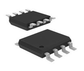
Surface Mount - Package / Case
refers to the protective housing that encases an electronic component, providing mechanical support, electrical connections, and thermal management.
14-SOIC (0.154, 3.90mm Width) - Number of Pins14
- Logic Level-High1.5V ~ 4.2V
- Logic Level-Low1V ~ 3V
- Operating Temperature
The operating temperature is the range of ambient temperature within which a power supply, or any other electrical equipment, operate in. This ranges from a minimum operating temperature, to a peak or maximum operating temperature, outside which, the power supply may fail.
-55°C~125°C - Packaging
Semiconductor package is a carrier / shell used to contain and cover one or more semiconductor components or integrated circuits. The material of the shell can be metal, plastic, glass or ceramic.
Tape & Reel (TR) - Series
In electronic components, the "Series" refers to a group of products that share similar characteristics, designs, or functionalities, often produced by the same manufacturer. These components within a series typically have common specifications but may vary in terms of voltage, power, or packaging to meet different application needs. The series name helps identify and differentiate between various product lines within a manufacturer's catalog.
74HC - Published2007
- JESD-609 Code
The "JESD-609 Code" in electronic components refers to a standardized marking code that indicates the lead-free solder composition and finish of electronic components for compliance with environmental regulations.
e3 - Pbfree Code
The "Pbfree Code" parameter in electronic components refers to the code or marking used to indicate that the component is lead-free. Lead (Pb) is a toxic substance that has been widely used in electronic components for many years, but due to environmental concerns, there has been a shift towards lead-free alternatives. The Pbfree Code helps manufacturers and users easily identify components that do not contain lead, ensuring compliance with regulations and promoting environmentally friendly practices. It is important to pay attention to the Pbfree Code when selecting electronic components to ensure they meet the necessary requirements for lead-free applications.
yes - Part Status
Parts can have many statuses as they progress through the configuration, analysis, review, and approval stages.
Obsolete - Moisture Sensitivity Level (MSL)
Moisture Sensitivity Level (MSL) is a standardized rating that indicates the susceptibility of electronic components, particularly semiconductors, to moisture-induced damage during storage and the soldering process, defining the allowable exposure time to ambient conditions before they require special handling or baking to prevent failures
1 (Unlimited) - Number of Terminations14
- Terminal Finish
Terminal Finish refers to the surface treatment applied to the terminals or leads of electronic components to enhance their performance and longevity. It can improve solderability, corrosion resistance, and overall reliability of the connection in electronic assemblies. Common finishes include nickel, gold, and tin, each possessing distinct properties suitable for various applications. The choice of terminal finish can significantly impact the durability and effectiveness of electronic devices.
Tin (Sn) - HTS Code
HTS (Harmonized Tariff Schedule) codes are product classification codes between 8-1 digits. The first six digits are an HS code, and the countries of import assign the subsequent digits to provide additional classification. U.S. HTS codes are 1 digits and are administered by the U.S. International Trade Commission.
8542.39.00.01 - Packing Method
The packing method in electronic components refers to the technique used to package and protect the component during shipping and handling. It encompasses various forms including tape and reel, tray, tube, or bulk packaging, each suited for different types of components and manufacturing processes. The choice of packing method can affect the ease of handling, storage, and the efficiency of assembly in automated processes. Additionally, it plays a crucial role in ensuring the reliability and integrity of the components until they are used in electronic devices.
TAPE AND REEL - Voltage - Supply
Voltage - Supply refers to the range of voltage levels that an electronic component or circuit is designed to operate with. It indicates the minimum and maximum supply voltage that can be applied for the device to function properly. Providing supply voltages outside this range can lead to malfunction, damage, or reduced performance. This parameter is critical for ensuring compatibility between different components in a circuit.
2V~6V - Terminal Position
In electronic components, the term "Terminal Position" refers to the physical location of the connection points on the component where external electrical connections can be made. These connection points, known as terminals, are typically used to attach wires, leads, or other components to the main body of the electronic component. The terminal position is important for ensuring proper connectivity and functionality of the component within a circuit. It is often specified in technical datasheets or component specifications to help designers and engineers understand how to properly integrate the component into their circuit designs.
DUAL - Terminal Form
Occurring at or forming the end of a series, succession, or the like; closing; concluding.
GULL WING - Peak Reflow Temperature (Cel)
Peak Reflow Temperature (Cel) is a parameter that specifies the maximum temperature at which an electronic component can be exposed during the reflow soldering process. Reflow soldering is a common method used to attach electronic components to a circuit board. The Peak Reflow Temperature is crucial because it ensures that the component is not damaged or degraded during the soldering process. Exceeding the specified Peak Reflow Temperature can lead to issues such as component failure, reduced performance, or even permanent damage to the component. It is important for manufacturers and assemblers to adhere to the recommended Peak Reflow Temperature to ensure the reliability and functionality of the electronic components.
260 - Number of Functions6
- Supply Voltage
Supply voltage refers to the electrical potential difference provided to an electronic component or circuit. It is crucial for the proper operation of devices, as it powers their functions and determines performance characteristics. The supply voltage must be within specified limits to ensure reliability and prevent damage to components. Different electronic devices have specific supply voltage requirements, which can vary widely depending on their design and intended application.
3V - Terminal Pitch
The center distance from one pole to the next.
1.27mm - Reach Compliance Code
Reach Compliance Code refers to a designation indicating that electronic components meet the requirements set by the Registration, Evaluation, Authorization, and Restriction of Chemicals (REACH) regulation in the European Union. It signifies that the manufacturer has assessed and managed the chemical substances within the components to ensure safety and environmental protection. This code is vital for compliance with regulations aimed at minimizing risks associated with hazardous substances in electronic products.
unknown - Time@Peak Reflow Temperature-Max (s)
Time@Peak Reflow Temperature-Max (s) refers to the maximum duration that an electronic component can be exposed to the peak reflow temperature during the soldering process, which is crucial for ensuring reliable solder joint formation without damaging the component.
40 - Base Part Number
The "Base Part Number" (BPN) in electronic components serves a similar purpose to the "Base Product Number." It refers to the primary identifier for a component that captures the essential characteristics shared by a group of similar components. The BPN provides a fundamental way to reference a family or series of components without specifying all the variations and specific details.
74HC14 - Pin Count
a count of all of the component leads (or pins)
14 - Qualification Status
An indicator of formal certification of qualifications.
Not Qualified - Operating Supply Voltage
The voltage level by which an electrical system is designated and to which certain operating characteristics of the system are related.
5V - Supply Voltage-Max (Vsup)
The parameter "Supply Voltage-Max (Vsup)" in electronic components refers to the maximum voltage that can be safely applied to the component without causing damage. It is an important specification to consider when designing or using electronic circuits to ensure the component operates within its safe operating limits. Exceeding the maximum supply voltage can lead to overheating, component failure, or even permanent damage. It is crucial to adhere to the specified maximum supply voltage to ensure the reliable and safe operation of the electronic component.
6V - Supply Voltage-Min (Vsup)
The parameter "Supply Voltage-Min (Vsup)" in electronic components refers to the minimum voltage level required for the component to operate within its specified performance range. This parameter indicates the lowest voltage that can be safely applied to the component without risking damage or malfunction. It is crucial to ensure that the supply voltage provided to the component meets or exceeds this minimum value to ensure proper functionality and reliability. Failure to adhere to the specified minimum supply voltage may result in erratic behavior, reduced performance, or even permanent damage to the component.
2V - Number of Circuits6
- Load Capacitance
the amount of capacitance measured or computed across the crystal terminals on the PCB. Frequency Tolerance. Frequency tolerance refers to the allowable deviation from nominal, in parts per million (PPM), at a specific temperature, usually +25°C.
50pF - Output Current
The rated output current is the maximum load current that a power supply can provide at a specified ambient temperature. A power supply can never provide more current that it's rated output current unless there is a fault, such as short circuit at the load.
5.2mA - Propagation Delay
the flight time of packets over the transmission link and is limited by the speed of light.
13 ns - Quiescent Current
The quiescent current is defined as the current level in the amplifier when it is producing an output of zero.
2μA - Turn On Delay Time
Turn-on delay, td(on), is the time taken to charge the input capacitance of the device before drain current conduction can start.
110 ns - Family
In electronic components, the parameter "Family" typically refers to a categorization or classification system used to group similar components together based on their characteristics, functions, or applications. This classification helps users easily identify and select components that meet their specific requirements. The "Family" parameter can include various subcategories such as resistors, capacitors, diodes, transistors, integrated circuits, and more. Understanding the "Family" of an electronic component can provide valuable information about its compatibility, performance specifications, and potential uses within a circuit or system. It is important to consider the "Family" parameter when designing or troubleshooting electronic circuits to ensure proper functionality and compatibility with other components.
HC/UH - Logic Function
In electronic components, the term "Logic Function" refers to the specific operation or behavior of a component based on its input signals. It describes how the component processes the input signals to produce the desired output. Logic functions are fundamental to digital circuits and are used to perform logical operations such as AND, OR, NOT, and XOR.Each electronic component, such as logic gates or flip-flops, is designed to perform a specific logic function based on its internal circuitry. By understanding the logic function of a component, engineers can design and analyze complex digital systems to ensure proper functionality and performance. Different logic functions can be combined to create more complex operations, allowing for the creation of sophisticated digital devices and systems.
Buffer, Inverter - Logic Type
Logic Type in electronic components refers to the classification of circuits based on the logical operations they perform. It includes types such as AND, OR, NOT, NAND, NOR, XOR, and XNOR, each defining the relationship between binary inputs and outputs. The logic type determines how the inputs affect the output state based on specific rules of Boolean algebra. This classification is crucial for designing digital circuits and systems, enabling engineers to select appropriate components for desired functionalities.
Inverter - Max I(ol)
Max I(ol) refers to the maximum output current that a specific electronic component, such as a transistor or integrated circuit, can sink or source. This parameter is crucial in determining the capability of the component to drive external loads without being damaged. It is typically specified in the component's datasheet and is important for ensuring proper operation and reliability of the circuit in which the component is used. Designers must ensure that the output current requirements of the circuit do not exceed the specified "Max I(ol)" value to prevent overloading and potential failure of the component.
0.004 A - Max Propagation Delay @ V, Max CL
The parameter "Max Propagation Delay @ V, Max CL" in electronic components refers to the maximum amount of time it takes for a signal to propagate through the component from input to output when operating at a specific voltage (V) and driving a maximum specified load capacitance (CL). This parameter is crucial in determining the speed and performance of the component in a circuit. A shorter propagation delay indicates faster signal processing and better overall performance. Designers use this parameter to ensure that signals can be transmitted and received within the required timing constraints in their electronic systems.
13ns @ 6V, 50pF - Prop. Delay@Nom-Sup
The parameter "Prop. Delay@Nom-Sup" in electronic components refers to the propagation delay at nominal supply voltage. Propagation delay is the time it takes for a signal to travel from the input of a component to the output, typically measured in nanoseconds or picoseconds. The nominal supply voltage is the standard operating voltage specified for the component.This parameter is important because it affects the overall speed and performance of the electronic circuit. A shorter propagation delay means faster signal processing and better overall performance. Designers need to consider the propagation delay at the nominal supply voltage when selecting components for their circuits to ensure proper functionality and meet performance requirements.
22 ns - Schmitt Trigger
A Schmitt Trigger is a type of comparator circuit commonly used in electronics to convert an analog input signal into a digital output signal. It has hysteresis, which means that the output switches at different voltage levels depending on whether the input is rising or falling. This hysteresis helps to eliminate noise and provide a more stable output signal. Schmitt Triggers are often used in applications where noise immunity and signal conditioning are important, such as in signal processing, waveform shaping, and digital logic circuits.
YES - Features
In the context of electronic components, the term "Features" typically refers to the specific characteristics or functionalities that a particular component offers. These features can vary depending on the type of component and its intended use. For example, a microcontroller may have features such as built-in memory, analog-to-digital converters, and communication interfaces like UART or SPI.When evaluating electronic components, understanding their features is crucial in determining whether they meet the requirements of a particular project or application. Engineers and designers often look at features such as operating voltage, speed, power consumption, and communication protocols to ensure compatibility and optimal performance.In summary, the "Features" parameter in electronic components describes the unique attributes and capabilities that differentiate one component from another, helping users make informed decisions when selecting components for their electronic designs.
Schmitt Trigger - Height1.7526mm
- Length8.7376mm
- Width3.9878mm
- RoHS Status
RoHS means “Restriction of Certain Hazardous Substances” in the “Hazardous Substances Directive” in electrical and electronic equipment.
RoHS Compliant - Lead Free
Lead Free is a term used to describe electronic components that do not contain lead as part of their composition. Lead is a toxic material that can have harmful effects on human health and the environment, so the electronics industry has been moving towards lead-free components to reduce these risks. Lead-free components are typically made using alternative materials such as silver, copper, and tin. Manufacturers must comply with regulations such as the Restriction of Hazardous Substances (RoHS) directive to ensure that their products are lead-free and environmentally friendly.
Lead Free
74HC14 Feature
•Output Drive Capability: 10 LSTTL Loads
• Outputs Directly Interface to CMOS, NMOS and TTL
• Operating Voltage Range: 2.0 to 6.0 V
• Low Input Current: 1.0 A
• High Noise Immunity Characteristic of CMOS Devices
• In Compliance With the JEDEC Standard No. 7A Requirements
• ESD Performance: HBM 2000 V; Machine Model 200 V
• Chip Complexity: 60 FETs or 15 Equivalent Gates
• These are Pb−Free Devices
74HC14 Application
General-purpose logic
PCs and notebooks
TV, DVD, Set-Top Box
Networking
Digital systems
74HC14 Equivalent
The equivalent parts for 74HC14:
MC14584
CD40106
Where to use 74HC14
Consider the following scenarios to better understand how 74HC14 is used:
Case 1: You need to convert signal waveforms to square waveforms. Non-square waveforms can be converted to square waves using Schmitt trigger gates on the 74HC14. We can convert sinusoidal or triangular waves to square waves using the Schmitt trigger gate.
Case 2: When a logic inverter is required. This chip's inverter Schmitt triggers can generate output that is negated logic input. Inverted logics for controllers or digital electronics can be obtained using these chip gates.
When you wish to get rid of noise in digital electronics, use Case3. In digital circuits, noise creates significant errors, hence the 74HC14 chip is excellent.
How to use 74HC14
As previously stated, the 74HC14 includes six INVERTING SCHMITT TRIGGER GATES that can be used individually. The logic diagram can be summarized as follows.

74HC14 Logic Diagram
Now, to better understand how gates work, let's take a single gate and attach the power to the chip. Also, at the input, provide an analogue signal.

74HC14 Circuit
As shown in the circuit, we are giving a sinusoidal wave at the input and taking Vout as the output of the gate. Once we draw the input and output graph we will have something like this.

74HC14 Trigger Application
The Schmitt Trigger operates on a very basic principle: the output of an inverting Schmitt Trigger is LOW only when the input signal voltage level crosses the threshold voltage (+Vt).
As illustrated in the diagram, the output voltage (Vout) is HIGH until the input voltage (Vin) surpasses the threshold voltage (Vt+). The output voltage becomes LOW once it hits the threshold voltage. Until the input voltage falls below the low threshold voltage, the output voltage remains low (Vt-). The output voltage hits HIGH once it reaches that point. This cycle continues.
As illustrated in the graph, when a sinusoidal signal is used as an input, the result is a square wave. Each gate can be used in this manner to obtain the required output.
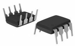
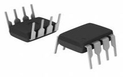
74HC14 Package


74HC14 Package
74HC14 Manufacturer
On Semiconductor (Nasdaq: ON) is a manufacturer engaging itself in reducing energy use. It features a comprehensive portfolio of power, signal management, and logic, custom solutions that are energy efficient. It acts as a world-class supply chain with high reliability and a network of manufacturing facilities, sales, offices, and design centers in key markets through North America, Europe, and the Asia Pacific regions.
Parts with Similar Specs
- ImagePart NumberManufacturerPackage / CaseNumber of PinsLogic FunctionNumber of CircuitsPropagation DelaySupply VoltageQuiescent CurrentTechnologyView Compare
![74HC14DR2G]()
74HC14DR2G
14-SOIC (0.154, 3.90mm Width)
14
Buffer, Inverter
6
13 ns
3 V
2 μA
CMOS
![SN74HC04D]()
14-SOIC (0.154, 3.90mm Width)
14
Buffer, Inverter
6
13 ns
3 V
2 μA
CMOS
![74HCU04DR2G]()
14-SOIC (0.154, 3.90mm Width)
14
-
-
16 ns
5 V
2 μA
CMOS
![74HC04DR2G]()
14-SOIC (0.154, 3.90mm Width)
14
-
-
16 ns
5 V
2 μA
CMOS
![SN74HC04DR]()
14-SOIC (0.154, 3.90mm Width)
14
-
6
12 ns
3 V
2 μA
CMOS


Datasheet PDF
- Datasheets :
- ReachStatement :
- PCN Obsolescence/ EOL :
Popularity by Region
How do I use a 74HC14 as an oscillator?
When a capacitor and resistor are added to a Schmitt Trigger gate, as shown in the first circuit of Fig: 5 above, the result is an oscillator called a MULTIVIBRATOR. A multivibrator has the feature of producing a square wave and this waveshape can have equal high and low periods (called 50:50 mark:space ratio) or any ratio of high and low periods. The HIGH period is called the MARK and the LOW is called the SPACE.
Where can I find various 74HC14 VCO circuits?
This is a Simple VCO circuit using Schmitt trigger as Figure 1 is a Voltage-controlled Oscillator (VCO) by use the 74HC14 IC, which inside the IC include up to 6 Schmitt trigger, but applied just only one can also be the frequency controller by voltage.
How do I hookup the 74HC14 to Arduino?
Here are the signals you get when the button is pressed (top) or released (bottom). Yellow is the output of the RC filter and red is the (digital) output of the Schmitt-triggered buffer. Note that the 74HC14 is an inverting buffer so the output signal goes from low to high when the button is pressed.
 LME49720 Audio Operational Amplifier: Circuit, Price and Alternatives
29 June 20215588
 LT3045:High Performance Regulator
22 March 20225590
 1N5062 Diode: Features, Pinout, and Datasheet
18 January 20222405
 DS1307N Real-Time Clock: Circuit, Pinout, and Datasheet
17 April 20251355
 DS1990A iButton: Where & How to use
03 November 20214200
 AD8479 Precision Difference Amplifier: Pinout and Basic Connections
12 November 20211887
 Unveiling the Microchip PIC24HJ32GP302/304 Microcontroller Series: A Technical Deep Dive
29 February 2024200
 A Comprehensive Guide to LTC6907HS6#TRMPBF Programmable Timer and Oscillator
06 March 2024287
 How to Distinguish MOSFET? Is it N-Channel or P-Channel?
23 December 202111265
 Solenoid Switch: Working Principle, Types and Applications
03 February 202127432
 What are Resonators?
07 January 202617631
 The Underappreciated iphone - No One Believed Apple CEO Steve Jobs Would Succeed Before
01 July 20224654
 What is Amplifier?
08 November 20257939
 Emerging Trends in Complex Programmable Logic Devices Market 2025
16 June 2025907
 Will HBM replace DDR and become Computer Memory?
09 September 202126742
 Reed Relays: 10 Key Applications in Modern Electronics
04 July 20253047
ON Semiconductor
In Stock: 37500
United States
China
Canada
Japan
Russia
Germany
United Kingdom
Singapore
Italy
Hong Kong(China)
Taiwan(China)
France
Korea
Mexico
Netherlands
Malaysia
Austria
Spain
Switzerland
Poland
Thailand
Vietnam
India
United Arab Emirates
Afghanistan
Åland Islands
Albania
Algeria
American Samoa
Andorra
Angola
Anguilla
Antigua & Barbuda
Argentina
Armenia
Aruba
Australia
Azerbaijan
Bahamas
Bahrain
Bangladesh
Barbados
Belarus
Belgium
Belize
Benin
Bermuda
Bhutan
Bolivia
Bonaire, Sint Eustatius and Saba
Bosnia & Herzegovina
Botswana
Brazil
British Indian Ocean Territory
British Virgin Islands
Brunei
Bulgaria
Burkina Faso
Burundi
Cabo Verde
Cambodia
Cameroon
Cayman Islands
Central African Republic
Chad
Chile
Christmas Island
Cocos (Keeling) Islands
Colombia
Comoros
Congo
Congo (DRC)
Cook Islands
Costa Rica
Côte d’Ivoire
Croatia
Cuba
Curaçao
Cyprus
Czechia
Denmark
Djibouti
Dominica
Dominican Republic
Ecuador
Egypt
El Salvador
Equatorial Guinea
Eritrea
Estonia
Eswatini
Ethiopia
Falkland Islands
Faroe Islands
Fiji
Finland
French Guiana
French Polynesia
Gabon
Gambia
Georgia
Ghana
Gibraltar
Greece
Greenland
Grenada
Guadeloupe
Guam
Guatemala
Guernsey
Guinea
Guinea-Bissau
Guyana
Haiti
Honduras
Hungary
Iceland
Indonesia
Iran
Iraq
Ireland
Isle of Man
Israel
Jamaica
Jersey
Jordan
Kazakhstan
Kenya
Kiribati
Kosovo
Kuwait
Kyrgyzstan
Laos
Latvia
Lebanon
Lesotho
Liberia
Libya
Liechtenstein
Lithuania
Luxembourg
Macao(China)
Madagascar
Malawi
Maldives
Mali
Malta
Marshall Islands
Martinique
Mauritania
Mauritius
Mayotte
Micronesia
Moldova
Monaco
Mongolia
Montenegro
Montserrat
Morocco
Mozambique
Myanmar
Namibia
Nauru
Nepal
New Caledonia
New Zealand
Nicaragua
Niger
Nigeria
Niue
Norfolk Island
North Korea
North Macedonia
Northern Mariana Islands
Norway
Oman
Pakistan
Palau
Palestinian Authority
Panama
Papua New Guinea
Paraguay
Peru
Philippines
Pitcairn Islands
Portugal
Puerto Rico
Qatar
Réunion
Romania
Rwanda
Samoa
San Marino
São Tomé & Príncipe
Saudi Arabia
Senegal
Serbia
Seychelles
Sierra Leone
Sint Maarten
Slovakia
Slovenia
Solomon Islands
Somalia
South Africa
South Sudan
Sri Lanka
St Helena, Ascension, Tristan da Cunha
St. Barthélemy
St. Kitts & Nevis
St. Lucia
St. Martin
St. Pierre & Miquelon
St. Vincent & Grenadines
Sudan
Suriname
Svalbard & Jan Mayen
Sweden
Syria
Tajikistan
Tanzania
Timor-Leste
Togo
Tokelau
Tonga
Trinidad & Tobago
Tunisia
Turkey
Turkmenistan
Turks & Caicos Islands
Tuvalu
U.S. Outlying Islands
U.S. Virgin Islands
Uganda
Ukraine
Uruguay
Uzbekistan
Vanuatu
Vatican City
Venezuela
Wallis & Futuna
Yemen
Zambia
Zimbabwe
![MC74LCX08DTR2G]() MC74LCX08DTR2G
MC74LCX08DTR2GON Semiconductor
![MC74HC1G08DTT1G]() MC74HC1G08DTT1G
MC74HC1G08DTT1GON Semiconductor
![MC14011BDR2G]() MC14011BDR2G
MC14011BDR2GON Semiconductor
![NC7SZ04P5X]() NC7SZ04P5X
NC7SZ04P5XON Semiconductor
![MC74HC04ADR2G]() MC74HC04ADR2G
MC74HC04ADR2GON Semiconductor
![NC7SZ04M5X]() NC7SZ04M5X
NC7SZ04M5XON Semiconductor
![NC7WZ14P6X]() NC7WZ14P6X
NC7WZ14P6XON Semiconductor
![NC7WZ04P6X]() NC7WZ04P6X
NC7WZ04P6XON Semiconductor
![MM74HC14MX]() MM74HC14MX
MM74HC14MXON Semiconductor
![74VHC14MTCX]() 74VHC14MTCX
74VHC14MTCXON Semiconductor


