
 Product
 Brand
Brand Articles
 Tools
Tools
TPS22965 Load Switch: Datasheet, Pinout, Typical Application Circuit


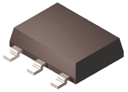
N-Channel 0.5mm Gold PMIC TPS22965 8 Pin 5V 8-WFDFN Exposed Pad
The TPS22965 is a single channel load switch. This article mainly covers its pinout, datasheet, typical application circuit and more about TPS22965.
TPS22965 Pinout

TPS22965 Pinout
TPS22965 CAD Model
Symbol

TPS22965 Symbol
Footprint

TPS22965 Footprint
3D Model

TPS22965 3D Model
TPS22965 Overview
The TPS22965 is a single channel load switch that provides configurable rise time to minimize inrush current. The device contains an N-channel MOSFET that can operate over an input voltage range of 0.8 V to 5.7 V and can support a maximum continuous current of 6 A. The switch is controlled by an on/off input (ON), which is capable of interfacing directly with low-voltage control signals. In the TPS22965, a 225-0 on-chip load resistor is added for quick output discharge when the switch is turned off The TPS22965 is available in a small, space-saving 2.00 mm x 2.00 mm 8-pin SON package (DSG) with an integrated thermal pad allowing for high power dissipation. The device is characterized for operation over the free-air temperature range of - -40 °C to 105 °C.
TPS22965 Feature
Integrated Single Channel Load Switch
Input Voltage Range: 0.7 V to 5 .7 V
RON Resistance
RON = 14 mΩ at VIN = 5 V (VBIAS = 5 V)
5-A Maximum Continuous Switch Current
Adjustable Undervoltage Lockout Threshold (UVLO)
Adjustable Voltage Supervisor with Power Good (PG) Indicator
Adjustable Output Slew Rate Control
Enhanced Quick Output Discharge Remains Active after Power is Removed (TPS22954 Only)
15 Ω (Typ) Discharges 100 µF Within 10 ms
Reverse Current Blocking when Disabled (TPS22953 Only)
Automatic Restart after Supervisor Fault Detection When Enabled
Thermal Shutdown
Low Quiescent Current ≤ 50 µA
SON 10 -pin Package with Thermal Pad
ESD Performance Tested Per JESD 22
2-kV HBM and 750 -V CDM
TPS22965 Application
●UltrabookTM
●Notebooks/Netbooks
●Tablet PC
●Consumer Electronics
●Set-top Boxes/Residential Gateways
●Telecom Systems
●Solid State Drives (SSDs)
TPS22965 Functional Block Diagram
The TPS22965 device is a single channel, 6-A load switch in an 8-pin SON package. To reduce the voltage drop in high current rails, the device implements an ultra-low resistance N-channel MOSFET. The device has a programmable slew rate for applications that require specific rise-time. The device has a very low leakage current during off state. This prevents downstream circuits from pulling high standby current from the supply. Integrated control logic, driver, power supply, and output discharge FETeliminates the need for any external components, which reduces solution size and bill of materials (BOM) count. The functional block diagram is shown below.

TPS22965 Functional Block Diagram
TPS22965 Typical Application Circuit
This application demonstrates how the TPS22965 can be used to power downstream modules.

TPS22965-Powering a Downstream Module
TPS22965 Package

TPS22965 Package
Specifications
- TypeParameter
- Lifecycle Status
Lifecycle Status refers to the current stage of an electronic component in its product life cycle, indicating whether it is active, obsolete, or transitioning between these states. An active status means the component is in production and available for purchase. An obsolete status indicates that the component is no longer being manufactured or supported, and manufacturers typically provide a limited time frame for support. Understanding the lifecycle status is crucial for design engineers to ensure continuity and reliability in their projects.
ACTIVE (Last Updated: 5 days ago) - Factory Lead Time6 Weeks
- Contact Plating
Contact plating (finish) provides corrosion protection for base metals and optimizes the mechanical and electrical properties of the contact interfaces.
Gold - Mount
In electronic components, the term "Mount" typically refers to the method or process of physically attaching or fixing a component onto a circuit board or other electronic device. This can involve soldering, adhesive bonding, or other techniques to secure the component in place. The mounting process is crucial for ensuring proper electrical connections and mechanical stability within the electronic system. Different components may have specific mounting requirements based on their size, shape, and function, and manufacturers provide guidelines for proper mounting procedures to ensure optimal performance and reliability of the electronic device.
Surface Mount - Mounting Type
The "Mounting Type" in electronic components refers to the method used to attach or connect a component to a circuit board or other substrate, such as through-hole, surface-mount, or panel mount.
Surface Mount - Package / Case
refers to the protective housing that encases an electronic component, providing mechanical support, electrical connections, and thermal management.
8-WFDFN Exposed Pad - Number of Pins8
- Turn Off Delay Time
It is the time from when Vgs drops below 90% of the gate drive voltage to when the drain current drops below 90% of the load current. It is the delay before current starts to transition in the load, and depends on Rg. Ciss.
80 μs - Operating Temperature
The operating temperature is the range of ambient temperature within which a power supply, or any other electrical equipment, operate in. This ranges from a minimum operating temperature, to a peak or maximum operating temperature, outside which, the power supply may fail.
-40°C~105°C TA - Packaging
Semiconductor package is a carrier / shell used to contain and cover one or more semiconductor components or integrated circuits. The material of the shell can be metal, plastic, glass or ceramic.
Tape & Reel (TR) - JESD-609 Code
The "JESD-609 Code" in electronic components refers to a standardized marking code that indicates the lead-free solder composition and finish of electronic components for compliance with environmental regulations.
e4 - Pbfree Code
The "Pbfree Code" parameter in electronic components refers to the code or marking used to indicate that the component is lead-free. Lead (Pb) is a toxic substance that has been widely used in electronic components for many years, but due to environmental concerns, there has been a shift towards lead-free alternatives. The Pbfree Code helps manufacturers and users easily identify components that do not contain lead, ensuring compliance with regulations and promoting environmentally friendly practices. It is important to pay attention to the Pbfree Code when selecting electronic components to ensure they meet the necessary requirements for lead-free applications.
yes - Part Status
Parts can have many statuses as they progress through the configuration, analysis, review, and approval stages.
Active - Moisture Sensitivity Level (MSL)
Moisture Sensitivity Level (MSL) is a standardized rating that indicates the susceptibility of electronic components, particularly semiconductors, to moisture-induced damage during storage and the soldering process, defining the allowable exposure time to ambient conditions before they require special handling or baking to prevent failures
2 (1 Year) - Number of Terminations8
- ECCN Code
An ECCN (Export Control Classification Number) is an alphanumeric code used by the U.S. Bureau of Industry and Security to identify and categorize electronic components and other dual-use items that may require an export license based on their technical characteristics and potential for military use.
EAR99 - Resistance
Resistance is a fundamental property of electronic components that measures their opposition to the flow of electric current. It is denoted by the symbol "R" and is measured in ohms (Ω). Resistance is caused by the collisions of electrons with atoms in a material, which generates heat and reduces the flow of current. Components with higher resistance will impede the flow of current more than those with lower resistance. Resistance plays a crucial role in determining the behavior and functionality of electronic circuits, such as limiting current flow, voltage division, and controlling power dissipation.
25mOhm - Terminal Position
In electronic components, the term "Terminal Position" refers to the physical location of the connection points on the component where external electrical connections can be made. These connection points, known as terminals, are typically used to attach wires, leads, or other components to the main body of the electronic component. The terminal position is important for ensuring proper connectivity and functionality of the component within a circuit. It is often specified in technical datasheets or component specifications to help designers and engineers understand how to properly integrate the component into their circuit designs.
DUAL - Peak Reflow Temperature (Cel)
Peak Reflow Temperature (Cel) is a parameter that specifies the maximum temperature at which an electronic component can be exposed during the reflow soldering process. Reflow soldering is a common method used to attach electronic components to a circuit board. The Peak Reflow Temperature is crucial because it ensures that the component is not damaged or degraded during the soldering process. Exceeding the specified Peak Reflow Temperature can lead to issues such as component failure, reduced performance, or even permanent damage to the component. It is important for manufacturers and assemblers to adhere to the recommended Peak Reflow Temperature to ensure the reliability and functionality of the electronic components.
260 - Number of Functions1
- Supply Voltage
Supply voltage refers to the electrical potential difference provided to an electronic component or circuit. It is crucial for the proper operation of devices, as it powers their functions and determines performance characteristics. The supply voltage must be within specified limits to ensure reliability and prevent damage to components. Different electronic devices have specific supply voltage requirements, which can vary widely depending on their design and intended application.
5V - Terminal Pitch
The center distance from one pole to the next.
0.5mm - Base Part Number
The "Base Part Number" (BPN) in electronic components serves a similar purpose to the "Base Product Number." It refers to the primary identifier for a component that captures the essential characteristics shared by a group of similar components. The BPN provides a fundamental way to reference a family or series of components without specifying all the variations and specific details.
TPS22965 - Number of Outputs1
- Output Type
The "Output Type" parameter in electronic components refers to the type of signal or data that is produced by the component as an output. This parameter specifies the nature of the output signal, such as analog or digital, and can also include details about the voltage levels, current levels, frequency, and other characteristics of the output signal. Understanding the output type of a component is crucial for ensuring compatibility with other components in a circuit or system, as well as for determining how the output signal can be utilized or processed further. In summary, the output type parameter provides essential information about the nature of the signal that is generated by the electronic component as its output.
N-Channel - Max Output Current
The maximum current that can be supplied to the load.
6A - Supply Voltage-Min (Vsup)
The parameter "Supply Voltage-Min (Vsup)" in electronic components refers to the minimum voltage level required for the component to operate within its specified performance range. This parameter indicates the lowest voltage that can be safely applied to the component without risking damage or malfunction. It is crucial to ensure that the supply voltage provided to the component meets or exceeds this minimum value to ensure proper functionality and reliability. Failure to adhere to the specified minimum supply voltage may result in erratic behavior, reduced performance, or even permanent damage to the component.
2.5V - Interface
In electronic components, the term "Interface" refers to the point at which two different systems, devices, or components connect and interact with each other. It can involve physical connections such as ports, connectors, or cables, as well as communication protocols and standards that facilitate the exchange of data or signals between the connected entities. The interface serves as a bridge that enables seamless communication and interoperability between different parts of a system or between different systems altogether. Designing a reliable and efficient interface is crucial in ensuring proper functionality and performance of electronic components and systems.
On/Off - Output Configuration
Output Configuration in electronic components refers to the arrangement or setup of the output pins or terminals of a device. It defines how the output signals are structured and how they interact with external circuits or devices. The output configuration can determine the functionality and compatibility of the component in a circuit design. Common types of output configurations include single-ended, differential, open-drain, and push-pull configurations, each serving different purposes and applications in electronic systems. Understanding the output configuration of a component is crucial for proper integration and operation within a circuit.
High Side - Output Current
The rated output current is the maximum load current that a power supply can provide at a specified ambient temperature. A power supply can never provide more current that it's rated output current unless there is a fault, such as short circuit at the load.
6A - Voltage - Supply (Vcc/Vdd)
Voltage - Supply (Vcc/Vdd) is a key parameter in electronic components that specifies the voltage level required for the proper operation of the device. It represents the power supply voltage that needs to be provided to the component for it to function correctly. This parameter is crucial as supplying the component with the correct voltage ensures that it operates within its specified limits and performance characteristics. It is typically expressed in volts (V) and is an essential consideration when designing and using electronic circuits to prevent damage and ensure reliable operation.
0.8V~5.7V - Quiescent Current
The quiescent current is defined as the current level in the amplifier when it is producing an output of zero.
50μA - Input Type
Input type in electronic components refers to the classification of the signal or data that a component can accept for processing or conversion. It indicates whether the input is analog, digital, or a specific format such as TTL or CMOS. Understanding input type is crucial for ensuring compatibility between different electronic devices and circuits, as it determines how signals are interpreted and interacted with.
Non-Inverting - Turn On Delay Time
Turn-on delay, td(on), is the time taken to charge the input capacitance of the device before drain current conduction can start.
2.2 ms - Switch Type
Based on their characteristics, there are basically three types of switches: Linear switches, tactile switches and clicky switches.
General Purpose - Nominal Input Voltage
The actual voltage at which a circuit operates can vary from the nominal voltage within a range that permits satisfactory operation of equipment. The word “nominal” means “named”.
5.7V - Output Polarity
Output polarity in electronic components refers to the orientation of the output signal in relation to the ground or reference voltage. It indicates whether the output voltage is positive or negative with respect to the ground. Positive output polarity means the signal is higher than the ground potential, while negative output polarity signifies that the signal is lower than the ground. This characteristic is crucial for determining compatibility with other components in a circuit and ensuring proper signal processing.
TRUE - Ratio - Input:Output
The parameter "Ratio - Input:Output" in electronic components refers to the relationship between the input and output quantities of a device or system. It is a measure of how the input signal or energy is transformed or converted into the output signal or energy. This ratio is often expressed as a numerical value or percentage, indicating the efficiency or effectiveness of the component in converting the input to the desired output. A higher ratio typically signifies better performance or higher efficiency, while a lower ratio may indicate losses or inefficiencies in the conversion process. Understanding and optimizing the input-output ratio is crucial in designing and evaluating electronic components for various applications.
1:1 - Input Characteristics
In electronic components, "Input Characteristics" refer to the set of specifications that describe how the component behaves in response to signals or inputs applied to it. These characteristics typically include parameters such as input voltage, input current, input impedance, input capacitance, and input frequency range. Understanding the input characteristics of a component is crucial for designing circuits and systems, as it helps ensure compatibility and proper functioning. By analyzing these parameters, engineers can determine how the component will interact with the signals it receives and make informed decisions about its use in a particular application.
STANDARD - Voltage - Load
Voltage - Load refers to the voltage across a load component in an electronic circuit when it is connected and operational. It represents the electrical potential difference that drives current through the load, which can be a resistor, motor, or other devices that consume electrical power. The voltage - load relationship is crucial for determining how much power the load will utilize and how it will affect the overall circuit performance. Properly managing voltage - load is essential for ensuring devices operate efficiently and safely within their specified limits.
2.5V~5.7V - Driver Number of Bits1
- Rds On (Typ)
The parameter "Rds On (Typ)" in electronic components refers to the typical on-state resistance of a MOSFET (Metal-Oxide-Semiconductor Field-Effect Transistor) when it is fully conducting. This parameter indicates the resistance encountered by the current flowing through the MOSFET when it is in the on-state, which affects the power dissipation and efficiency of the component. A lower Rds On value indicates better conduction and lower power loss in the MOSFET. Designers often consider this parameter when selecting components for applications where minimizing power loss and maximizing efficiency are critical factors.
16m Ω - Max Junction Temperature (Tj)
Max Junction Temperature (Tj) refers to the maximum allowable temperature at the junction of a semiconductor device, such as a transistor or integrated circuit. It is a critical parameter that influences the performance, reliability, and lifespan of the component. Exceeding this temperature can lead to thermal runaway, breakdown, or permanent damage to the device. Proper thermal management is essential to ensure the junction temperature remains within safe operating limits during device operation.
125°C - Built-in Protections
Built-in protections in electronic components refer to the safety features and mechanisms that are integrated into the component to prevent damage or malfunction in various situations. These protections are designed to safeguard the component from overvoltage, overcurrent, overheating, short circuits, and other potential hazards that could occur during operation. By having built-in protections, electronic components can operate more reliably and safely, extending their lifespan and reducing the risk of failure. These protections are essential for ensuring the overall performance and longevity of electronic devices and systems.
TRANSIENT - Features
In the context of electronic components, the term "Features" typically refers to the specific characteristics or functionalities that a particular component offers. These features can vary depending on the type of component and its intended use. For example, a microcontroller may have features such as built-in memory, analog-to-digital converters, and communication interfaces like UART or SPI.When evaluating electronic components, understanding their features is crucial in determining whether they meet the requirements of a particular project or application. Engineers and designers often look at features such as operating voltage, speed, power consumption, and communication protocols to ensure compatibility and optimal performance.In summary, the "Features" parameter in electronic components describes the unique attributes and capabilities that differentiate one component from another, helping users make informed decisions when selecting components for their electronic designs.
Load Discharge, Slew Rate Controlled - On-State Resistance
On-State Resistance, often denoted as Rds(on), refers to the resistance offered by a semiconductor device, such as a MOSFET or a diode, when it is in the "on" state and conducting current. This parameter is critical in determining the efficiency of the component, as lower on-state resistance results in reduced power loss and heat generation during operation. It is typically measured in ohms and can vary based on the specific device characteristics, current level, and temperature.
25mOhm - Height800μm
- Length2mm
- Width2mm
- Thickness
Thickness in electronic components refers to the measurement of how thick a particular material or layer is within the component structure. It can pertain to various aspects, such as the thickness of a substrate, a dielectric layer, or conductive traces. This parameter is crucial as it impacts the electrical, mechanical, and thermal properties of the component, influencing its performance and reliability in electronic circuits.
750μm - REACH SVHC
The parameter "REACH SVHC" in electronic components refers to the compliance with the Registration, Evaluation, Authorization, and Restriction of Chemicals (REACH) regulation regarding Substances of Very High Concern (SVHC). SVHCs are substances that may have serious effects on human health or the environment, and their use is regulated under REACH to ensure their safe handling and minimize their impact.Manufacturers of electronic components need to declare if their products contain any SVHCs above a certain threshold concentration and provide information on the safe use of these substances. This information allows customers to make informed decisions about the potential risks associated with using the components and take appropriate measures to mitigate any hazards.Ensuring compliance with REACH SVHC requirements is essential for electronics manufacturers to meet regulatory standards, protect human health and the environment, and maintain transparency in their supply chain. It also demonstrates a commitment to sustainability and responsible manufacturing practices in the electronics industry.
No SVHC - Radiation Hardening
Radiation hardening is the process of making electronic components and circuits resistant to damage or malfunction caused by high levels of ionizing radiation, especially for environments in outer space (especially beyond the low Earth orbit), around nuclear reactors and particle accelerators, or during nuclear accidents or nuclear warfare.
No - RoHS Status
RoHS means “Restriction of Certain Hazardous Substances” in the “Hazardous Substances Directive” in electrical and electronic equipment.
ROHS3 Compliant - Lead Free
Lead Free is a term used to describe electronic components that do not contain lead as part of their composition. Lead is a toxic material that can have harmful effects on human health and the environment, so the electronics industry has been moving towards lead-free components to reduce these risks. Lead-free components are typically made using alternative materials such as silver, copper, and tin. Manufacturers must comply with regulations such as the Restriction of Hazardous Substances (RoHS) directive to ensure that their products are lead-free and environmentally friendly.
Lead Free
Parts with Similar Specs
- ImagePart NumberManufacturerPackage / CaseNumber of PinsNumber of OutputsMax Output CurrentOutput CurrentInterfaceSupply VoltageNumber of TerminationsView Compare
![TPS22965DSGR]()
TPS22965DSGR
8-WFDFN Exposed Pad
8
1
6 A
6 A
On/Off
5 V
8
![TPS22967DSGR]()
8-TSSOP, 8-MSOP (0.118, 3.00mm Width) Exposed Pad
8
1
2 A
2 A
On/Off
5 V
8
![AP2141SG-13]()
8-SOIC (0.154, 3.90mm Width)
8
1
500 mA
-
On/Off
5 V
8
![AP2401MP-13]()
8-SOIC (0.154, 3.90mm Width)
8
1
2 A
2 A
On/Off
5 V
8
![AP2411S-13]()
8-WFDFN Exposed Pad
8
1
4 A
4 A
On/Off
5 V
8


What is the TPS22965?
Single-channel load switch
What type of MOSFET does the TPS22965 contain?
N-channel MOSFET.
What temperature range is the TPS22965 characterized for operation over?
105 °C.
What does the TPS22965 implement to reduce the voltage drop in high current rails?
Ultra-low resistance.
What does the TPS22965 device have for applications that require specific rise-time?
Programmable slew rate
 Leading Substitutes for onsemi BCP56 Transistor in 2025
19 August 2025258
 NE5532 - Dual Low Noise Op-Amp
09 December 20219313
 TL071CD Operational Amplifier: Pinout, Specification, and Datasheet
16 August 20242938
 Microchip PIC24FJ64GA004IPT: Technical Overview
29 February 2024223
 CD4050 hex buffer:Pinout, Alternatives, Datasheet PDF
02 July 20214651
 PCM5100APWR Audio Stereo DAC: Diagram, Pinout, and Datasheet
11 April 20221223
 AD936x Series RF Agile Transceiver: Wideband Performance Review and SDR Design Guide
10 February 2026281
![CDSOT23-SM712 Tvs Diode Surface SOT-23-3 14V Clamp[FAQ]: Datasheet, Pinout, and Applications](https://res.utmel.com/Images/Article/9fea5c62-7b3d-490f-89eb-f71899f86d2b.png) CDSOT23-SM712 Tvs Diode Surface SOT-23-3 14V Clamp[FAQ]: Datasheet, Pinout, and Applications
CDSOT23-SM712 Tvs Diode Surface SOT-23-3 14V Clamp[FAQ]: Datasheet, Pinout, and Applications02 April 20222291
 What is a Digital Potentiometer?
08 January 20267495
 Radiation Robustness of Gallium Nitride Power Devices
16 January 20242458
 Addressing Vulnerabilities in the U.S. Semiconductor Market
27 October 20231854
 RF Modulator: Working Principle and Development Trend
21 April 20217877
 Challenges and Issues in Smart Grid Infrastructure
11 May 20234065
 Introduction to MSP430 Microcontroller
26 December 202511153
 Introduction to PCB Layout Principles
13 November 20206405
 Review of IoT-Based Smart Home Security Systems- Part 1
28 March 20243646
Texas Instruments
In Stock: 30000
United States
China
Canada
Japan
Russia
Germany
United Kingdom
Singapore
Italy
Hong Kong(China)
Taiwan(China)
France
Korea
Mexico
Netherlands
Malaysia
Austria
Spain
Switzerland
Poland
Thailand
Vietnam
India
United Arab Emirates
Afghanistan
Åland Islands
Albania
Algeria
American Samoa
Andorra
Angola
Anguilla
Antigua & Barbuda
Argentina
Armenia
Aruba
Australia
Azerbaijan
Bahamas
Bahrain
Bangladesh
Barbados
Belarus
Belgium
Belize
Benin
Bermuda
Bhutan
Bolivia
Bonaire, Sint Eustatius and Saba
Bosnia & Herzegovina
Botswana
Brazil
British Indian Ocean Territory
British Virgin Islands
Brunei
Bulgaria
Burkina Faso
Burundi
Cabo Verde
Cambodia
Cameroon
Cayman Islands
Central African Republic
Chad
Chile
Christmas Island
Cocos (Keeling) Islands
Colombia
Comoros
Congo
Congo (DRC)
Cook Islands
Costa Rica
Côte d’Ivoire
Croatia
Cuba
Curaçao
Cyprus
Czechia
Denmark
Djibouti
Dominica
Dominican Republic
Ecuador
Egypt
El Salvador
Equatorial Guinea
Eritrea
Estonia
Eswatini
Ethiopia
Falkland Islands
Faroe Islands
Fiji
Finland
French Guiana
French Polynesia
Gabon
Gambia
Georgia
Ghana
Gibraltar
Greece
Greenland
Grenada
Guadeloupe
Guam
Guatemala
Guernsey
Guinea
Guinea-Bissau
Guyana
Haiti
Honduras
Hungary
Iceland
Indonesia
Iran
Iraq
Ireland
Isle of Man
Israel
Jamaica
Jersey
Jordan
Kazakhstan
Kenya
Kiribati
Kosovo
Kuwait
Kyrgyzstan
Laos
Latvia
Lebanon
Lesotho
Liberia
Libya
Liechtenstein
Lithuania
Luxembourg
Macao(China)
Madagascar
Malawi
Maldives
Mali
Malta
Marshall Islands
Martinique
Mauritania
Mauritius
Mayotte
Micronesia
Moldova
Monaco
Mongolia
Montenegro
Montserrat
Morocco
Mozambique
Myanmar
Namibia
Nauru
Nepal
New Caledonia
New Zealand
Nicaragua
Niger
Nigeria
Niue
Norfolk Island
North Korea
North Macedonia
Northern Mariana Islands
Norway
Oman
Pakistan
Palau
Palestinian Authority
Panama
Papua New Guinea
Paraguay
Peru
Philippines
Pitcairn Islands
Portugal
Puerto Rico
Qatar
Réunion
Romania
Rwanda
Samoa
San Marino
São Tomé & Príncipe
Saudi Arabia
Senegal
Serbia
Seychelles
Sierra Leone
Sint Maarten
Slovakia
Slovenia
Solomon Islands
Somalia
South Africa
South Sudan
Sri Lanka
St Helena, Ascension, Tristan da Cunha
St. Barthélemy
St. Kitts & Nevis
St. Lucia
St. Martin
St. Pierre & Miquelon
St. Vincent & Grenadines
Sudan
Suriname
Svalbard & Jan Mayen
Sweden
Syria
Tajikistan
Tanzania
Timor-Leste
Togo
Tokelau
Tonga
Trinidad & Tobago
Tunisia
Turkey
Turkmenistan
Turks & Caicos Islands
Tuvalu
U.S. Outlying Islands
U.S. Virgin Islands
Uganda
Ukraine
Uruguay
Uzbekistan
Vanuatu
Vatican City
Venezuela
Wallis & Futuna
Yemen
Zambia
Zimbabwe
![TPS22913CYZVR]() TPS22913CYZVR
TPS22913CYZVRTexas Instruments
![TPS2052BDR]() TPS2052BDR
TPS2052BDRTexas Instruments
![TPS2051BDGNR]() TPS2051BDGNR
TPS2051BDGNRTexas Instruments
![TPS2044BD]() TPS2044BD
TPS2044BDTexas Instruments
![TPS2042BDR]() TPS2042BDR
TPS2042BDRTexas Instruments
![ULQ2003ADR]() ULQ2003ADR
ULQ2003ADRTexas Instruments
![TPS22945DCKR]() TPS22945DCKR
TPS22945DCKRTexas Instruments
![TPS2042BDGN]() TPS2042BDGN
TPS2042BDGNTexas Instruments
![TPS2557DRBT]() TPS2557DRBT
TPS2557DRBTTexas Instruments
![TPS2044BDR]() TPS2044BDR
TPS2044BDRTexas Instruments


