
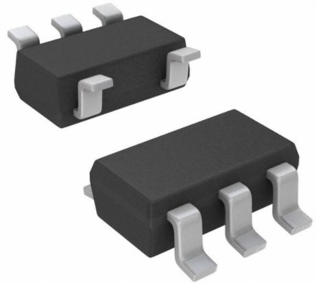
NE5532 - Dual Low Noise Op-Amp

38mA per Channel 200nA 70 dB Instrumentational OP Amps 1μA ±3V~20V NE5532 8 Pins 8-SOIC (0.154, 3.90mm Width)


38mA per Channel 200nA 70 dB Instrumentational OP Amps 1μA ±3V~20V NE5532 8 Pins 8-SOIC (0.154, 3.90mm Width)
The NE5532 is a Dual Low Noise Op-Amp in 8-pin package commonly used as amplifiers in audio circuits for its noise immunity and high output drive capability. The Op-Amp is internally compensated for high unity gain with maximum output swing bandwidth, low distortion and high slew rate. Furthermore, Huge range of Semiconductors, Capacitors, Resistors and IcS in stock. Welcome RFQ.

Operational amplifier step response test NE5532, TL072, LM833, LM4562
NE5532 Pinout

Pinout

NE5532 Pinout
| Pin Number | Pin Name | Description |
| 1 | OUTPUTA | Output of Op-Amp A |
| 2 | INPUTA- | Inverting Input of Op-Amp A |
| 3 | INPUTA+ | Non-Inverting Input of Op-Amp A |
| 4 | VEE,GND | Ground or Negative Supply Voltage |
| 5 | INPUTB+ | Non-Inverting Input of Op-Amp B |
| 6 | INPUTB- | Inverting Input of Op-Amp B |
| 7 | OUTPUTB | Output of Op-Amp B |
| 8 | VCC | Positive Supply Voltage |
NE5532 CAD Model

PCB Symbol

PCB Footprint

3D Model
NE5532 Description
The NE5532 is a dual high-performance low noise operational amplifier. Compared to most of the standard operational amplifiers, such as the 1458, it shows better noise performance, improved output drive capability and considerably higher small-signal and power bandwidths. This makes the device especially suitable for application in high-quality and professional audio equipment, instrumentation and control circuits, and telephone channel amplifiers. The op amp is internally compensated for gains equal to one. If very low noise is of prime importance, it is recommended that the 5532A version be used because it has guaranteed noise voltage specifications.
The NE5532 is a Low Noise Audio amplifier IC. The IC features a very low noise with unity gain internal compensation. The gain of the IC is upto to 5000 and hence is commonly used in audio pre-amplifier circuits. Since the IC is highly immune to noise it is commonly preferred in sensitive audio signal conditioning designs. The Op-Amp also has a low range operating voltage from ±3V to ±20V and hence can be used in wide variety of voltage ranges. The Op-Amp can also has wide bandwidth and slew rate and hence can be used in frequency selection, enabling you control bass or treble of a audio signals and play it in different modes like Rock, Jazz etc.
This article provides you with a basic overview of the NE5532 Dual Low Noise Op-Amp, including its pin descriptions, features and specifications, etc., to help you quickly understand what NE5532 is.
NE5532 Features
● Small-Signal Bandwidth: 10 MHz
● Output Drive Capability: 600 Ω, 10 VRMS
● Input Noise Voltage: 5.0 nV/√Hz (Typical)
● DC Voltage Gain: 50000
● AC Voltage Gain: 2200 at 10 kHz
● Power Bandwidth: 140 kHz
● Slew Rate: 9.0 V/μs
● Large Supply Voltage Range: ±3.0 to ±20 V
● Compensated for Unity Gain
● Pb−Free Packages are Available
Specifications
- TypeParameter
- Lifecycle Status
Lifecycle Status refers to the current stage of an electronic component in its product life cycle, indicating whether it is active, obsolete, or transitioning between these states. An active status means the component is in production and available for purchase. An obsolete status indicates that the component is no longer being manufactured or supported, and manufacturers typically provide a limited time frame for support. Understanding the lifecycle status is crucial for design engineers to ensure continuity and reliability in their projects.
ACTIVE (Last Updated: 4 days ago) - Factory Lead Time4 Weeks
- Contact Plating
Contact plating (finish) provides corrosion protection for base metals and optimizes the mechanical and electrical properties of the contact interfaces.
Tin - Mounting Type
The "Mounting Type" in electronic components refers to the method used to attach or connect a component to a circuit board or other substrate, such as through-hole, surface-mount, or panel mount.
Surface Mount - Package / Case
refers to the protective housing that encases an electronic component, providing mechanical support, electrical connections, and thermal management.
8-SOIC (0.154, 3.90mm Width) - Surface Mount
having leads that are designed to be soldered on the side of a circuit board that the body of the component is mounted on.
YES - Number of Pins8
- Number of Elements2
- Operating Temperature
The operating temperature is the range of ambient temperature within which a power supply, or any other electrical equipment, operate in. This ranges from a minimum operating temperature, to a peak or maximum operating temperature, outside which, the power supply may fail.
0°C~70°C - Packaging
Semiconductor package is a carrier / shell used to contain and cover one or more semiconductor components or integrated circuits. The material of the shell can be metal, plastic, glass or ceramic.
Tube - Published2002
- JESD-609 Code
The "JESD-609 Code" in electronic components refers to a standardized marking code that indicates the lead-free solder composition and finish of electronic components for compliance with environmental regulations.
e3 - Pbfree Code
The "Pbfree Code" parameter in electronic components refers to the code or marking used to indicate that the component is lead-free. Lead (Pb) is a toxic substance that has been widely used in electronic components for many years, but due to environmental concerns, there has been a shift towards lead-free alternatives. The Pbfree Code helps manufacturers and users easily identify components that do not contain lead, ensuring compliance with regulations and promoting environmentally friendly practices. It is important to pay attention to the Pbfree Code when selecting electronic components to ensure they meet the necessary requirements for lead-free applications.
yes - Part Status
Parts can have many statuses as they progress through the configuration, analysis, review, and approval stages.
Active - Moisture Sensitivity Level (MSL)
Moisture Sensitivity Level (MSL) is a standardized rating that indicates the susceptibility of electronic components, particularly semiconductors, to moisture-induced damage during storage and the soldering process, defining the allowable exposure time to ambient conditions before they require special handling or baking to prevent failures
1 (Unlimited) - Number of Terminations8
- ECCN Code
An ECCN (Export Control Classification Number) is an alphanumeric code used by the U.S. Bureau of Industry and Security to identify and categorize electronic components and other dual-use items that may require an export license based on their technical characteristics and potential for military use.
EAR99 - Packing Method
The packing method in electronic components refers to the technique used to package and protect the component during shipping and handling. It encompasses various forms including tape and reel, tray, tube, or bulk packaging, each suited for different types of components and manufacturing processes. The choice of packing method can affect the ease of handling, storage, and the efficiency of assembly in automated processes. Additionally, it plays a crucial role in ensuring the reliability and integrity of the components until they are used in electronic devices.
RAIL - Max Power Dissipation
The maximum power that the MOSFET can dissipate continuously under the specified thermal conditions.
780mW - Terminal Position
In electronic components, the term "Terminal Position" refers to the physical location of the connection points on the component where external electrical connections can be made. These connection points, known as terminals, are typically used to attach wires, leads, or other components to the main body of the electronic component. The terminal position is important for ensuring proper connectivity and functionality of the component within a circuit. It is often specified in technical datasheets or component specifications to help designers and engineers understand how to properly integrate the component into their circuit designs.
DUAL - Terminal Form
Occurring at or forming the end of a series, succession, or the like; closing; concluding.
GULL WING - Peak Reflow Temperature (Cel)
Peak Reflow Temperature (Cel) is a parameter that specifies the maximum temperature at which an electronic component can be exposed during the reflow soldering process. Reflow soldering is a common method used to attach electronic components to a circuit board. The Peak Reflow Temperature is crucial because it ensures that the component is not damaged or degraded during the soldering process. Exceeding the specified Peak Reflow Temperature can lead to issues such as component failure, reduced performance, or even permanent damage to the component. It is important for manufacturers and assemblers to adhere to the recommended Peak Reflow Temperature to ensure the reliability and functionality of the electronic components.
260 - Number of Functions2
- Supply Voltage
Supply voltage refers to the electrical potential difference provided to an electronic component or circuit. It is crucial for the proper operation of devices, as it powers their functions and determines performance characteristics. The supply voltage must be within specified limits to ensure reliability and prevent damage to components. Different electronic devices have specific supply voltage requirements, which can vary widely depending on their design and intended application.
15V - Time@Peak Reflow Temperature-Max (s)
Time@Peak Reflow Temperature-Max (s) refers to the maximum duration that an electronic component can be exposed to the peak reflow temperature during the soldering process, which is crucial for ensuring reliable solder joint formation without damaging the component.
40 - Base Part Number
The "Base Part Number" (BPN) in electronic components serves a similar purpose to the "Base Product Number." It refers to the primary identifier for a component that captures the essential characteristics shared by a group of similar components. The BPN provides a fundamental way to reference a family or series of components without specifying all the variations and specific details.
NE5532 - Pin Count
a count of all of the component leads (or pins)
8 - Power Supplies
an electronic circuit that converts the voltage of an alternating current (AC) into a direct current (DC) voltage.?
+-15V - Operating Supply Current
Operating Supply Current, also known as supply current or quiescent current, is a crucial parameter in electronic components that indicates the amount of current required for the device to operate under normal conditions. It represents the current drawn by the component from the power supply while it is functioning. This parameter is important for determining the power consumption of the component and is typically specified in datasheets to help designers calculate the overall power requirements of their circuits. Understanding the operating supply current is essential for ensuring proper functionality and efficiency of electronic systems.
8mA - Nominal Supply Current
Nominal current is the same as the rated current. It is the current drawn by the motor while delivering rated mechanical output at its shaft.
8mA - Power Dissipation
the process by which an electronic or electrical device produces heat (energy loss or waste) as an undesirable derivative of its primary action.
780mW - Output Current
The rated output current is the maximum load current that a power supply can provide at a specified ambient temperature. A power supply can never provide more current that it's rated output current unless there is a fault, such as short circuit at the load.
38mA - Slew Rate
the maximum rate of output voltage change per unit time.
9V/μs - Architecture
In electronic components, the parameter "Architecture" refers to the overall design and structure of the component. It encompasses the arrangement of internal components, the layout of circuitry, and the physical form of the component. The architecture of an electronic component plays a crucial role in determining its functionality, performance, and compatibility with other components in a system. Different architectures can result in variations in power consumption, speed, size, and other key characteristics of the component. Designers often consider the architecture of electronic components carefully to ensure optimal performance and integration within a larger system.
VOLTAGE-FEEDBACK - Amplifier Type
Amplifier Type refers to the classification or categorization of amplifiers based on their design, functionality, and characteristics. Amplifiers are electronic devices that increase the amplitude of a signal, such as voltage or current. The type of amplifier determines its specific application, performance capabilities, and operating characteristics. Common types of amplifiers include operational amplifiers (op-amps), power amplifiers, audio amplifiers, and radio frequency (RF) amplifiers. Understanding the amplifier type is crucial for selecting the right component for a particular circuit or system design.
General Purpose - Common Mode Rejection Ratio
Common Mode Rejection Ratio (CMRR) is a measure of the ability of a differential amplifier to reject input signals that are common to both input terminals. It is defined as the ratio of the differential gain to the common mode gain. A high CMRR indicates that the amplifier can effectively eliminate noise and interference that affects both inputs simultaneously, enhancing the fidelity of the amplified signal. CMRR is typically expressed in decibels (dB), with higher values representing better performance in rejecting common mode signals.
70 dB - Current - Input Bias
The parameter "Current - Input Bias" in electronic components refers to the amount of current required at the input terminal of a device to maintain proper operation. It is a crucial specification as it determines the minimum input current needed for the component to function correctly. Input bias current can affect the performance and accuracy of the device, especially in precision applications where small signal levels are involved. It is typically specified in datasheets for operational amplifiers, transistors, and other semiconductor devices to provide users with important information for circuit design and analysis.
200nA - Voltage - Supply, Single/Dual (±)
The parameter "Voltage - Supply, Single/Dual (±)" in electronic components refers to the power supply voltage required for the proper operation of the component. This parameter indicates whether the component requires a single power supply voltage (e.g., 5V) or a dual power supply voltage (e.g., ±15V). For components that require a single power supply voltage, only one voltage level is needed for operation. On the other hand, components that require a dual power supply voltage need both positive and negative voltage levels to function correctly.Understanding the voltage supply requirements of electronic components is crucial for designing and integrating them into circuits to ensure proper functionality and prevent damage due to incorrect voltage levels.
±3V~20V - Halogen Free
The term "Halogen Free" in electronic components refers to a specific characteristic of the materials used in the manufacturing of the component. Halogens are a group of elements that include fluorine, chlorine, bromine, iodine, and astatine. These elements are commonly used in flame retardants and other materials in electronics. However, the presence of halogens can pose environmental and health risks when the components are disposed of or recycled.Therefore, electronic components labeled as "Halogen Free" are manufactured without the use of halogenated materials. This designation indicates that the components do not contain any halogens, making them safer for the environment and human health. Halogen-free components are becoming increasingly popular in the electronics industry due to the growing awareness of environmental concerns and regulations regarding hazardous substances in electronic products.
Halogen Free - Output Current per Channel
Output Current per Channel is a specification commonly found in electronic components such as amplifiers, audio interfaces, and power supplies. It refers to the maximum amount of electrical current that can be delivered by each individual output channel of the component. This parameter is important because it determines the capacity of the component to drive connected devices or loads. A higher output current per channel means the component can deliver more power to connected devices, while a lower output current may limit the performance or functionality of the component in certain applications. It is crucial to consider the output current per channel when selecting electronic components to ensure they can meet the power requirements of the intended system or setup.
38mA - Input Offset Voltage (Vos)
Input Offset Voltage (Vos) is a key parameter in electronic components, particularly in operational amplifiers. It refers to the voltage difference that must be applied between the two input terminals of the amplifier to nullify the output voltage when the input terminals are shorted together. In simpler terms, it represents the voltage required to bring the output of the amplifier to zero when there is no input signal present. Vos is an important parameter as it can introduce errors in the output signal of the amplifier, especially in precision applications where accuracy is crucial. Minimizing Vos is essential to ensure the amplifier operates with high precision and accuracy.
4mV - Neg Supply Voltage-Nom (Vsup)
The parameter "Neg Supply Voltage-Nom (Vsup)" in electronic components refers to the nominal negative supply voltage that the component requires to operate within its specified performance characteristics. This parameter indicates the minimum voltage level that must be provided to the component's negative supply pin for proper functionality. It is important to ensure that the negative supply voltage provided to the component does not exceed the maximum specified value to prevent damage or malfunction. Understanding and adhering to the specified negative supply voltage requirements is crucial for the reliable operation of the electronic component in a circuit.
-15V - Unity Gain BW-Nom
Unity Gain Bandwidth, often abbreviated as Unity Gain BW or UGBW, refers to the frequency at which an amplifier can provide a gain of one (0 dB). It is a critical parameter in assessing the performance of operational amplifiers and other amplifying devices, indicating the range of frequencies over which the amplifier can operate without distortion. Unity Gain BW is particularly important in applications where signal fidelity is crucial, as it helps determine the maximum frequency of operation for a given gain level. As the gain is reduced, the bandwidth typically increases, ensuring that the amplifier can still operate effectively across various signal frequencies.
10000 kHz - Voltage Gain
Voltage gain is a measure of how much an electronic component or circuit amplifies an input voltage signal to produce an output voltage signal. It is typically expressed as a ratio or in decibels (dB). A higher voltage gain indicates a greater amplification of the input signal. Voltage gain is an important parameter in amplifiers, where it determines the level of amplification provided by the circuit. It is calculated by dividing the output voltage by the input voltage and is a key factor in determining the overall performance and functionality of electronic devices.
100dB - Average Bias Current-Max (IIB)
The parameter "Average Bias Current-Max (IIB)" in electronic components refers to the maximum average bias current that the component can handle without exceeding its specified operating limits. Bias current is the current that flows through a component when it is in its quiescent state or when it is not actively processing a signal. Exceeding the maximum average bias current can lead to overheating, reduced performance, or even damage to the component. Therefore, it is important to ensure that the bias current does not exceed the specified maximum value to maintain the reliability and longevity of the electronic component.
1μA - Power Supply Rejection Ratio (PSRR)
Power Supply Rejection Ratio (PSRR) is a measure of how well an electronic component, such as an operational amplifier or voltage regulator, can reject changes in its supply voltage. It indicates the ability of the component to maintain a stable output voltage despite fluctuations in the input supply voltage. A higher PSRR value signifies better performance in rejecting noise and variations from the power supply, leading to improved signal integrity and more reliable operation in electronic circuits. PSRR is typically expressed in decibels (dB).
100dB - Low-Offset
Low-offset is a parameter used to describe the level of offset voltage in electronic components, particularly in operational amplifiers. Offset voltage refers to the small voltage difference that exists between the input terminals of the amplifier when the input voltage is zero. A low-offset value indicates that this voltage difference is minimal, which is desirable for accurate signal processing and amplification. Components with low-offset specifications are preferred in applications where precision and accuracy are critical, such as in instrumentation and measurement systems. Minimizing offset voltage helps reduce errors and ensures the faithful reproduction of input signals by the amplifier.
NO - Frequency Compensation
Frequency compensation is implemented by modifying the gain and phase characteristics of the amplifier's open loop output or of its feedback network, or both, in such a way as to avoid the conditions leading to oscillation. This is usually done by the internal or external use of resistance-capacitance networks.
YES - Voltage - Input Offset
Voltage - Input Offset is a parameter that refers to the difference in voltage between the input terminals of an electronic component, such as an operational amplifier, when the input voltage is zero. It is an important characteristic that can affect the accuracy and performance of the component in various applications. A low input offset voltage is desirable as it indicates that the component will have minimal error in its output when the input signal is near zero. Manufacturers typically provide this specification in the component's datasheet to help users understand the component's behavior and make informed decisions when designing circuits.
500μV - Nominal Gain Bandwidth Product
The Nominal Gain Bandwidth Product is a key parameter in electronic components, particularly in operational amplifiers. It represents the product of the gain and the bandwidth at which that gain is achieved. In simpler terms, it indicates the frequency range over which the amplifier can provide a specified level of gain. A higher Nominal Gain Bandwidth Product implies that the amplifier can operate over a wider range of frequencies while maintaining a consistent level of amplification. Designers often consider this parameter when selecting components for applications that require specific bandwidth and gain requirements.
10MHz - Height1.5mm
- Length5mm
- Width4mm
- Radiation Hardening
Radiation hardening is the process of making electronic components and circuits resistant to damage or malfunction caused by high levels of ionizing radiation, especially for environments in outer space (especially beyond the low Earth orbit), around nuclear reactors and particle accelerators, or during nuclear accidents or nuclear warfare.
No - RoHS Status
RoHS means “Restriction of Certain Hazardous Substances” in the “Hazardous Substances Directive” in electrical and electronic equipment.
ROHS3 Compliant - Lead Free
Lead Free is a term used to describe electronic components that do not contain lead as part of their composition. Lead is a toxic material that can have harmful effects on human health and the environment, so the electronics industry has been moving towards lead-free components to reduce these risks. Lead-free components are typically made using alternative materials such as silver, copper, and tin. Manufacturers must comply with regulations such as the Restriction of Hazardous Substances (RoHS) directive to ensure that their products are lead-free and environmentally friendly.
Lead Free
NE5532 Functional Block Diagram
.png")
Equivalent Schematic (Each Amplifier)
NE5532 Test Circuits

Closed-Loop Frequency Response

Voltage-Follower
NE5532 Equivalent
| Model number | Manufacturer | Description |
| OP467GS | Rochester Electronics LLC | QUAD OP-AMP, 1000 uV OFFSET-MAX, 22 MHz BAND WIDTH, PDSO16, MS-013AA, SOIC-16 |
| HA9P5104-5 | Rochester Electronics LLC | QUAD OP-AMP, 3000uV OFFSET-MAX, 60MHz BAND WIDTH, PDSO16, PACKAGE-16 |
| NE5532AN | ON Semiconductor | Operational Amplifier, Low Noise, Dual, 8 LEAD PDIP, 50-TUBE |
| SA5532PE4 | Texas Instruments | Dual Low-Noise Operational Amplifier 8-PDIP -40 to 85 |
| AD824AR-16 | Analog Devices Inc | IC QUAD OP-AMP, 4000 uV OFFSET-MAX, 2 MHz BAND WIDTH, PDSO16, PLASTIC, SOIC-16, Operational Amplifier |
| AD713JR | Analog Devices Inc | IC QUAD OP-AMP, 1500 uV OFFSET-MAX, 4 MHz BAND WIDTH, PDSO16, PLASTIC, SOIC-16, Operational Amplifier |
| TLE2024AMDW | Rochester Electronics LLC | QUAD OP-AMP, 950uV OFFSET-MAX, 2.8MHz BAND WIDTH, PDSO16, PLASTIC, SOIC-16 |
| OP400GS | Rochester Electronics LLC | QUAD OP-AMP, 400000uV OFFSET-MAX, 0.5MHz BAND WIDTH, PDSO16, MS-013AA, SOIC-16 |
| TLE2024BIDWR | Texas Instruments | QUAD OP-AMP, 700uV OFFSET-MAX, 2.8MHz BAND WIDTH, PDSO16, PLASTIC, SOIC-16 |
| TLE2024AIDWG4 | Texas Instruments | Excalibur High-Speed Low-Power Precision Quad Operational Amplifier 16-SOIC -40 to 85 |
Parts with Similar Specs
- ImagePart NumberManufacturerPackage / CaseNumber of PinsSlew RateInput Offset Voltage (Vos)Power Supply Rejection Ratio (PSRR)Common Mode Rejection RatioSupply VoltageOperating Supply CurrentView Compare
![NE5532D8G]()
NE5532D8G
8-SOIC (0.154, 3.90mm Width)
8
9V/μs
4 mV
100 dB
70 dB
15 V
8 mA
![NE5532D8R2G]()
8-SOIC (0.154, 3.90mm Width)
8
9V/μs
4 mV
100 dB
70 dB
15 V
8 mA
![NE5532AD8G]()
8-SOIC (0.154, 3.90mm Width)
8
9V/μs
4 mV
100 dB
70 dB
15 V
8 mA
![MCP6292-E/SN]()
8-SOIC (0.154, 3.90mm Width)
8
9V/μs
4 mV
100 dB
70 dB
15 V
8 mA
![NE5532AD8R2G]()
8-SOIC (0.154, 3.90mm Width)
8
7V/μs
3 mV
70 dB
70 dB
5 V
1 mA


NE5532 Applications
● Pre-Amplifier Circuits
● Tone Control Circuit
● Audio Graphics equlizer
● Audio/Video broadcasting devices
● Pro Audio Mixers
NE5532 Package

SOIC−8 Package
NE5532 Soldering Footprint

Soldering Footprint
NE5532 Manufacturer
ON Semiconductor (Nasdaq: ON) is driving energy efficient innovations, empowering customers to reduce global energy use. The company offers a comprehensive portfolio of energy efficient power and signal management, logic, discrete and custom solutions to help design engineers solve their unique design challenges in automotive, communications, computing, consumer, industrial, LED lighting, medical, military/aerospace and power supply applications. ON Semiconductor operates a responsive, reliable, world-class supply chain and quality program, and a network of manufacturing facilities, sales offices and design centers in key markets throughout North America, Europe, and the Asia Pacific regions.
Trend Analysis
Datasheet PDF
- Datasheets :
- Environmental Information :
- RohsStatement :
What is the essential property of the NE5532?
NE5532 is a high-performance, low-noise dual operational amplifier (dual operational amplifier) integrated circuit. It is similar to many standard op amps, but it has better noise performance, excellent output drive capability, a fairly high small signal bandwidth, and a large power supply voltage range. Therefore, it is very suitable for high-quality and professional audio equipment, instruments, control circuits and telephone channel amplifiers. When used as an audio amplifier, it has a warm tone and high fidelity. In the audio industry in the early 1990s, it was hailed as the "Emperor of Operational Amplifiers" by audiophiles. Till now, it is still one of the essential operational amplifiers in the hands of many audiophiles.
Why op amp NE5532 is suitable for pre-amplification?
NE5532 is a high-performance, low-noise dual operational amplifier (dual operational amplifier) integrated circuit. Its outstanding features are: good noise performance (high signal-to-noise ratio), fairly high small signal bandwidth, and ideal transient response characteristics (high conversion rate). So it is very suitable for pre-amplification stage of audio.
What is the difference between the op amp NE5532P and NE5532N?
In fact, there is no difference in function, only the manufacturer is different.
What is the difference between the working voltage of NE5532? How many W is the resistance of the op-amp circuit generally used?
NE5532 is generally used as an audio preamplifier. The proper voltage of NE5532 depends on the input signal; if the input signal is a large dynamic signal, the signal amplitude changes greatly. If the power supply voltage is used too low, the output signal will have clipping distortion. However, ±12V is generally sufficient for audio amplification, and generally does not exceed ±15V. The size of the resistance power has no effect on the sound quality. In theory, the bigger the better, but the higher the power, the more expensive, and the accuracy is often lower, which is wasteful and unnecessary; as a transport and discharge on the road, 0.25W is enough. As the power amplifier drive stage, high voltage is proposed, because the working voltage is high, the output voltage will be large. As a pre-amplifier stage, low voltage is used to reduce operating noise.
![TL431ACLP Shunt Voltage Reference IC Adjustable 2.495V 100mA[FAQ]: Datasheet, Features, and Pinout](https://res.utmel.com/Images/Article/4ac425df-f9a3-4fa9-84f6-68008d9b38f1.jpg) TL431ACLP Shunt Voltage Reference IC Adjustable 2.495V 100mA[FAQ]: Datasheet, Features, and Pinout
TL431ACLP Shunt Voltage Reference IC Adjustable 2.495V 100mA[FAQ]: Datasheet, Features, and Pinout16 March 2022533
 How to Fix Issues with the STM32F091RCT6 Step by Step
24 July 2025100
 TLV70033DDCR: Low Quiescent, Pinout, Datasheet
09 March 20221491
 AD5592RBRUZ Analog Devices ADC/DAC 12BIT: Datasheet, Pinout, 3D Model
19 January 2022769
![How to use TMC2130 Motor Driver IC? [FAQ]](https://res.utmel.com/Images/Article/38cad43a-2bc8-484d-bd1a-a156efda70fb.png) How to use TMC2130 Motor Driver IC? [FAQ]
How to use TMC2130 Motor Driver IC? [FAQ]05 May 20222100
 A Comprehensive Guide to LTC693CN#PBF - Simple Reset/Power-On Reset Supervisor
22 May 2024245
 Unveiling the LC88F83B0A 16-bit Microcontroller: In-depth Analysis
29 February 202492
![ATTINY84A-PU AVR series Microcontroller IC 8-Bit 20MHz[FAQ]: Datasheet, Features, and Pinout](https://res.utmel.com/Images/Article/889533d0-63dd-4ec6-8d21-6b346255db18.jpg) ATTINY84A-PU AVR series Microcontroller IC 8-Bit 20MHz[FAQ]: Datasheet, Features, and Pinout
ATTINY84A-PU AVR series Microcontroller IC 8-Bit 20MHz[FAQ]: Datasheet, Features, and Pinout18 March 2022580
 LVDT - Linear Variable Differential Transformer Basics
16 January 20216907
 Emerging Storage Technologies: MRAM, RRAM, and PCRAM
05 November 20218555
 TSMC's Global Distribution
25 March 20222840
 PCB Design Guidelines
21 December 20215220
 What is Flexible Sensor?
30 May 20224958
 RTD Sensors: Working Principle, Features and Applications
22 May 202512101
 Semiconductor Devices: Impact on IoT and Modern Communication (Part-1)
22 July 20242205
 What is Band Pass Filter?
17 November 20215035
ON Semiconductor
In Stock: 50000
United States
China
Canada
Japan
Russia
Germany
United Kingdom
Singapore
Italy
Hong Kong(China)
Taiwan(China)
France
Korea
Mexico
Netherlands
Malaysia
Austria
Spain
Switzerland
Poland
Thailand
Vietnam
India
United Arab Emirates
Afghanistan
Åland Islands
Albania
Algeria
American Samoa
Andorra
Angola
Anguilla
Antigua & Barbuda
Argentina
Armenia
Aruba
Australia
Azerbaijan
Bahamas
Bahrain
Bangladesh
Barbados
Belarus
Belgium
Belize
Benin
Bermuda
Bhutan
Bolivia
Bonaire, Sint Eustatius and Saba
Bosnia & Herzegovina
Botswana
Brazil
British Indian Ocean Territory
British Virgin Islands
Brunei
Bulgaria
Burkina Faso
Burundi
Cabo Verde
Cambodia
Cameroon
Cayman Islands
Central African Republic
Chad
Chile
Christmas Island
Cocos (Keeling) Islands
Colombia
Comoros
Congo
Congo (DRC)
Cook Islands
Costa Rica
Côte d’Ivoire
Croatia
Cuba
Curaçao
Cyprus
Czechia
Denmark
Djibouti
Dominica
Dominican Republic
Ecuador
Egypt
El Salvador
Equatorial Guinea
Eritrea
Estonia
Eswatini
Ethiopia
Falkland Islands
Faroe Islands
Fiji
Finland
French Guiana
French Polynesia
Gabon
Gambia
Georgia
Ghana
Gibraltar
Greece
Greenland
Grenada
Guadeloupe
Guam
Guatemala
Guernsey
Guinea
Guinea-Bissau
Guyana
Haiti
Honduras
Hungary
Iceland
Indonesia
Iran
Iraq
Ireland
Isle of Man
Israel
Jamaica
Jersey
Jordan
Kazakhstan
Kenya
Kiribati
Kosovo
Kuwait
Kyrgyzstan
Laos
Latvia
Lebanon
Lesotho
Liberia
Libya
Liechtenstein
Lithuania
Luxembourg
Macao(China)
Madagascar
Malawi
Maldives
Mali
Malta
Marshall Islands
Martinique
Mauritania
Mauritius
Mayotte
Micronesia
Moldova
Monaco
Mongolia
Montenegro
Montserrat
Morocco
Mozambique
Myanmar
Namibia
Nauru
Nepal
New Caledonia
New Zealand
Nicaragua
Niger
Nigeria
Niue
Norfolk Island
North Korea
North Macedonia
Northern Mariana Islands
Norway
Oman
Pakistan
Palau
Palestinian Authority
Panama
Papua New Guinea
Paraguay
Peru
Philippines
Pitcairn Islands
Portugal
Puerto Rico
Qatar
Réunion
Romania
Rwanda
Samoa
San Marino
São Tomé & Príncipe
Saudi Arabia
Senegal
Serbia
Seychelles
Sierra Leone
Sint Maarten
Slovakia
Slovenia
Solomon Islands
Somalia
South Africa
South Sudan
Sri Lanka
St Helena, Ascension, Tristan da Cunha
St. Barthélemy
St. Kitts & Nevis
St. Lucia
St. Martin
St. Pierre & Miquelon
St. Vincent & Grenadines
Sudan
Suriname
Svalbard & Jan Mayen
Sweden
Syria
Tajikistan
Tanzania
Timor-Leste
Togo
Tokelau
Tonga
Trinidad & Tobago
Tunisia
Turkey
Turkmenistan
Turks & Caicos Islands
Tuvalu
U.S. Outlying Islands
U.S. Virgin Islands
Uganda
Ukraine
Uruguay
Uzbekistan
Vanuatu
Vatican City
Venezuela
Wallis & Futuna
Yemen
Zambia
Zimbabwe
![LM301AN]() LM301AN
LM301ANON Semiconductor
![MC1458D]() MC1458D
MC1458DON Semiconductor
![LM2904DR2G]() LM2904DR2G
LM2904DR2GON Semiconductor
![LM358DR2G]() LM358DR2G
LM358DR2GON Semiconductor
![LM258DR2G]() LM258DR2G
LM258DR2GON Semiconductor
![LM324DR2G]() LM324DR2G
LM324DR2GON Semiconductor
![MC33078DR2G]() MC33078DR2G
MC33078DR2GON Semiconductor
![NCV2904DR2G]() NCV2904DR2G
NCV2904DR2GON Semiconductor
![NCV33072DR2G]() NCV33072DR2G
NCV33072DR2GON Semiconductor
![LM358DMR2G]() LM358DMR2G
LM358DMR2GON Semiconductor


