

 Product
 Brand
Brand Articles
 Tools
Tools
74LS74 vs 74HC74: Logic-Level Compatibility, Timing, and Power


- Bulk (Alt: 74LS74FC)
Although the 74LS74 and 74HC74 share an identical 14-pin dual D-type flip-flop layout, they are not unconditional drop-in replacements. This guide examines their asymmetric 5V TTL-to-CMOS logic thresholds, supply voltage ranges, quiescent power draw, and output drive differences. It also provides a practical pre-swap diagnostic checklist, unused-pin termination rules, and explains why the 74HCT74 is the preferred drop-in bridge for 5V TTL board repairs.
- Pre-Swap Decision Framework: Can You Replace 74LS74 with 74HC74?
- Pinout, Logic Function, and Internal Architecture: What Stays Identical?
- Logic-Level Compatibility and Mixed-Family Interfacing (TTL vs. CMOS)
- Timing, Power Consumption, and Output Drive Comparison
- Application Boundaries: Best-For Scenarios, Sourcing Notes, and Who Should Avoid Each
- Common Repair & Design Mistakes (Hidden Risks on PCBs and Breadboards)
- Pre-Implementation & Board-Repair Verification Checklist
- Frequently Asked Questions (74LS74 vs 74HC74)
- Sources and references used for this guide
- Specifications
Quick Answer: The 74LS74 (Low-Power Schottky TTL) and 74HC74 (High-Speed Silicon-Gate CMOS) are functionally identical 14-pin dual positive-edge-triggered D-type flip-flops with asynchronous active-low Preset and Clear, but they are not unconditional drop-in electrical replacements. While the 74LS74 requires a tightly regulatednominal supply (tocommercial) and uses bipolar TTL voltage thresholds, the 74HC74 operates across a widetowindow with rail-proportioned CMOS thresholds. On a sharedrail, a 74HC74 output can directly drive a 74LS74 input, but a 74LS74 output cannot reliably drive a 74HC74 input without adding an external pull-up resistor toor substituting a TTL-compatible 74HCT74.
Executive Engineering Takeaways
Pinout & Functional Identity: Both ICs share the exact same 14-pin package layout and synchronous truth table—sampling Data () on the rising edge of the Clock () with asynchronous active-low Set/Preset () and Reset/Clear () overrides.
Supply Voltage () Boundary: The commercial 74LS74 is restricted to–systems, whereas the 74HC74 supports–(covering,, and battery-powered rails).
AsymmetricInterfacing Rule: Drivingworks directly at. Drivingfails worst-case logic-high noise margins (vs.) unless pulled up to.
The Repair Technician's Bridge: When replacing a faulty 74LS74 on an existingTTL circuit board, the 74HCT74 (–) is the preferred drop-in CMOS upgrade because it pairs low CMOS quiescent power with TTL-compatible input thresholds ().
Pre-Swap Decision Framework: Can You Replace 74LS74 with 74HC74?
The 74LS74 and 74HC74 share an identical 14-pin footprint and dual positive-edge-triggered D flip-flop logic, but physical pin compatibility does not guarantee electrical compatibility. Whether a component swap succeeds on a printed circuit board (PCB) or breadboard depends entirely on which family was originally designed into the socket, the system supply voltage (), and whether upstream signals originate from bipolar TTL totem-pole outputs or rail-to-rail CMOS stages.
Before desoldering a package or substituting parts from a bench bin, run through this four-step diagnostic workflow to determine if a direct swap is safe:
Measure the Operating Supply Rail ():
YES — Regulatedrail (to): Both the commercial 74LS74 and 74HC74 (as well as the 74HCT74 atto) can power on safely. Proceed to Step 2.
NO —logic rail or–battery pack: You must use the 74HC74 (torange). Neither the 74LS74 nor the 74HCT74 will operate reliably below/.
Identify the Upstream Driver Family:
YES — Driven exclusively by 74HC CMOS gates or rail-to-railmicrocontroller pins: A 74HC74 can replace a 74LS74 once unused inputs are verified in Step 3.
NO — Driven by 74LS, 74ALS, or standard bipolar TTL outputs: Do not drop a standard 74HC74 into a 74LS74 socket without circuit modifications. As documented in ON Semiconductor's 74HC74 datasheet, 74HC74 inputs require external pull-up resistors to interface with LSTTL outputs[4]—or you should substitute a 74HCT74 instead.
Audit Unused Flip-Flop Input Pins:
YES — Every unused input pin (, $CP$,,) on both flip-flops is tied toor: Safe for CMOS installation.
NO — Unused Preset/Clear pins or the spare flip-flop half are left floating on legacy PCB pads: Installing a high-impedance 74HC74 will cause violent noise oscillation and supply current spikes unless you tie those floating input pins to fixed rails.
Verify Downstream Output Current Demand:
YES — Driving standard logic inputs or high-impedance loads (at): Safe for either family (provided downstream logic thresholds match).
NO — Sinking up tofrom low-value bus pull-ups or direct active-low indicator LEDs: Keep a commercial 74LS74A in the socket or increase the series current-limiting resistance before installing a 74HC74.
Directional Replacement Matrix
| Replacement Direction | Circuit Condition | Engineering Verdict | Why It Works or Fails / Required Action |
|---|---|---|---|
Scenario A: Replacing original 74LS74 with 74HC74 | board driven by pure CMOS outputs | Conditional Yes | Works if all unused inputs on both flip-flops are tied to/and localdecoupling is present. |
Scenario A: Replacing original 74LS74 with 74HC74 | board driven by 74LS / TTL outputs | No (Without Rework) | 74LS logic-high output () falls below 74HC logic-high input requirement (at). Add pull-up resistors toor use 74HCT74. |
Scenario B: Replacing original 74HC74 with 74LS74 | –supply rail or battery system | Hard No | Commercial 74LS74 requires–and draws continuous milliamp-level static current. |
Scenario B: Replacing original 74HC74 with 74LS74 | board where outputs drive downstream 74HC inputs | No (Without Rework) | Installing a 74LS74 dropson the output pins, starving downstream 74HC gates of a valid HIGH level. |
Scenario C: Replacing original 74LS74 with 74HCT74 | Regulated(–) TTL or mixed board | Yes (Preferred Drop-In) | 74HCT74 combines low-power Si-gate CMOS architecture with TTL-compatible input thresholds (), requiring zero resistor rework. |
Watch Out for Distributor Blog Myths: Some secondary electronic component broker blogs claim that the 74LS74 and 74HC74 are freely interchangeable based solely on unit cost and inventory availability. In real hardware repair, treating these two families as blind drop-in substitutes is one of the most common causes of intermittent clock dropouts and temperature-sensitive board failures.
Pinout, Logic Function, and Internal Architecture: What Stays Identical?
Both the 74LS74 and 74HC74 integrate two independent, positive-edge-triggered D-type flip-flops into a standard 14-pin package. Each flip-flop provides dedicated Data (), Clock (or), active-low asynchronous Set/Preset (or), and active-low asynchronous Reset/Clear (or) inputs alongside complementaryandoutputs, meaning PCB trace routing and synchronous logic equations remain identical across both families.
When cross-referencing European and US schematics, technicians will encounter two standard pin-naming conventions—Nexperia/Philips notation () and Texas Instruments notation (). Both map to the exact same 14-pin physical assignment[6] verified in the Nexperia 74HC74/74HCT74 datasheet and Texas Instruments SNx4LS74A datasheet:
Flip-Flop 1 (Pins 1–6): Pin 1 (), Pin 2 (), Pin 3 (), Pin 4 (), Pin 5 (), Pin 6 ().
Power & Ground (Pins 7 & 14): Pin 7 (), Pin 14 ().
Flip-Flop 2 (Pins 8–13): Pin 8 (), Pin 9 (), Pin 10 (), Pin 11 (), Pin 12 (), Pin 13 ().
For detailed package diagrams and standalone wiring schematics for each variant, refer to our dedicated guides on how to use the 74LS74 dual D flip-flop and the 74HC74 datasheet, pinout, and flip-flop diagram.
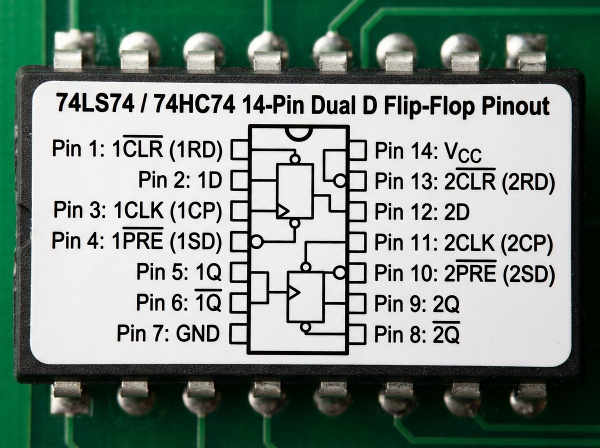
Synchronous Positive-Edge Triggering vs. Asynchronous Overrides
Understanding how synchronous and asynchronous inputs interact on the bench prevents misdiagnosing a working IC as defective:
Positive-Edge Clock Sampling: In both families, the logic level present at the Data () input is transferred to theoutput strictly on the low-to-high (rising) transition of the clock (). If you toggle theinput jumper between HIGH and LOW while the clock signal is sitting steady HIGH or steady LOW, theandoutputs will completely ignore the change until the exact rising edge of the next clock pulse arrives. Notably, Nexperia's 74HC74 and 74HCT74 incorporate Schmitt-trigger action on the clock () input, making the clock pin more tolerant of slower rise and fall times.
Active-Low Asynchronous Overrides (and): The Preset/Set and Clear/Reset pins are active-low—indicated by the overbar on the pinout diagram—and operate asynchronously. PullingLOW immediately forcesHIGH, while pullingLOW immediately forcesLOW, completely overpowering whatever the Data and Clock pins are doing. During normal synchronous operation, bothandmust be tied directly to the positive supply rail () so they remain inactive.
7474 74HC74 dual D type positive edged flip flops with clear and preset electronics demonstration
Design Boundary: The Simultaneous Active Set and Reset Unstable State
A critical boundary condition shared by both the 74LS74 and 74HC74 occurs when both asynchronous active-low inputs (and) are pulled LOW at the same time. As documented in STMicroelectronics' dual D flip-flop specification and analyzed in LTspice circuit simulation discussions, asserting both active-low overrides simultaneously forces bothandHIGH.
This temporary non-complementary state violates standardBoolean assumptions in downstream logic. Worse, this state does not persist once the inputs return HIGH: ifandare released tosimultaneously, an internal propagation race condition occurs, making the final latched state of the flip-flop unpredictable. Always design reset circuits so that only one asynchronous input can be asserted at any given instant.
Logic-Level Compatibility and Mixed-Family Interfacing (TTL vs. CMOS)
Interfacing between the 74LS74 and 74HC74 on a sharedsupply rail is strictly asymmetric. A 74HC74 CMOS output swings nearly rail-to-rail (fromto), which easily satisfies 74LS74 TTL input thresholds. Conversely, a 74LS74 bipolar totem-pole output drops voltage internally when sourcing a HIGH level, leaving its guaranteed minimum output voltage below the minimum input-high threshold required by a standard 74HC74 input.
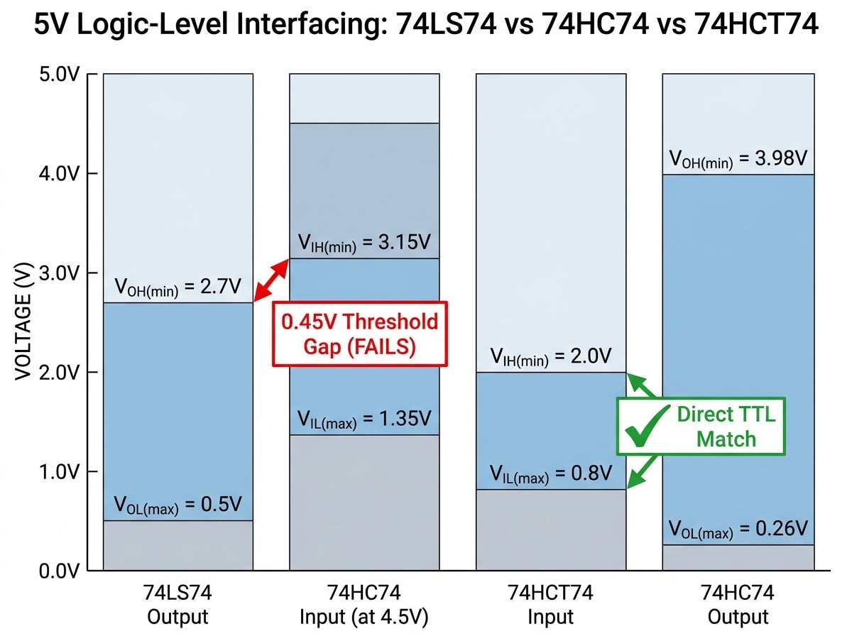
Driving 74LS74 Inputs from a 74HC74 Output (Directly Compatible at)
When a 74HC74 output drives a 74LS74 input on a sharedsupply (worst-case), the voltage levels align with generous noise margins:
According to the Texas Instruments SNx4HC74 datasheet, the CMOS output guarantees a minimum logic-high voltage () of (at) and (at)[1], while pulling its logic-low output () down to (at) or (at).
Meanwhile, the receiving 74LS74 input requires a minimum logic-high () of only and a maximum logic-low () of .
Becauseand, a 74HC74 output can directly drive several 74LS74 inputs without any level-shifting components.
Driving 74HC74 Inputs from a 74LS74 Output (ThetoThreshold Gap)
Reversing the signal direction—using a 74LS74 output to drive a 74HC74 input at—creates a classic hardware failure mode explained in ON Semiconductor Application Note AN-368 and Analog Devices Tutorial MT-098[8]:
Because the 74LS74 uses a bipolar Schottky totem-pole output stage with an upper Darlington/diode drop, its worst-case guaranteed logic-high output () atis only [2] (typically around).
However, a standard 74HC74 operating atproportions its CMOS input thresholds to the supply rail, demanding a minimum logic-high input () of (at, andat).
The Engineering Failure: The 74LS74's guaranteedoutput falls short of the 74HC74'sinput requirement. While a typicalunloaded TTL output might appear to work on a cool benchtop, any temperature drift, power-supply ripple, or bus noise can drop the signal into the indeterminate threshold region—causing missed clock edges, metastable latching, and increased CMOS shoot-through current.
Two Proven Fixes: External Pull-Up Resistors vs. Dropping in a 74HCT74
When a circuit requires aTTL output to drive a CMOS dual D flip-flop, engineers have two reliable solutions:
Add an External Pull-Up Resistor to: As explicitly noted in ON Semiconductor's 74HC74 documentation, 74HC74 inputs are directly compatible with standard CMOS outputs and—with external pull-up resistors connected to—compatible with LSTTL outputs. The resistor pulls the high-impedance CMOS gate all the way up to therail when the TTL totem-pole output turns off its lower sink transistor. When sizing the pull-up resistor, engineers must balance RC rise-time delay (against total bus capacitance) against the extra current the 74LS driver must sink () when pulling the line LOW.
Substitute a 74HCT74 (Preferred for PCB Repair): Soldering four to eight bodge resistors onto the underside of a dense logic board to pull up Data, Clock, Set, and Reset lines is impractical during repair. Dropping a 74HCT74 into the 14-pin socket solves the mismatch internally. The 74HCT74 uses the same low-power Si-gate CMOS core as the 74HC74, but shifts its input transistor geometry to guarantee TTL-compatible input thresholds (andacross atosupply).
Timing, Power Consumption, and Output Drive Comparison
Comparing the 74LS74 and 74HC74 across power, output drive, and switching speed highlights the architectural shift from current-driven bipolar logic to voltage-driven CMOS logic. While the 74HC74 offers a widertooperating envelope, microamp-level static current, and symmetrical output drive, the 74LS74 remains restricted tosystems with milliamp-level static current draw and sink-heavy asymmetric outputs.
Key Specifications Comparison Table (74LS74 vs. 74HC74 vs. 74HCT74)
| Specification / Parameter | 74LS74A (Low-Power Schottky TTL) | 74HC74 (High-Speed Si-Gate CMOS) | 74HCT74 (TTL-Compatible CMOS) |
|---|---|---|---|
| Semiconductor Technology | Bipolar Low-Power Schottky (LSTTL) | High-Speed Silicon-Gate CMOS | High-Speed Silicon-Gate CMOS |
| Operating Supply Voltage () | to(nom;–mil) | toWide Range | to(nom) |
| Input High / Low Thresholds () | (at) at;at | (at–) | |
| Output Voltage Swing () | (typ) /(at) | (at,) (at,) | Near Rail-to-Rail (to) |
| Output Current Drive () | Asymmetric:source /sink (mil) | Symmetrical:(at) (at) | Symmetrical:(at) |
| Quiescent Supply Current () | Continuous static draw:typ /max | Ultra-low static draw:max () com /mil | Ultra-low static draw (scales dynamically with clock frequency) |
| Max Clock Frequency (at) | min /typ (,) | min /typ (at) min /typ (at,) min /typ (at) | Comparable to 74HC74 at– |
| Setup () & Hold () Time | Verify in vendor AC table at | min (Data),min (inactive);(at) | Verify in vendor AC table at– |
Supply Voltage (), Quiescent Power Draw, and Temperature Grades
As highlighted in educational guides such as Build Electronic Circuits' 74HC74/74LS74 comparison and primary TI datasheets, the operating voltage window is the first dividing line between these ICs. The 74LS74 requiresnominal operation, whereas the 74HC74 runs fromto.
Power consumption follows an equally sharp divide:
Static vs. Dynamic Power: A bipolar 74LS74A draws continuous static bias current through its internal resistor networks whether the clock is running or halted—typically and up to maximum per dual package. By contrast, the TI SN74HC74 draws a maximum quiescent current () of just at(up toover the commercial temperature range andover the military range). As noted in ON Semiconductor AN-368, replacing LS logic with HC/HCT CMOS typically reduces active system power consumption by a factor of five or more[7].
Commercial vs. Military Temperature Grades: Both families split into commercial/industrial
74xxseries and military54xxseries. Per Texas Instruments SN54ALS74A and SN54LS74A documentation, 54-series devices are characterized for operation across the full military temperature range of to[3], whereas commercial 74LS74A devices are rated forto(and standard 74HC74 variants typically spantoor).
Output Drive Symmetry and Practical Load Protection
Bipolar TTL and CMOS output stages handle load current very differently:
Asymmetric 74LS74 Drive: A commercial 74LS74A output can sink up to in the LOW state (for military 54LS74A), but can only source in the HIGH state. Because of this 20-to-1 asymmetry, classic TTL circuit designers almost always wire indicator LEDs and optocouplers active-low (betweenand the output pin) so the flip-flop sinks the load current.
Symmetrical 74HC74 Drive & LED Resistor Sizing: The 74HC74 features a complementary P-channel/N-channel MOSFET output stage that sources and sinks current symmetrically: atand at.
Practical Bench Rule: Because a 74HC74 output has a strictcontinuous rating at–(far lower than a 555 timer or dedicated buffer), driving an indicator LED with a standardorresistor on abreadboard will overload the output stage and pullout of spec. Always protect 74HC74 output LEDs on arail with at least a current-limiting resistor, which keeps the LED current safely down around –.
Why Timing Rankings, Distributor Blogs, and AI Answers Disagree (andScaling)
If you search online for whether the 74LS74 or 74HC74 is faster, you will encounter contradictory claims—including garbled component broker tables that simultaneously label 74LS as "faster than HC" and "slower compared to LS."
In reality, Official datasheet specifications from Philips/NXP (hosted via NJIT), Renesas HD74HC Application Notes, and Texas Instruments show why single-number speed comparisons are misleading:
CMOS Speed Scales Dramatically with: A 74LS74A is only specified at(), where it guarantees a minimum maximum clock frequency () of (typical). By contrast, a 74HC74's switching speed depends heavily on supply voltage. At, the SN74HC74 is much slower than LSTTL, dropping tomin (typ). However, when powered atto, the SN74HC74 accelerates to –min (–typ)—outpacing the 74LS74A.
Capacitive Load Test Conditions (vs.): Historical LSTTL datasheets measured propagation delay () andinto a light test load. Modern 74HC74 datasheets often publish standard AC tables at alongsidereference figures[5] (as seen in the Philips/NXP 74HC/HCT74 datasheet). Comparing a 74HC74 rated at(or) against a 74LS74A rated atandcreates a false impression that CMOS is slower. Atunder matching capacitive loads, high-speed Si-gate CMOS matches or exceeds LSTTL speed.
Application Boundaries: Best-For Scenarios, Sourcing Notes, and Who Should Avoid Each
Selecting between the 74LS74, 74HC74, and 74HCT74 comes down to matching the IC's input/output stage to your power rail and surrounding logic family. Choose the 74LS74 to preserve authentic bipolar electrical loading in legacyTTL equipment, choose the 74HC74 for new CMOS designs operating betweenand, and choose the 74HCT74 whenever a low-power CMOS replacement must interface directly withTTL signals.
Option 1: 74LS74 / 74LS74A (Low-Power Schottky TTL)
Best For: Authentic board-level repair of vintageTTL hardware—such as 1970s/1980s arcade logic boards, industrial CNC controllers, and retrocomputing buses—where originallow-state sink drive and bipolar propagation characteristics are expected.
Strengths: Naturally immune to electrostatic gate-oxide breakdown compared to unbuffered CMOS; stronglow-side current sinking; inputs do not oscillate as violently as high-impedance CMOS if briefly left unconnected during bench testing (though tying unused pins remains mandatory for noise immunity).
Drawbacks: Restricted to a narrow–supply window; continuous–static current draw per IC;minimumcannot drive 74HC CMOS inputs directly.
Who Should NOT Choose 74LS74: Engineers designingmicrocontroller peripherals, battery-powered portable devices, or pure CMOS logic boards.
Option 2: 74HC74 (High-Speed Silicon-Gate CMOS)
Best For: New digital hardware designs, battery-operated equipment,ormicrocontroller interfaces (ESP32, STM32, AVR, PIC), and pure CMOS state machines.
Strengths: Widetosupply range; negligiblemax static current at room temperature; symmetricaltorail-to-rail output drive; superior noise immunity in pure CMOS circuits.
Drawbacks: High-impedance inputs oscillate wildly if left floating;(at) fails to reliably readTTL outputs without external pull-up resistors.
Who Should NOT Choose 74HC74: Repair technicians performing a direct, unbuffered drop-in replacement on a legacyTTL circuit board where upstream 74LS gates drive the flip-flop.
Option 3: 74HCT74 (TTL-Input-Compatible High-Speed CMOS Bridge)
Best For: Drop-in replacement of a dead 74LS74 on aPCB, or unidirectional level-shifting fromCMOS /TTL outputs () into aCMOS subsystem.
Strengths: Accepts TTL input levels (,) while outputting full rail-to-railCMOS levels at microamp quiescent power.
Drawbacks: Restricted to atosupply window; exhibits slightly higher shoot-through current than 74HC when driven by lower-voltage TTL high levels (–).
Who Should NOT Choose 74HCT74: Designers working onorpower rails, where 74HCT devices are outside their rated supply window.
Sourcing, Package Suffixes, and Counterfeit Avoidance
When ordering replacements for production or bench stock, verify the complete manufacturer part number suffix:
Package Footprint: Standard through-hole 14-pin dual in-line packages use the
Nsuffix in Texas Instruments nomenclature (e.g.,SN74LS74AN,SN74HC74N), while surface-mount 14-pin SOIC packages useD(SN74HC74D/74HC74D) and TSSOP packages usePW(74HC74PW).Sourcing Precaution: Always source from authorized semiconductor distributors with traceable manufacturer datasheets. Remarked surplus chips—where a standard
74HC74is laser-etched as a74LS74or74HCT74—will immediately cause threshold failures inTTL sockets.
Common Repair & Design Mistakes (Hidden Risks on PCBs and Breadboards)
Most erratic flip-flop behavior encountered during board repair or breadboard prototyping traces back to four physical mistakes: leaving unused high-impedance CMOS inputs floating on legacy TTL pads, exceeding maximum clock rise/fall times, omitting localbypass capacitors, or mixing 74LS and 74HC chips across unbuffered breadboard buses.
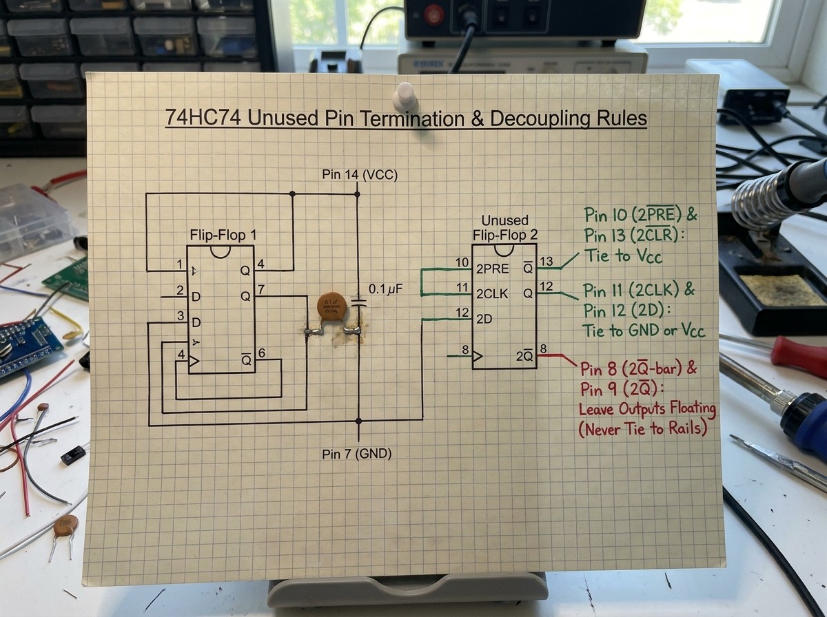
1. The "Floating Input" Trap on Unused Flip-Flop Pins
Because the 74xx74 houses two independent flip-flops in a single 14-pin package, schematics frequently use only one half of the IC (for example, Flip-Flop 1 on pins 1–6) as a frequency divider or latch, leaving Flip-Flop 2 (pins 8–13) unused. On older 74LS74 boards, designers occasionally left unused pins unconnected because bipolar TTL inputs tend to float HIGH internally (though explicit termination is always recommended).
If you solder a 74HC74 into a socket with unconnected input pads, its high-impedance CMOS inputs act as tiny antennas that pick up stray electromagnetic noise. The unused flip-flop will oscillate at megahertz frequencies, bias both P-channel and N-channel transistors into linear conduction (shoot-through), overheat the package, and corrupt the active flip-flop through internal ground bounce.
The Exact Bench Termination Rule:
As mandated in Section 8.3 of the Texas Instruments SNx4HC74 datasheet and Renesas HD74HC Application Note:
Tie All Unused Inputs to Fixed Rails: When Flip-Flop 2 (pins 8–13) is unused, tie its active-low asynchronous pins (on Pin 13 andon Pin 10) to, and tie its synchronous inputs (on Pin 11 andon Pin 12) directly toor.
Leave Unused Outputs Floating: Never tie unused output pins (on Pin 9 andon Pin 8) toor, as doing so creates a direct short circuit against the output driver. TI explicitly specifies: "Unused outputs can be left floating. Do not connect outputs directly toor ground."
2. Missing LocalDecoupling Capacitors
High-speed CMOS outputs switch states with sharp voltage edges () and transient current spikes. The TI SNx4HC74 datasheet states that eachterminal should have a local bypass capacitor (typically aceramic capacitor) placed as close to Pin 14 and Pin 7 as possible to prevent power-rail droop from falsely triggering the asynchronous Clear or Preset lines.
3. Slow Clock Edges and Breadboard Bus Mixing (Ben Eater / 65c02 / Arduino)
In real-world prototyping threads on Electronics Stack Exchange (Ben Eater 8-bit breadboard computer) and the Arduino Forum, builders frequently report that swapping a 74HC74 and 74LS74 causes missing square waves, double-clocking, or unexpected state changes. Alongside thevs.threshold mismatch, slow input transition times () are a major culprit: standard SN74HC74 inputs require rise and fall times faster than at (at;at). Driving a clock pin from a slow RC network or a heavily loaded 555 timer without a Schmitt-trigger buffer can cause the flip-flop to oscillate or double-trigger right at the threshold crossing.
Diagnostic Troubleshooting Table
| Observed Circuit Symptom | Probable Root Cause | Engineering Fix |
|---|---|---|
| Flip-flop state changes randomly or IC runs warm after replacing 74LS74 with 74HC74 | Unused inputs on the active or spare flip-flop (pins 10–13) are left floating on the PCB or breadboard. | Tie all unused input pins () toor; leave unusedoutput pins unconnected. |
| Missing pulses or altered square-wave output when swapping 74HC74 and 74LS74 | 74LS output () failing to cross 74HC input threshold (), or output overloaded by low-value LED resistor. | Add a pull-up resistor toon TTL-to-CMOS lines, or replace 74HC74 with 74HCT74; useseries resistors onCMOS output LEDs. |
| Double-clocking or false triggers when adjacent gates switch | Missing localbypass capacitor, or clock rise/fall time exceeding thelimit (at). | Place aceramic bypass capacitor directly across Pin 14 () and Pin 7 (); use a Schmitt-trigger clock buffer or Nexperia 74HC74 variant. |
| Bothandoutputs go HIGH simultaneously or latch randomly after reset | Both active-low(Preset) and(Clear) pulled LOW at the same time. | Tie inactivesolidly toso onlypulses LOW during power-on reset, avoiding simultaneous assertion. |
Pre-Implementation & Board-Repair Verification Checklist
Before soldering a replacement IC into a logic board or locking a bill of materials (BOM) for production, run through this six-point engineering checklist against your schematic and manufacturer datasheet:
1. Verify Exact OperatingTolerance: Confirm with a multimeter whether the supply rail is a regulatedsystem (–for commercial 74LS74A;–for 74HCT74) or a wider–/rail requiring the 74HC74.
2. Audit Worst-Casevs.andvs.Margins: Check the DC Electrical Characteristics table of every upstream driver and downstream receiver. If anybipolar TTL output () feeds the flip-flop, specify a 74HCT74 () or include external pull-up resistors to.
3. Check AC Timing () at Your Actual Load Capacitance (): Verify that setup time (min for data,min forrecovery on SN74HC74 at), hold time (), and propagation delay meet your clock budget at the capacitive load (vs.) andvoltage matching your board.
4. Confirm Output Sink/Source Current () Against Load Demand: Ensure downstream loads do not exceed(at) on a 74HC74/74HCT74, orhigh-side source /low-side sink on a commercial 74LS74A. Sizeindicator LED resistors at() for CMOS outputs.
5. Inspect Termination of All Unused Inputs (Pins 1–4 and 10–13): Verify on the physical PCB that active-lowandare tied towhen unused, and that all four inputs () of an unused flip-flop half are tied toor, while leaving unusedandoutputs floating.
6. Confirm LocalBypass Capacitance & Input Transition Times: Ensure a local decoupling capacitor is installed close to Pin 14 () and verify that clock/data rise and fall times stay below(at) for standard CMOS inputs.
Frequently Asked Questions (74LS74 vs 74HC74)
What is the technical name of the 74LS74 and 74HC74 IC, and what logic function does a 7474 perform?
Both the 74LS74 and 74HC74 are officially designated as Dual D-Type Positive-Edge-Triggered Flip-Flops with Preset (Set) and Clear (Reset). Each 14-pin integrated circuit contains two independent 1-bit sequential memory elements used for data latching, frequency division (wiringback tofor divide-by-2 clock scaling), shift registers, and synchronous state machines.
Can I replace a 74LS74 with a 74HC74 directly?
Only conditionally. Although both share an identical 14-pin layout, a standard 74HC74 installed in aTTL circuit will fail to reliably recognize logic-high outputs from upstream 74LS gates (vs.at) unless you add external pull-up resistors to. Furthermore, any unused input pins left floating on an older TTL board will cause the 74HC74 to oscillate. For a true drop-in replacement of a 74LS74 on aboard, use a 74HCT74.
Can a 74HC74 drive a 74LS74 directly without level shifting?
Yes, when both ICs operate on a sharedsupply rail. At, a 74HC74 CMOS output swings up to at least(at) and down to(at), which easily satisfies theandinput thresholds of a 74LS74 within the CMOS output'scurrent rating.
Why should I use a 74HCT74 instead of a 74HC74 in a 5V TTL circuit?
The 74HCT74 combines a low-power Silicon-Gate CMOS core with a TTL-compatible input stage (,across atosupply). This allows it to read74LS/TTL outputs directly without requiring external pull-up resistors soldered onto the PCB.
What happens if I leave unused pins floating on a 74HC74 versus a 74LS74?
Leaving unused input pins () floating on a CMOS 74HC74 causes high-frequency noise pickup, unpredictable output oscillation, and high shoot-through supply current. All unused inputs on both flip-flops in the 14-pin package must be tied directly toor, whereas unusedandoutput pins must be left unconnected.
Sources and references used for this guide
SNx4HC74 Dual D-Type Positive-Edge-Triggered Flip- ...
Source type: official company documentation
Used for: Supports 74HC74 supply voltage rating rules and the requirement that each VCC terminal should have a local bypass capacitor.
Caution: Official manufacturer datasheet; snippet does not expose full numerical DC/AC tables, so avoid inventing unverified numbers.Triggered Flip-Flops With Preset And Clear datasheet
Source type: official company documentation
Used for: Supports official SN74LS74A dual positive-edge-triggered D flip-flop architecture with asynchronous preset and clear.
Caution: Official manufacturer datasheet; verify exact switching and threshold parameters directly in the PDF before citing specific numbers.SN54ALS74A
Source type: official company documentation
Used for: Supports military temperature range characterization (-55°C to 125°C) for 54-series variants and ICC measurement conditions.
Caution: Covers 54ALS/AS military family documentation; do not conflate ALS switching speeds with standard 74LS74A limits.74HC74 Dual D Flip−Flop with Set and Reset
Source type: official company documentation
Used for: Proves that the 74HC74 is identical in pinout to the LS74, directly compatible with standard CMOS outputs, and compatible with LSTTL outputs when pull-up resistors are used.
Caution: Official ON Semiconductor datasheet hosted on Mouser; snippet truncates before specifying exact pull-up resistor values.74HC/HCT74 Dual D-type flip-flop with set and reset
Source type: official company documentation
Used for: Supports that 74HC/HCT74 are high-speed Si-gate CMOS devices pin-compatible with LSTTL, with propagation delay characterized at CL = 15 pF.
Caution: Authoritative university-hosted Philips datasheet; use cautiously within the bounds of the extracted snippet.74HC74; 74HCT74
Source type: official company documentation
Used for: Confirms dual positive-edge-triggered D-type flip-flop architecture with individual data (nD), clock (nCP), set (nSD), and reset (nRD) inputs for both 74HC74 and 74HCT74.
Caution: Official Nexperia datasheet; use for functional architecture and 74HCT74 drop-in alternative context.Application Note 368 An Introduction to and Comparison of ...
Source type: official company documentation
Used for: Supports engineering comparison methodology between 74HC, 74HCT, and bipolar TTL logic families.
Caution: Official ON Semiconductor application note; use for family-level interfacing principles.MT-098: Low Voltage Logic Interfacing
Source type: official company documentation
Used for: Supports fundamental TTL-to-CMOS and CMOS-to-TTL voltage threshold interfacing rules and noise margin concepts.
Caution: Official Analog Devices tutorial; apply to general logic-level compatibility boundaries.
Specifications
 2N5551 Transistor: Pinout, Datasheet, and Applications
09 July 202114708
 ATtiny13A 8-Bit Microcontroller: Datasheet, Specifications, Pinout
28 September 20217977
 Unveiling the PIC16CE62X OTP 8-bit CMOS MCU with EEPROM Data Memory: Technical Deep Dive
29 February 2024544
![How to Run IRFP250 Transistor Safely? [FAQ& Video]](https://res.utmel.com/Images/Article/baa907de-272a-42c4-8930-aa53614d9c2d.jpg) How to Run IRFP250 Transistor Safely? [FAQ& Video]
How to Run IRFP250 Transistor Safely? [FAQ& Video]25 April 20225781
 AT89S8253 Microcontroller: Pinout, Equivalent and Datasheet
25 February 20223734
 BD437 Transistor: BD437 Pinout, Datasheet, Equivalent
06 April 20224198
 MCP3008 IC: Datasheet, Pinout, Specifications
27 August 202113259
 SAM-M8Q:u-blox M8 GNSS antenna module
09 March 20222016
 How New Battery Charger Technology is Shaping the Future
10 July 20251308
 How to Select a Power Relay That Fits Your Requirements
10 July 20252979
 What is speaker?
08 October 20218987
 Weak Current Control Strong Current: How to use the Relay?
28 November 20226870
 Circuit Breaker: Working Principle, Types and Structure
21 November 202512344
 Tough Times for Japanese Component Manufacturers
10 August 20223090
 Humanoid Robot BOM Breakdown: Every Chip Inside a Physical AI Platform
28 July 20261704
 Introduction to BGA Package
07 December 20216420
Rochester Electronics
In Stock
United States
China
Canada
Japan
Russia
Germany
United Kingdom
Singapore
Italy
Hong Kong(China)
Taiwan(China)
France
Korea
Mexico
Netherlands
Malaysia
Austria
Spain
Switzerland
Poland
Thailand
Vietnam
India
United Arab Emirates
Afghanistan
Åland Islands
Albania
Algeria
American Samoa
Andorra
Angola
Anguilla
Antigua & Barbuda
Argentina
Armenia
Aruba
Australia
Azerbaijan
Bahamas
Bahrain
Bangladesh
Barbados
Belarus
Belgium
Belize
Benin
Bermuda
Bhutan
Bolivia
Bonaire, Sint Eustatius and Saba
Bosnia & Herzegovina
Botswana
Brazil
British Indian Ocean Territory
British Virgin Islands
Brunei
Bulgaria
Burkina Faso
Burundi
Cabo Verde
Cambodia
Cameroon
Cayman Islands
Central African Republic
Chad
Chile
Christmas Island
Cocos (Keeling) Islands
Colombia
Comoros
Congo
Congo (DRC)
Cook Islands
Costa Rica
Côte d’Ivoire
Croatia
Cuba
Curaçao
Cyprus
Czechia
Denmark
Djibouti
Dominica
Dominican Republic
Ecuador
Egypt
El Salvador
Equatorial Guinea
Eritrea
Estonia
Eswatini
Ethiopia
Falkland Islands
Faroe Islands
Fiji
Finland
French Guiana
French Polynesia
Gabon
Gambia
Georgia
Ghana
Gibraltar
Greece
Greenland
Grenada
Guadeloupe
Guam
Guatemala
Guernsey
Guinea
Guinea-Bissau
Guyana
Haiti
Honduras
Hungary
Iceland
Indonesia
Iran
Iraq
Ireland
Isle of Man
Israel
Jamaica
Jersey
Jordan
Kazakhstan
Kenya
Kiribati
Kosovo
Kuwait
Kyrgyzstan
Laos
Latvia
Lebanon
Lesotho
Liberia
Libya
Liechtenstein
Lithuania
Luxembourg
Macao(China)
Madagascar
Malawi
Maldives
Mali
Malta
Marshall Islands
Martinique
Mauritania
Mauritius
Mayotte
Micronesia
Moldova
Monaco
Mongolia
Montenegro
Montserrat
Morocco
Mozambique
Myanmar
Namibia
Nauru
Nepal
New Caledonia
New Zealand
Nicaragua
Niger
Nigeria
Niue
Norfolk Island
North Korea
North Macedonia
Northern Mariana Islands
Norway
Oman
Pakistan
Palau
Palestinian Authority
Panama
Papua New Guinea
Paraguay
Peru
Philippines
Pitcairn Islands
Portugal
Puerto Rico
Qatar
Réunion
Romania
Rwanda
Samoa
San Marino
São Tomé & Príncipe
Saudi Arabia
Senegal
Serbia
Seychelles
Sierra Leone
Sint Maarten
Slovakia
Slovenia
Solomon Islands
Somalia
South Africa
South Sudan
Sri Lanka
St Helena, Ascension, Tristan da Cunha
St. Barthélemy
St. Kitts & Nevis
St. Lucia
St. Martin
St. Pierre & Miquelon
St. Vincent & Grenadines
Sudan
Suriname
Svalbard & Jan Mayen
Sweden
Syria
Tajikistan
Tanzania
Timor-Leste
Togo
Tokelau
Tonga
Trinidad & Tobago
Tunisia
Turkey
Turkmenistan
Turks & Caicos Islands
Tuvalu
U.S. Outlying Islands
U.S. Virgin Islands
Uganda
Ukraine
Uruguay
Uzbekistan
Vanuatu
Vatican City
Venezuela
Wallis & Futuna
Yemen
Zambia
Zimbabwe
![27C64-20/SO]() 27C64-20/SO
27C64-20/SORochester Electronics
![27C64-15/SO]() 27C64-15/SO
27C64-15/SORochester Electronics
![24C04AT/SN]() 24C04AT/SN
24C04AT/SNRochester Electronics
![27C128-250]() 27C128-250
27C128-250Rochester Electronics
![27C256-25]() 27C256-25
27C256-25Rochester Electronics
![2764A-2]() 2764A-2
2764A-2Rochester Electronics
![29F53SDC]() 29F53SDC
29F53SDCRochester Electronics
![27128A]() 27128A
27128ARochester Electronics
![27S13APCTB]() 27S13APCTB
27S13APCTBRochester Electronics
![2N3415_NL]() 2N3415_NL
2N3415_NLRochester Electronics