
AD600: Datasheet, Pinout, and Ultrasound Imaging Guide

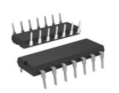
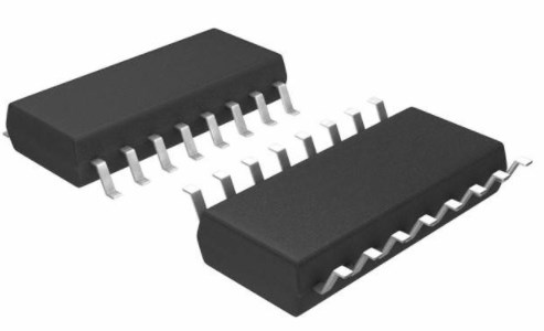
50mA per Channel 350nA 30 dB Instrumentational OP Amps ±4.75V~5.25V AD600 16 Pins 16-SOIC (0.295, 7.50mm Width)


50mA per Channel 350nA 30 dB Instrumentational OP Amps ±4.75V~5.25V AD600 16 Pins 16-SOIC (0.295, 7.50mm Width)
The AD600 is a dual, low-noise Variable Gain Amplifier (VGA) by Analog Devices, essential for ultrasound and AGC. Explore specs, pinouts, and design alternatives.
- Executive Summary: What is the AD600?
- 1. Technical Specifications & Performance Analysis
- 2. Pinout, Package, and Configuration
- 3. Design & Integration Guide (For Engineers & Makers)
- 4. Typical Applications & Use Cases
- 5. Alternatives and Cross-Reference Guide
- 6. Frequently Asked Questions (FAQ)
- 7. Datasheets & Resources
- Specifications
- Datasheet PDF
Executive Summary: What is the AD600?
The AD600 is a dual-channel, low-noise Variable Gain Amplifier (VGA) manufactured by Analog Devices, featuring a linear-in-dB gain control system designed for precision signal processing.
Market Position: High-performance analog component; industry standard for commercial and medical instrumentation.
Top Features: Dual independent channels, ultra-low input noise (1.4 nV/√Hz), and a massive 80 dB cascaded gain range.
Primary Audience: Ideal for Biomedical Engineers (Ultrasound), RF Designers, and Instrumentation specialists.
Supply Status: Active (Refer to official distributors for real-time stock).
1. Technical Specifications & Performance Analysis
1.1 Core Architecture (CPU/Logic/Power)
The AD600 utilizes a proprietary circuit architecture to achieve a linear-in-dB gain response, which is crucial for applications requiring wide dynamic range compression. Unlike standard op-amps, the gain is controlled linearly by a voltage interface, making it the "brain" of Automatic Gain Control (AGC) loops. The dual-channel design allows for cascaded operation to achieve up to 80 dB of gain or independent operation for stereo/dual-signal processing.
1.2 Key Electrical Characteristics
This VGA is engineered for sensitive signal chains where noise performance is critical.
Input Noise: 1.4 nV/√Hz (at 1 MHz) – Essential for detecting weak signals in ultrasound.
Bandwidth: 35 MHz (-3 dB point), suitable for video and IF signal processing.
Gain Range: 0 dB to 40 dB per channel (up to 80 dB when cascaded).
Supply Voltage: Operating range of ±4.75 V to ±5.25 V (Nominal ±5 V).
Gain Accuracy: ±0.5 dB, ensuring precise calibration in measurement tools.
1.3 Interfaces and Connectivity
The AD600 interfaces primarily through analog voltage control.
Gain Control Interface: High-impedance differential inputs tailored for easy drive by D/A converters or analog control loops.
Signal I/O: Differential inputs and single-ended outputs.
Impedance: Laser-trimmed input resistance for consistent matching.
2. Pinout, Package, and Configuration
2.1 Pin Configuration Guide
The AD600 generally utilizes a 16-pin configuration to support its dual-channel architecture.
Power Pins: VPOS (+5V), VNEG (-5V) – Requires clean, decoupled power.
Inputs (Ch 1/2): A1HI, A1LO, A2HI, A2LO – Differential signal inputs.
Outputs (Ch 1/2): OUT1, OUT2 – Signal outputs.
Gain Control: C1HI, C1LO, C2HI, C2LO – Determines the amplification level.
Gate: Used to gate the channel off (if applicable to specific variant).
2.2 Naming Convention & Ordering Codes
Understanding the Part Numbers:analog Devices uses specific suffixes to denote package and environmental grades.
AR/ARZ: Indicates SOIC (Small Outline Integrated Circuit). The 'Z' denotes RoHS Compliant (Lead-Free).
SQ: Indicates CDIP (Ceramic Dual In-line Package), typically for military or high-temp industrial use.
2.3 Available Packages
| Package Type | Dimensions | Common Use Case |
|---|---|---|
| AD600AR/ARZ | 16-Lead SOIC | Standard commercial PCBs, surface mount. |
| AD600SQ | 16-Lead CDIP | Hermetically sealed for harsh environments. |
| AD602AR | 16-Lead SOIC | Variant with shifted gain range (-10 to +30 dB). |
3. Design & Integration Guide (For Engineers & Makers)
Pro Tip: When designing with high-gain amplifiers like the AD600, PCB layout is critical to prevent oscillation and noise coupling.
3.1 Hardware Implementation
Bypass Capacitors: Essentials: Place 0.1 µF ceramic capacitors in parallel with 4.7 µF tantalum capacitors as close as possible to the VPOS and VNEG pins to filter power supply noise.
PCB Layout: Use a solid ground plane. Keep the input and output traces separated to avoid feedback oscillation, especially given the 35 MHz bandwidth.
Thermal Management: While standard operation (±5V) rarely requires a heatsink, ensure adequate airflow in dense enclosures.
3.2 Common Design Challenges
Gain Control Ripple: - Issue: Noise on the gain control voltage inputs (C1HI/C1LO) directly modulates the signal, creating artifacts. - Fix: Use heavy filtering on the control voltage lines or precision DACs for gain setting.
Crosstalk in Dual Channels: - Issue: At high frequencies (near 35 MHz), signal leakage can occur between Channel 1 and Channel 2. - Fix: Use guard traces between channel inputs on the PCB and ensure the power supply impedance is low.
4. Typical Applications & Use Cases
4.1 Real-World Example: Ultrasound Time-Gain Compensation (TGC)
In medical ultrasound, signals return from deeper tissue significantly weaker than surface reflections. The AD600 is used in Time-Gain Compensation circuits. As the return signal delay increases (indicating depth), the control voltage to the AD600 is ramped up linearly. This compensates for attenuation, normalizing the image brightness across the depth of the scan.
5. Alternatives and Cross-Reference Guide
Direct Replacements:
For exact pin compatibility, check the AD602 (same family, different gain range).
Competitor Options:
Texas Instruments VCA821/VCA824: Wideband variable gain amplifiers often used in similar video and RF applications. Check bandwidth specs as VCA series often offer higher BW (up to 420 MHz) but different gain scaling.
Maxim Integrated MAX2039: Tailored for mixer/VGA applications in basestations, though pinout differs.
Cost-Effective Options:
For lower frequency or less precise applications, standard Operational Transconductance Amplifiers (OTAs) like the LM13700 can be configured for VCA usage, but with significantly higher noise and lower bandwidth.
6. Frequently Asked Questions (FAQ)
Q: What is the primary difference between AD600 and AD602?
A: The AD600 has a gain range of 0 dB to 40 dB per channel. The AD602 is optimized for lower gains, ranging from -10 dB to +30 dB per channel, to handle larger input signals without clipping.
Q: Can the AD600 be used for audio applications?
A: Yes, its low noise (1.4 nV/√Hz) makes it excellent for high-end audio dynamic range compression, though its bandwidth is overkill for standard audio.
Q: How do I control the gain digitally?
A: You cannot control it directly via SPI/I2C. You must use a DAC (Digital-to-Analog Converter) to provide a control voltage to the gain interface pins.
Q: Is the AD600 suitable for battery-operated devices?
A: It consumes moderate power (approx. ±5V supply). While possible, modern low-power CMOS alternatives might be better for strictly battery-constrained IoT devices.
7. Datasheets & Resources
Official Datasheet: AD600/AD602 Data Sheet (Mouser)
Development Tools: Look for generic VGA evaluation boards or the AD600-EVALZ if available.
Specifications
Datasheet PDF
- PCN Obsolescence/ EOL :
- Datasheets :
- ConflictMineralStatement :
 LT1014 Quad Precision Op-Amp: Pinout, Datasheet, Circuit
19 November 20211653
 A Comprehensive Guide to LTC6947IUFD#TRPBF PLL Frequency Synthesizer
06 March 2024300
 KSZ9031RNXCA Transceiver Full Ethernet 48-QFN: KSZ9031RNXCA VS KSZ9021RNI, and Equivalents
15 February 2022574
 TL431CD Programmable Voltage Reference: Pinout, Features, and Datasheet
15 May 20211527
 BAT54S Diode: BAT54S Datasheet, Price, Pinout
27 January 20223688
 An In-Depth Look at the LTC6602IUF#TRPBF Active Filter: Features, Applications, and Reference Designs
06 March 2024111
 74LS47: Driver, Pinout, Circuit And Equivalents
30 March 20225380
 A Comprehensive Guide to LTC6995CS6-2#TRPBF Programmable Timer and Oscillator
06 March 2024244
 Voltage Regulator: Types, Working, and Applications
23 February 202122544
 Classification and Working Principle of Ballast Resistor
18 November 20205612
 Insulation Approaches for Power Electronic Converters
12 October 20232595
 What is RF Switch?
16 November 20215439
 How to Understand the Oscilloscope Bandwidth?
13 December 20218495
 What is a Tactile Sensor?
21 October 20213623
 What is a DC-to-DC Converter?
23 April 20216682
 What is a Resistor Used For?
01 August 20251212
Analog Devices Inc.
In Stock
United States
China
Canada
Japan
Russia
Germany
United Kingdom
Singapore
Italy
Hong Kong(China)
Taiwan(China)
France
Korea
Mexico
Netherlands
Malaysia
Austria
Spain
Switzerland
Poland
Thailand
Vietnam
India
United Arab Emirates
Afghanistan
Åland Islands
Albania
Algeria
American Samoa
Andorra
Angola
Anguilla
Antigua & Barbuda
Argentina
Armenia
Aruba
Australia
Azerbaijan
Bahamas
Bahrain
Bangladesh
Barbados
Belarus
Belgium
Belize
Benin
Bermuda
Bhutan
Bolivia
Bonaire, Sint Eustatius and Saba
Bosnia & Herzegovina
Botswana
Brazil
British Indian Ocean Territory
British Virgin Islands
Brunei
Bulgaria
Burkina Faso
Burundi
Cabo Verde
Cambodia
Cameroon
Cayman Islands
Central African Republic
Chad
Chile
Christmas Island
Cocos (Keeling) Islands
Colombia
Comoros
Congo
Congo (DRC)
Cook Islands
Costa Rica
Côte d’Ivoire
Croatia
Cuba
Curaçao
Cyprus
Czechia
Denmark
Djibouti
Dominica
Dominican Republic
Ecuador
Egypt
El Salvador
Equatorial Guinea
Eritrea
Estonia
Eswatini
Ethiopia
Falkland Islands
Faroe Islands
Fiji
Finland
French Guiana
French Polynesia
Gabon
Gambia
Georgia
Ghana
Gibraltar
Greece
Greenland
Grenada
Guadeloupe
Guam
Guatemala
Guernsey
Guinea
Guinea-Bissau
Guyana
Haiti
Honduras
Hungary
Iceland
Indonesia
Iran
Iraq
Ireland
Isle of Man
Israel
Jamaica
Jersey
Jordan
Kazakhstan
Kenya
Kiribati
Kosovo
Kuwait
Kyrgyzstan
Laos
Latvia
Lebanon
Lesotho
Liberia
Libya
Liechtenstein
Lithuania
Luxembourg
Macao(China)
Madagascar
Malawi
Maldives
Mali
Malta
Marshall Islands
Martinique
Mauritania
Mauritius
Mayotte
Micronesia
Moldova
Monaco
Mongolia
Montenegro
Montserrat
Morocco
Mozambique
Myanmar
Namibia
Nauru
Nepal
New Caledonia
New Zealand
Nicaragua
Niger
Nigeria
Niue
Norfolk Island
North Korea
North Macedonia
Northern Mariana Islands
Norway
Oman
Pakistan
Palau
Palestinian Authority
Panama
Papua New Guinea
Paraguay
Peru
Philippines
Pitcairn Islands
Portugal
Puerto Rico
Qatar
Réunion
Romania
Rwanda
Samoa
San Marino
São Tomé & Príncipe
Saudi Arabia
Senegal
Serbia
Seychelles
Sierra Leone
Sint Maarten
Slovakia
Slovenia
Solomon Islands
Somalia
South Africa
South Sudan
Sri Lanka
St Helena, Ascension, Tristan da Cunha
St. Barthélemy
St. Kitts & Nevis
St. Lucia
St. Martin
St. Pierre & Miquelon
St. Vincent & Grenadines
Sudan
Suriname
Svalbard & Jan Mayen
Sweden
Syria
Tajikistan
Tanzania
Timor-Leste
Togo
Tokelau
Tonga
Trinidad & Tobago
Tunisia
Turkey
Turkmenistan
Turks & Caicos Islands
Tuvalu
U.S. Outlying Islands
U.S. Virgin Islands
Uganda
Ukraine
Uruguay
Uzbekistan
Vanuatu
Vatican City
Venezuela
Wallis & Futuna
Yemen
Zambia
Zimbabwe
![AD826AR-REEL7]() AD826AR-REEL7
AD826AR-REEL7Analog Devices Inc.
![AD8062ARM]() AD8062ARM
AD8062ARMAnalog Devices Inc.
![AD8532ARU-REEL]() AD8532ARU-REEL
AD8532ARU-REELAnalog Devices Inc.
![OP113ES]() OP113ES
OP113ESAnalog Devices Inc.
![SSM2142P]() SSM2142P
SSM2142PAnalog Devices, Inc.
![LTC1050CS8]() LTC1050CS8
LTC1050CS8Linear Technology/Analog Devices
![AMP02EPZ]() AMP02EPZ
AMP02EPZAnalog Devices Inc.
![AD822ARZ-REEL7]() AD822ARZ-REEL7
AD822ARZ-REEL7Analog Devices Inc.
![OP2177ARZ-REEL7]() OP2177ARZ-REEL7
OP2177ARZ-REEL7Analog Devices Inc.
![AD8066ARZ-R7]() AD8066ARZ-R7
AD8066ARZ-R7Analog Devices Inc.


