

 Product
 Brand
Brand Articles
 Tools
Tools
INA121 Instrumentation Amplifier: FET-Input Design Notes, SPICE Troubleshooting, and Alternatives

4pA Instrumentational OP Amps 4.5V~36V ±2.25V~18V INA121 8-SOIC (0.154, 3.90mm Width)


4pA Instrumentational OP Amps 4.5V~36V ±2.25V~18V INA121 8-SOIC (0.154, 3.90mm Width)
Discover technical design notes for the INA121 FET-input instrumentation amplifier. Learn how to manage its 4pA bias current, fix SPICE simulation errors, and compare alternatives.
- Core Architecture: Why the INA121’s FET-Input Matters
- Electrical Specification Breakdown for System Design
- Resolving SPICE Simulation Errors and "Floating Pin" Traps
- Managing Offset Voltage and Saturation Anomalies
- High-Impedance Sensor Applications in Practice
- Footprint, Pinout, and Datasheet Verification
- Evaluating Alternatives and Replacement Options
- Frequently Asked Questions
- Specifications
- Datasheet PDF
The INA121 is a FET-input, low-power instrumentation amplifier designed for high-impedance sensor applications, offering excellent accuracy and extremely low input bias current.
For design engineers and procurement managers dealing with precision analog front-ends, the choice between a standard bipolar instrumentation amplifier and a FET-input device dictates the entire trajectory of the sensor interface design. The INA121 occupies a highly specific niche: it provides the high common-mode rejection expected of a classic three-op-amp architecture, but replaces the bipolar input stage with Field Effect Transistors (FETs) to drive input bias currents down into the low picoampere range.
This article breaks down the core specifications of the INA121, explores common real-world integration challenges—including SPICE simulation traps and low-gain offset anomalies—and evaluates modern replacement options for BOM optimization.
Core Architecture: Why the INA121’s FET-Input Matters
The defining characteristic of the INA121 is its FET-input architecture. Standard instrumentation amplifiers rely on Bipolar Junction Transistors (BJTs), which typically draw nanoamperes (nA) of input bias current. While acceptable for low-impedance sources like standard resistive bridge sensors, bipolar inputs fail when interfaced with high-impedance sources.
When a sensor has an output impedance in the megaohm range—such as a pH probe, a piezoelectric sensor, or dry medical electrodes—even a few nanoamperes of bias current flowing through that high impedance will create massive voltage offsets ($V = I \times R$). The INA121 solves this by utilizing a FET input stage, which drops the input bias current to a mere 4 pA.
The Engineering Trade-off: Physics dictates that you cannot have a perfect amplifier. While the FET input practically eliminates current noise and bias-current-induced offset, FETs inherently exhibit higher low-frequency voltage noise (1/f noise) compared to their bipolar counterparts. Therefore, the INA121 should only be selected when the source impedance is high enough that current noise dominates the error budget over voltage noise. If you are amplifying a low-impedance 350-ohm strain gauge, a bipolar amplifier may actually provide a quieter signal path.
Electrical Specification Breakdown for System Design
Understanding the datasheet parameters of the INA121 is critical for determining thermal margins, power budgets, and dynamic range limits.
Input Bias Current: 4 pA. This is the standout specification, allowing direct connection to sensors with massive source impedances without polarizing the sensor or generating severe offset errors.
Supply Voltage Span: 4.5V to 36V. The device is highly versatile, capable of running on a single +5V supply or classic dual ±15V analog rails.
Quiescent Current: 450 µA. This exceptionally low power draw makes the INA121 highly suitable for battery-operated, portable instrumentation where thermal dissipation and battery life are primary concerns.
Low Input Offset Voltage: 200 µV. This provides a solid baseline for DC accuracy before calibration.
Bandwidth (-3dB): 600 kHz.
Slew Rate: 0.7 V/µs.
The bandwidth and slew rate confirm that the INA121 is optimized for DC and low-frequency AC signals. It is not intended for fast transient capture or high-speed data acquisition, but rather for slow-moving, precision variables.
Resolving SPICE Simulation Errors and "Floating Pin" Traps
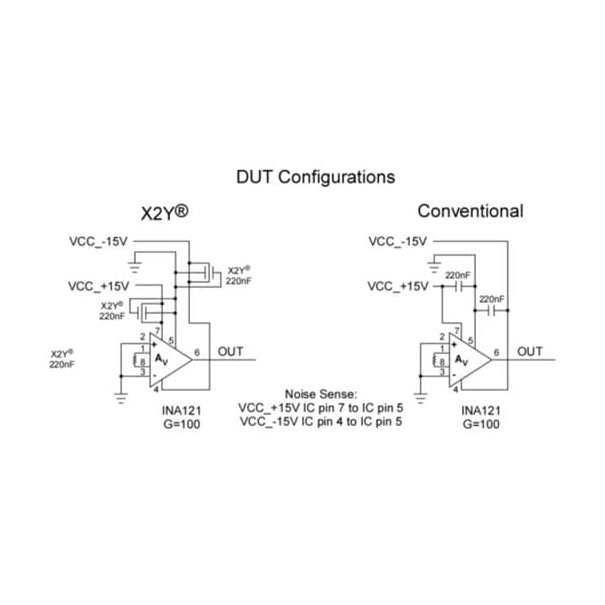
One of the most frequent hurdles engineers face when designing with the INA121 occurs before a PCB is even routed. PSpice and TINA-TI models of the INA121 are notorious for throwing "floating pin" errors or outputting severely distorted square waves during transient analysis.
Because the INA121 features a FET input with a microscopic 4 pA bias current, designers often mistakenly treat the inputs as ideal, infinite-impedance nodes. In a SPICE environment (and in the real world), connecting the input directly to a purely capacitive source, a floating thermocouple, or leaving it entirely disconnected will cause the simulation to fail. The tiny 4 pA bias current has nowhere to go; it charges the parasitic or input capacitance continuously until the internal amplifier stages are driven aggressively into the supply rails, resulting in a saturated, distorted output.
The Fix: You must ensure that all pins have a explicit DC return path to ground. When simulating (and when designing the physical circuit for AC-coupled or floating sources), place a high-value resistor—typically between 1 MΩ and 100 MΩ—from each input to ground. This bleeds off the bias current, stabilizes the DC operating point, and immediately resolves the floating node errors in TINA-TI.
Managing Offset Voltage and Saturation Anomalies
Beyond simulation, physical prototypes utilizing the INA121 can exhibit unexpected behaviors if the nuances of the datasheet are overlooked. Two specific pain points frequently arise during bench testing:
1. Higher Than Expected Offset Voltage at Low GainEngineers often test the INA121 at a gain of 1 (unity) and are surprised to find the offset voltage exceeds the 200 µV input offset specification. This happens because the total offset voltage of an instrumentation amplifier is mathematically a combination of the input stage offset and the output stage offset. At high gains (e.g., G=100), the input offset is amplified and completely dominates the error. However, at a gain of 1, the input offset is not multiplied, meaning the inherent offset of the output stage becomes a highly significant percentage of the total error. To fix this, you must calculate the total worst-case offset using the specific two-part formula provided in the manufacturer's datasheet, accounting for both $V_{OSI}$ and $V_{OSO}$.
2. Low Frequency OscillationUsers occasionally report low-frequency oscillation when the INA121 is driven into saturation against its supply rails. To mitigate this, strictly avoid driving the amplifier into deep saturation during normal operation by properly scaling your gain resistor ($R_G$). Furthermore, this oscillation is often exacerbated by poor power supply impedance. Ensure robust supply bypassing by placing a 0.1 µF ceramic capacitor directly at the supply pins, backed by a larger 10 µF tantalum or electrolytic bulk capacitor. Finally, verify that the reference pin (REF) is driven by a stable, low-impedance source (like an op-amp buffer), as any instability on the REF pin will couple directly into the output.
High-Impedance Sensor Applications in Practice
The unique specifications of the INA121 dictate its use in specific, demanding environments:
Medical Instrumentation (EMG/EKG): Human skin presents a highly variable, high-impedance interface. The 4 pA bias current prevents the amplifier from polarizing the electrodes, ensuring stable baseline readings for electrocardiograms and electromyography.
High-Impedance Sensor Interfaces: Devices like photodiode arrays, ion-selective electrodes (pH probes), and capacitive sensors require the ultra-low current noise of a FET front-end.
Strain Gauge and Load Cell Amplifiers: While bipolar amps are more common here, the INA121's low 450 µA quiescent current makes it an attractive choice for remote, battery-operated bridge measurements.
Industrial Process Control and Data Acquisition Systems: The wide 4.5V to 36V supply range allows the INA121 to interface seamlessly with standard 24V industrial control loops.
Footprint, Pinout, and Datasheet Verification
Before releasing a BOM, verify the exact package suffix and pinout. Instrumentation amplifiers generally follow an industry-standard 8-pin layout, but assumptions can lead to costly PCB respins.
Gain Setting (Pins 1 and 8): The external gain resistor ($R_G$) connects across these pins. Because the capacitance at these nodes can degrade the High Common-Mode Rejection Ratio (CMRR), PCB traces to $R_G$ must be kept as short and symmetrical as possible.
Reference Pin (Pin 5): The REF pin is used to level-shift the output voltage. A common layout mistake is connecting this pin through a high-value resistor divider. The REF pin must see a low impedance (ideally < 1 ohm); otherwise, the CMRR of the entire amplifier will be catastrophically degraded. Always buffer a resistor divider with an operational amplifier before driving the REF pin.
Package Codes: Verify the specific package codes in the latest datasheet, as thermal derating characteristics differ significantly between standard DIP packages and surface-mount SOIC variations.
Evaluating Alternatives and Replacement Options
Supply chain volatility and BOM cost optimization frequently force engineers to cross-reference components. When considering alternatives to the INA121, you must be extremely careful regarding the input architecture.
Analog Devices AD620: Often considered the industry standard instrumentation amplifier, the AD620 is frequently suggested as a drop-in replacement due to pin compatibility. Warning: The AD620 is a bipolar device. Its input bias current is in the nanoamp range, orders of magnitude higher than the INA121. If your circuit relies on the INA121's 4 pA FET input for a high-impedance sensor, swapping in an AD620 will completely break the measurement.
Texas Instruments INA128: Similar to the AD620, the INA128 is a precision bipolar amplifier. It offers lower voltage noise than the INA121 but suffers from higher current noise. It is an excellent upgrade only if the source impedance is low.
Texas Instruments INA116: If 4 pA is still too much bias current, the INA116 offers ultra-low femtoampere bias currents. However, it requires specialized guarding layouts and is not a direct footprint replacement.
Texas Instruments INA819 / INA826: These represent the modern generation of TI instrumentation amplifiers. The INA826 is a fantastic, low-cost, low-power alternative that runs on very wide supply ranges. However, like the others, verify that your source impedance can tolerate the bias current of these newer architectures before designing out the INA121.
Frequently Asked Questions
Can I replace the INA121 directly with an AD620 without changing the PCB footprint?While the 8-pin footprint and basic pinout are generally functionally compatible, they are not electrically interchangeable in all applications. The AD620 uses a bipolar input stage with significantly higher input bias current. If your design interfaces with a high-impedance source (like a pH sensor), the AD620 will introduce massive offset errors compared to the FET-input INA121.
Why is the offset voltage of my INA121 circuit much higher than 200 µV when configured as a simple buffer (Gain = 1)?At a gain of 1, the output stage offset voltage is not divided down relative to the signal, making it a major contributor to the total error. The 200 µV figure is the input offset voltage; you must calculate the total offset by adding the input offset to the output offset (as defined in the datasheet equations) to find the true expected error at low gains.
How do I minimize noise when routing the gain-setting resistor ($R_G$) for the INA121?Keep the PCB traces between the $R_G$ resistor and pins 1 and 8 as short and symmetrical as possible. Any parasitic capacitance mismatch on these pins will directly degrade the Common-Mode Rejection Ratio (CMRR) of the amplifier, allowing environmental noise to enter the signal path.
Why does my INA121 circuit show a distorted square wave in TINA-TI simulations?This is a classic "floating pin" error. FET-input amplifiers draw very little current, but they still require a DC return path to ground. If you are simulating with an ideal AC source or a floating sensor, add a high-value resistor (e.g., 10 MΩ) from the INA121 inputs to ground to provide a path for the 4 pA bias current.
Watch Tutorial: INA121
Specifications
Datasheet PDF
- Datasheets :
 CSR8675 Premium Single-Chip : Datasheet, Features and Specifications
28 July 202110296
 STM32MP157CAA3 Development: From Setup and Configuration to Advanced Features Implementation
07 June 20251428
 Exploring the STM32F103x8 and STM32F103xB Series Microcontrollers by STMicroelectronics
29 February 20241962
 TC4420 MOSFET Driver: Datasheet, Pinout, Application Circuit
13 December 202118050
 LM5122 Boost Controller: Application, Datasheet, Circuit
08 April 20225184
 P82B96 Bipolar IC: Pinout, 3D Model and Datasheet
02 November 20212945
 Upgrade Your DIY EV Build with SPC5 (MPC5xxx Automotive Series): Pro-Grade Safety Made Accessible
23 March 2026512
 AD9508 1.65 GHz Clock Buffer: Datasheet, Ultra-Low Jitter Specs, and Configuration Analysis
21 April 2026364
 Application Specific Trade-offs for WBG SIC, GaN and High End SI Power Switch Technologies
22 November 20221641
 Millimeter Wave Radar: Advantages, Types, and Applications
18 October 202120398
 How Does the A4988 Stepper Motor Driver Work
29 August 20266637
 Aluminum Electrolytic Capacitor Basis: Definition, Characteristics and Life
03 March 20226755
 Automatic Voltage Regulator: Ultimate Guide to Stable Power and Equipment Protection
06 May 202510579
 800G Optical Transceivers: The Guide for AI Data Centers
21 August 202614373
 What is a Power Capacitor?
20 November 20216565
 Beginners Guide to FPGA Design
29 December 20211263
Texas Instruments
In Stock
United States
China
Canada
Japan
Russia
Germany
United Kingdom
Singapore
Italy
Hong Kong(China)
Taiwan(China)
France
Korea
Mexico
Netherlands
Malaysia
Austria
Spain
Switzerland
Poland
Thailand
Vietnam
India
United Arab Emirates
Afghanistan
Åland Islands
Albania
Algeria
American Samoa
Andorra
Angola
Anguilla
Antigua & Barbuda
Argentina
Armenia
Aruba
Australia
Azerbaijan
Bahamas
Bahrain
Bangladesh
Barbados
Belarus
Belgium
Belize
Benin
Bermuda
Bhutan
Bolivia
Bonaire, Sint Eustatius and Saba
Bosnia & Herzegovina
Botswana
Brazil
British Indian Ocean Territory
British Virgin Islands
Brunei
Bulgaria
Burkina Faso
Burundi
Cabo Verde
Cambodia
Cameroon
Cayman Islands
Central African Republic
Chad
Chile
Christmas Island
Cocos (Keeling) Islands
Colombia
Comoros
Congo
Congo (DRC)
Cook Islands
Costa Rica
Côte d’Ivoire
Croatia
Cuba
Curaçao
Cyprus
Czechia
Denmark
Djibouti
Dominica
Dominican Republic
Ecuador
Egypt
El Salvador
Equatorial Guinea
Eritrea
Estonia
Eswatini
Ethiopia
Falkland Islands
Faroe Islands
Fiji
Finland
French Guiana
French Polynesia
Gabon
Gambia
Georgia
Ghana
Gibraltar
Greece
Greenland
Grenada
Guadeloupe
Guam
Guatemala
Guernsey
Guinea
Guinea-Bissau
Guyana
Haiti
Honduras
Hungary
Iceland
Indonesia
Iran
Iraq
Ireland
Isle of Man
Israel
Jamaica
Jersey
Jordan
Kazakhstan
Kenya
Kiribati
Kosovo
Kuwait
Kyrgyzstan
Laos
Latvia
Lebanon
Lesotho
Liberia
Libya
Liechtenstein
Lithuania
Luxembourg
Macao(China)
Madagascar
Malawi
Maldives
Mali
Malta
Marshall Islands
Martinique
Mauritania
Mauritius
Mayotte
Micronesia
Moldova
Monaco
Mongolia
Montenegro
Montserrat
Morocco
Mozambique
Myanmar
Namibia
Nauru
Nepal
New Caledonia
New Zealand
Nicaragua
Niger
Nigeria
Niue
Norfolk Island
North Korea
North Macedonia
Northern Mariana Islands
Norway
Oman
Pakistan
Palau
Palestinian Authority
Panama
Papua New Guinea
Paraguay
Peru
Philippines
Pitcairn Islands
Portugal
Puerto Rico
Qatar
Réunion
Romania
Rwanda
Samoa
San Marino
São Tomé & Príncipe
Saudi Arabia
Senegal
Serbia
Seychelles
Sierra Leone
Sint Maarten
Slovakia
Slovenia
Solomon Islands
Somalia
South Africa
South Sudan
Sri Lanka
St Helena, Ascension, Tristan da Cunha
St. Barthélemy
St. Kitts & Nevis
St. Lucia
St. Martin
St. Pierre & Miquelon
St. Vincent & Grenadines
Sudan
Suriname
Svalbard & Jan Mayen
Sweden
Syria
Tajikistan
Tanzania
Timor-Leste
Togo
Tokelau
Tonga
Trinidad & Tobago
Tunisia
Turkey
Turkmenistan
Turks & Caicos Islands
Tuvalu
U.S. Outlying Islands
U.S. Virgin Islands
Uganda
Ukraine
Uruguay
Uzbekistan
Vanuatu
Vatican City
Venezuela
Wallis & Futuna
Yemen
Zambia
Zimbabwe
![LMV722MX]() LMV722MX
LMV722MXTexas Instruments
![LMC6082AIN]() LMC6082AIN
LMC6082AINTexas Instruments
![RC4558P]() RC4558P
RC4558PTexas Instruments
![LMC6482IMM/NOPB]() LMC6482IMM/NOPB
LMC6482IMM/NOPBTexas Instruments
![LM324MX/NOPB]() LM324MX/NOPB
LM324MX/NOPBTexas Instruments
![LM324AM/NOPB]() LM324AM/NOPB
LM324AM/NOPBTexas Instruments
![LMV324IDR]() LMV324IDR
LMV324IDRTexas Instruments
![LMC7101BIM5/NOPB]() LMC7101BIM5/NOPB
LMC7101BIM5/NOPBTexas Instruments
![TLV2372IDR]() TLV2372IDR
TLV2372IDRTexas Instruments
![NE5532P]() NE5532P
NE5532PTexas Instruments


