
 Product
 Brand
Brand Articles
 Tools
Tools
AD9508 1.65 GHz Clock Buffer: Datasheet, Ultra-Low Jitter Specs, and Configuration Analysis


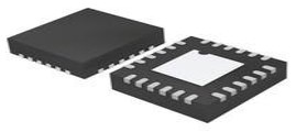
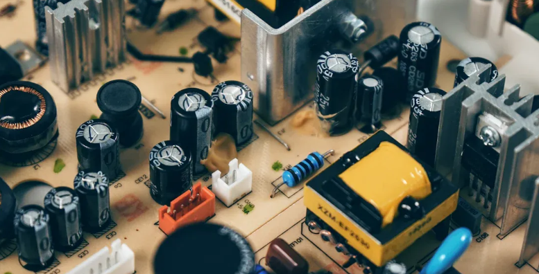
1 Circuit 2.5V 1:4 Clock Buffer QUAD AD9508 24 Pins 24-WFQFN Exposed Pad, CSP
Discover the AD9508 1.65 GHz clock fanout buffer by Analog Devices. Explore its ultra-low 41fs jitter specs, pinout, and design tips. Optimize your BOM today!
- Executive Summary: What is the AD9508?
- 1. Technical Specifications & Performance Analysis
- 2. Pinout, Package, and Configuration
- 3. Design & Integration Guide (For Engineers & Makers)
- 4. Typical Applications & Use Cases
- 5. Alternatives and Cross-Reference Guide
- 6. Frequently Asked Questions (FAQ)
- 7. Resources
- Specifications
- Parts with Similar Specs
- Datasheet PDF
Executive Summary: What is the AD9508?
The AD9508 is a 1.65 GHz clock fanout buffer designed by Analog Devices to provide highly precise clock distribution capabilities with an emphasis on ultra-low jitter for maximizing system performance. By featuring four independent differential clock outputs with programmable dividers and delay adjustment, it allows hardware engineers to synchronize complex high-speed data converter arrays and transceivers seamlessly.
Market Position: High-performance, precision timing solution geared toward low-noise applications where signal integrity is paramount.
Top Features:
1.65 GHz maximum frequency for differential inputs/outputs.
Ultra-low additive output jitter of 41 fs rms typical (12 kHz to 20 MHz).
10-bit programmable dividers (1 to 1024, all integers) with pin strapping capability.
Primary Audience: Ideal for RF designers, instrumentation engineers, and defense contractors building high-speed ADCs, DACs, and broadband infrastructure.
Supply Status: Active (Includes an "EP" version certified for defense and aerospace AQEC standards).
1. Technical Specifications & Performance Analysis
1.1 Core Architecture (CPU/Logic/Power)
The core architecture of the AD9508 revolves around its highly configurable clock distribution network. Unlike basic splitters, this buffer integrates 10-bit programmable dividers on each of its four independent channels, allowing division ratios from 1 to 1024. This architectural choice gives designers the flexibility to generate multiple synchronized clock frequencies from a single master oscillator. Furthermore, the device supports "pin strapping" for hardwired programming at power-up, eliminating the strict necessity for an external microcontroller in fixed-frequency applications.
1.2 Key Electrical Characteristics
Power and thermal management are critical when dealing with sub-picosecond jitter requirements. - Operating Supply Voltage: 2.5V or 3.3V (Single supply operation simplifies BOM and power plane design). - Maximum Frequency: 1.65 GHz. - Additive Output Jitter: 41 fs rms typical (12 kHz to 20 MHz). Broadband random jitter is kept remarkably low at <115 fs rms. - Operating Temperature Range: Standard grade operates from -40°C to +85°C, while the Enhanced Product (EP) version handles extreme environments from -55°C to +105°C.
1.3 Interfaces and Connectivity
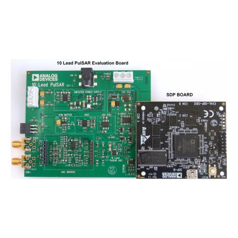
The AD9508 provides highly versatile I/O connectivity to interface with various logic families. It supports 3 programmable output logic levels: LVDS, HSTL, and 1.8V CMOS. The device can be configured to output up to 4 differential signals or 8 single-ended CMOS outputs. Configuration and communication (typically evaluated via the EVAL-AD9508 board) are handled via standard serial interfaces like I2C or SPI, allowing real-time adjustment of phase delays and divider values.
2. Pinout, Package, and Configuration
2.1 Pin Configuration Guide
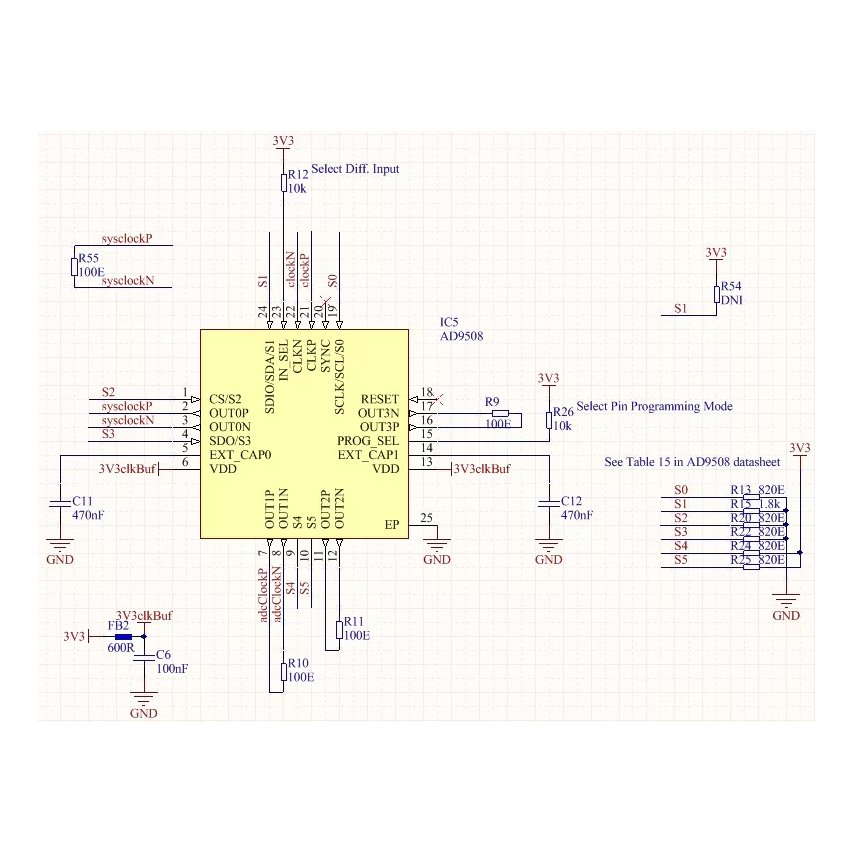
While you should always refer to the AD9508 datasheet for the exact pin layout, the pins are functionally grouped as follows: - Power & Ground (VDD, GND): Critical for maintaining low phase noise. Requires heavy decoupling. - Clock Inputs (CLK, CLK/): Differential input pairs accepting the master oscillator signal. - Clock Outputs (OUT0 to OUT3): Four independent differential pairs (can be configured as 8 CMOS). - Control Pins (PROG_SEL, SYNCb): Used for hardware state selection, pin strapping, and synchronizing the output dividers. - Serial Interface (SDIO, SCLK, CSb): Used for I2C/SPI programming.
2.2 Naming Convention & Ordering Codes
Understanding the Part Numbers:Procurement managers should pay close attention to the suffixes when evaluating price vs performance. Standard commercial/industrial variants cover the -40°C to +85°C range. The AD9508-EP suffix denotes the Enhanced Product version, which is AQEC standard compliant for defense and aerospace applications, supporting a wider -55°C to +105°C range.
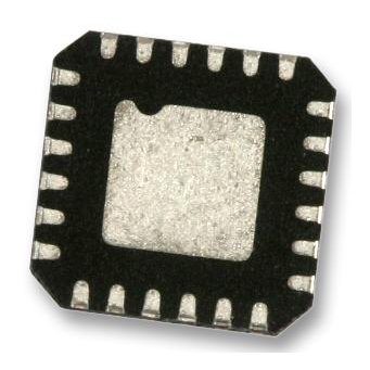
2.3 Available Packages
| Package Type | Dimensions | Common Use Case |
|---|---|---|
| LFCSP (Refer to Datasheet) | Compact footprint | High-density RF and instrumentation boards |
| EVAL Board | N/A | Prototyping and initial configuration testing |
(Note: High-frequency LFCSP packages require precise machine assembly and a robust thermal ground pad; they are not typically hand-soldering friendly.)
3. Design & Integration Guide (For Engineers & Makers)
Pro Tip: Always verify pin compatibility and logic-level termination requirements before migrating from older series like the AD9514.
3.1 Hardware Implementation
Bypass Capacitors: Place low-ESR ceramic capacitors (e.g., 0.1µF and 0.01µF) as close to the VDD pins as physically possible to suppress high-frequency power supply noise.
PCB Layout: Use continuous ground planes. Route differential clock traces closely coupled and perfectly length-matched to prevent skew. Avoid 90-degree trace bends.
Thermal Management: The exposed pad on the bottom of the package MUST be soldered to the PCB ground plane for both thermal relief and optimal electrical grounding.
3.2 Common Design Challenges
Issue: LVDS outputs show a nearly DC signal with small steps instead of a proper clock.
Fix: This is often a configuration or input termination issue. Adjust the pull-up resistor at the
PROG_SELpin, ensure proper 100-ohm differential input termination, or momentarily ground theSYNCbpin to force a reset of the internal state machine.Issue: Unable to write/read values to the EVAL-AD9508 via USB/I2C (dividers stuck at /256).
Fix: Verify that the board jumper settings match the default configuration. Ensure header P101 is set to I2C mode, and check the "Enable SDO" option within the software Control Menu.
Issue: Datasheet HSTL Specification Confusion (Current and Voltage Swings).
Fix: Note that the 11mA boost setting mentioned in the datasheet applies to LVPECL, not HSTL. Additionally, when reading Figures 20 and 21 in the datasheet, the vertical axis should be interpreted as Voltage peak-to-peak (V p-p), which is approximately 1.85V p-p.
4. Typical Applications & Use Cases
4.1 Real-World Example: Broadband Infrastructure & High-Speed ADCs
In broadband infrastructure, such as 5G base stations, baseband processors must sample incoming analog signals with extreme precision. Even a few picoseconds of clock jitter can degrade the Signal-to-Noise Ratio (SNR) of a high-speed Analog-to-Digital Converter (ADC) or Mixed-Signal Front End (MxFE).
The AD9508 fits into this product by taking a highly stable reference clock (like an OCXO), dividing it down if necessary, and fanning it out to multiple ADCs and DACs simultaneously. Its 41 fs additive jitter ensures that the clock distribution network does not bottleneck the RF performance, while the programmable delay allows engineers to fine-tune the phase alignment between multiple data converters.
5. Alternatives and Cross-Reference Guide
When balancing BOM costs, availability, and specs, you may need to look at alternatives. The AD9508 competes directly in the ultra-low jitter fanout buffer market.
Direct Replacements / Competitors:
LTC6954: Offers excellent low phase noise and similar divider capabilities, often used in similar RF clocking applications.
HMC7043: A high-performance clock distributor from Analog Devices (formerly Hittite) that supports up to 14 outputs, ideal if you need more channels than the AD9508's four outputs.
Better Performance / Upgrades:
ADCLK948: Consider this if you need ultra-high-speed routing without the complex divider networks, offering sub-100 fs jitter for pure ECL/PECL logic.
Legacy Equivalents:
AD9514: An older clock distribution IC. The AD9508 is generally a superior upgrade choice due to better jitter performance and more flexible divider logic.
6. Frequently Asked Questions (FAQ)
Q: What is the difference between AD9508 and the legacy AD9514? A: The AD9508 provides significantly better additive jitter performance (41 fs rms) and more flexible 10-bit programmable dividers (1 to 1024) compared to the older AD9514, making it better suited for modern high-speed ADCs and DACs.
Q: Can AD9508 be used in defense and aerospace applications? A: Yes, the AD9508-EP version is specifically certified to the AQEC standard and supports an extended operating temperature range of -55°C to +105°C.
Q: Where can I find the datasheet and library files for AD9508? A: The official AD9508 datasheet, evaluation software, and CAD/schematic symbols can be downloaded directly from the Analog Devices website or authorized distributors.
Q: Is AD9508 suitable for battery-operated devices? A: While it operates on a relatively low 2.5V/3.3V supply, it is designed for high-performance infrastructure rather than ultra-low-power battery devices. It consumes more power than standard micro-power oscillators due to its high-speed 1.65 GHz capability.
Q: How do I program/configure the AD9508? A: It can be hardwired at power-up using pin strapping for fixed configurations, or programmed dynamically via its serial interface (I2C/SPI) using a microcontroller or the EVAL-AD9508 evaluation board.
7. Resources
Development Tools & Software:
EVAL-AD9508: The official evaluation board for testing I2C/SPI communications, divider setups, and measuring phase noise.
Analog Devices Clock Design Tool: Software available from ADI to help simulate clock trees and calculate expected system jitter.
Specifications
Parts with Similar Specs
- ImagePart NumberManufacturerPackage / CaseNumber of PinsNumber of CircuitsFrequency (Max)Supply VoltageTerminal PitchFactory Lead TimeMoisture Sensitivity Level (MSL)View Compare
![AD9508BCPZ-REEL7]()
AD9508BCPZ-REEL7
24-WFQFN Exposed Pad, CSP
24
1
1.65GHz
2.5 V
0.5 mm
8 Weeks
3 (168 Hours)
![ADCLK946BCPZ]()
24-VFQFN Exposed Pad, CSP
24
1
-
3.3 V
0.5 mm
8 Weeks
3 (168 Hours)
![ADCLK846BCPZ-REEL7]()
24-VFQFN Exposed Pad, CSP
24
1
4.8GHz
3.3 V
0.5 mm
8 Weeks
3 (168 Hours)
![ADCLK846BCPZ]()
24-VFQFN Exposed Pad, CSP
24
1
-
1.8 V
0.5 mm
8 Weeks
3 (168 Hours)
![ADCLK946BCPZ-REEL7]()
24-VFQFN Exposed Pad, CSP
24
1
1.2GHz
1.8 V
0.5 mm
8 Weeks
3 (168 Hours)


Datasheet PDF
- Datasheets :
- PCN Assembly/Origin :
- PCN Design/Specification :
- ConflictMineralStatement :
 APX803S 3-Pin Microprocessor Reset Circuit: Pinout, Equivalent and Datasheet
02 March 20221732
 ADG1414 SPST Switches: Pinout, Features and Datasheet
15 February 20222875
 TLC274 Quad Op-Amp Design Notes: Overcoming Single-Supply Swing Limitations
03 June 202696
 STM8L151C4U6 Microcontroller: Technical Overview
29 February 2024145
 SN74LVC2G17DCKR Dual Schmitt-Trigger Buffer: Circuit, Pinout, and Datasheet
29 March 20223430
 LM5002MAX/NOPB: Pinout, High-Voltage, CAD Model
21 February 2022970
 SP2502LBTG TVS Diode: Pinout, Datasheet, Schematic
30 August 2021543
 A Comprehensive Guide to the 5962-8770203RX Digital to Analog Converter (DAC)
06 March 2024166
 Basic Introduction to the Types of Capacitors
16 October 202510501
 How to Properly Install TVS Diodes in Your PCB Design
11 July 20254977
 Introduction to Semiconductor Devices
17 October 202515310
 Ohmic Resistors: Differences, Laws, and Applications
08 June 202613890
 What is Digital Power Supply?
10 November 20203372
 How Top Wire Splice Connector Brands Stack Up This Year
10 July 20252644
 How to Distinguish MOSFET? Is it N-Channel or P-Channel?
23 December 202111234
 Characteristics and Working Principle of IGBT
31 October 202522805
Analog Devices Inc.
In Stock: 51
United States
China
Canada
Japan
Russia
Germany
United Kingdom
Singapore
Italy
Hong Kong(China)
Taiwan(China)
France
Korea
Mexico
Netherlands
Malaysia
Austria
Spain
Switzerland
Poland
Thailand
Vietnam
India
United Arab Emirates
Afghanistan
Åland Islands
Albania
Algeria
American Samoa
Andorra
Angola
Anguilla
Antigua & Barbuda
Argentina
Armenia
Aruba
Australia
Azerbaijan
Bahamas
Bahrain
Bangladesh
Barbados
Belarus
Belgium
Belize
Benin
Bermuda
Bhutan
Bolivia
Bonaire, Sint Eustatius and Saba
Bosnia & Herzegovina
Botswana
Brazil
British Indian Ocean Territory
British Virgin Islands
Brunei
Bulgaria
Burkina Faso
Burundi
Cabo Verde
Cambodia
Cameroon
Cayman Islands
Central African Republic
Chad
Chile
Christmas Island
Cocos (Keeling) Islands
Colombia
Comoros
Congo
Congo (DRC)
Cook Islands
Costa Rica
Côte d’Ivoire
Croatia
Cuba
Curaçao
Cyprus
Czechia
Denmark
Djibouti
Dominica
Dominican Republic
Ecuador
Egypt
El Salvador
Equatorial Guinea
Eritrea
Estonia
Eswatini
Ethiopia
Falkland Islands
Faroe Islands
Fiji
Finland
French Guiana
French Polynesia
Gabon
Gambia
Georgia
Ghana
Gibraltar
Greece
Greenland
Grenada
Guadeloupe
Guam
Guatemala
Guernsey
Guinea
Guinea-Bissau
Guyana
Haiti
Honduras
Hungary
Iceland
Indonesia
Iran
Iraq
Ireland
Isle of Man
Israel
Jamaica
Jersey
Jordan
Kazakhstan
Kenya
Kiribati
Kosovo
Kuwait
Kyrgyzstan
Laos
Latvia
Lebanon
Lesotho
Liberia
Libya
Liechtenstein
Lithuania
Luxembourg
Macao(China)
Madagascar
Malawi
Maldives
Mali
Malta
Marshall Islands
Martinique
Mauritania
Mauritius
Mayotte
Micronesia
Moldova
Monaco
Mongolia
Montenegro
Montserrat
Morocco
Mozambique
Myanmar
Namibia
Nauru
Nepal
New Caledonia
New Zealand
Nicaragua
Niger
Nigeria
Niue
Norfolk Island
North Korea
North Macedonia
Northern Mariana Islands
Norway
Oman
Pakistan
Palau
Palestinian Authority
Panama
Papua New Guinea
Paraguay
Peru
Philippines
Pitcairn Islands
Portugal
Puerto Rico
Qatar
Réunion
Romania
Rwanda
Samoa
San Marino
São Tomé & Príncipe
Saudi Arabia
Senegal
Serbia
Seychelles
Sierra Leone
Sint Maarten
Slovakia
Slovenia
Solomon Islands
Somalia
South Africa
South Sudan
Sri Lanka
St Helena, Ascension, Tristan da Cunha
St. Barthélemy
St. Kitts & Nevis
St. Lucia
St. Martin
St. Pierre & Miquelon
St. Vincent & Grenadines
Sudan
Suriname
Svalbard & Jan Mayen
Sweden
Syria
Tajikistan
Tanzania
Timor-Leste
Togo
Tokelau
Tonga
Trinidad & Tobago
Tunisia
Turkey
Turkmenistan
Turks & Caicos Islands
Tuvalu
U.S. Outlying Islands
U.S. Virgin Islands
Uganda
Ukraine
Uruguay
Uzbekistan
Vanuatu
Vatican City
Venezuela
Wallis & Futuna
Yemen
Zambia
Zimbabwe
![AD9512BCPZ]() AD9512BCPZ
AD9512BCPZAnalog Devices Inc.
![ADCLK846BCPZ]() ADCLK846BCPZ
ADCLK846BCPZAnalog Devices Inc.
![ADCLK914BCPZ-WP]() ADCLK914BCPZ-WP
ADCLK914BCPZ-WPAnalog Devices Inc.
![ADCLK854BCPZ]() ADCLK854BCPZ
ADCLK854BCPZAnalog Devices Inc.
![ADCLK925BCPZ-WP]() ADCLK925BCPZ-WP
ADCLK925BCPZ-WPAnalog Devices Inc.
![AD9508BCPZ]() AD9508BCPZ
AD9508BCPZAnalog Devices Inc.
![LTC6957IMS-3#PBF]() LTC6957IMS-3#PBF
LTC6957IMS-3#PBFAnalog Devices, Inc.
![ADCLK914BCPZ-R2]() ADCLK914BCPZ-R2
ADCLK914BCPZ-R2Analog Devices Inc.
![AD9510BCPZ-REEL7]() AD9510BCPZ-REEL7
AD9510BCPZ-REEL7Analog Devices Inc.
![LTC6957IDD-3#PBF]() LTC6957IDD-3#PBF
LTC6957IDD-3#PBFLinear Technology/Analog Devices


