
 Product
 Brand
Brand Articles
 Tools
Tools
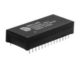
AD9253 Quad 14-Bit ADC: Integration Notes, Reset Timing, and Drop-In Alternatives

14 Bit 0.5mm Gold ADC AD9253 1.8V 48-WFQFN Exposed Pad, CSP
Unit Price: $370.866393
Ext Price: $370.87


14 Bit 0.5mm Gold ADC AD9253 1.8V 48-WFQFN Exposed Pad, CSP
Explore AD9253 design considerations, from managing 125 MSPS LVDS outputs and critical startup timing to evaluating pin-compatible drop-in replacements.
- Core Performance Metrics and Electrical Tradeoffs
- Serial LVDS Interface Considerations
- Critical Startup Sequences and Reset Timing (Firmware Warning)
- Mitigating Random Glitches and Data Purity Issues
- Target Applications for a Quad 14-Bit Architecture
- Evaluating AD9253 Alternatives and Drop-In Replacements
- Datasheet Verification and Footprint Preparation
- Specific Engineering FAQs
- Specifications
- Parts with Similar Specs
- Datasheet PDF
The AD9253 is a quad, 14-bit analog-to-digital converter (ADC) designed for high-speed data acquisition systems requiring low power consumption, compact footprints, and integrated sample-and-hold circuitry. Operating at up to 125 MSPS, this Analog Devices component is frequently selected for multi-channel systems where synchronicity and thermal efficiency are critical.
When integrating a high-speed quad ADC, engineers must balance signal fidelity against the complexities of routing multiple high-speed digital buses. The component’s architecture simplifies some of this by utilizing serial LVDS outputs, but it introduces specific initialization and timing constraints that firmware and hardware teams must handle carefully.
Primary Market Position: Mid-to-high-speed, high-resolution multi-channel data acquisition.
Key Selection Factor: The balance of 14-bit resolution at 125 MSPS while consuming only 110 mW per channel.
Major Design Hurdle: Strict clock stability requirements during startup and highly specific SPI reset wait times.
Core Performance Metrics and Electrical Tradeoffs
Evaluating the AD9253 requires looking past the top-line sample rate and understanding the dynamic performance compromises inherent in low-power 1.8 V designs.
The ADC delivers a Signal-to-Noise Ratio (SNR) of 74 dB and a Spurious-Free Dynamic Range (SFDR) of 90 dBc (both to Nyquist). For a 14-bit converter operating at 125 MSPS, these are strong figures that provide excellent headroom for undersampling applications. The full power analog bandwidth extends to 650 MHz, allowing the device to capture high-frequency intermediate frequency (IF) signals well beyond the first Nyquist zone.
However, achieving this performance requires extremely clean power. The 1.8 V supply operation is excellent for minimizing overall system power consumption—totaling roughly 440 mW across all four channels at full speed—but a 1.8 V rail is highly susceptible to noise. Any ripple or switching noise on the analog supply will directly degrade the SFDR and introduce unwanted spurs.
Linearity: Typical Differential Non-Linearity (DNL) is ±0.75 LSB, and Integral Non-Linearity (INL) is ±2.0 LSB. This ensures excellent tonal purity, provided the front-end drive circuitry can cleanly deliver the required 2 V p-p input voltage range.
Power Down: The device includes both full-chip and individual channel power-down modes. This is highly useful in scalable systems (like portable ultrasound) where channels can be disabled to conserve battery life when not actively imaging.
Serial LVDS Interface Considerations
To manage the massive data payload of four 14-bit channels running at 125 MSPS, the AD9253 utilizes a serial LVDS (ANSI-644 default) output format. This reduces the pin count drastically compared to parallel CMOS outputs, enabling a much smaller package size.
The engineering cost of this interface is the requirement for precise impedance matching and length tuning on the PCB. The LVDS lanes must be routed as 100-ohm differential pairs. The device also offers a low-power, reduced-signal LVDS option, which can save power and reduce electromagnetic interference (EMI) if the receiving FPGA or ASIC is physically close to the ADC and can reliably detect smaller voltage swings.
Critical Startup Sequences and Reset Timing (Firmware Warning)
One of the most complex aspects of integrating the AD9253 lies in its initialization and reset behavior. Misunderstanding these sequences leads to some of the most common—and frustrating—system failures observed by design teams.
Preventing Distorted Samples on Power-Up
A rare but documented issue occurs where one channel will output heavily distorted data accompanied by high harmonics immediately upon startup. This is almost always a hardware sequencing fault rather than a defective chip. To fix or prevent this, the clock input must be completely stable before the ADC turns on. If the clock is drifting, settling, or experiencing glitches while the AD9253 is executing its internal power-on reset, the internal state machine can lock into an invalid state. Strict adherence to the initialization procedure, ensuring the clock synthesizer or oscillator is fully locked before bringing the ADC out of power-down, is mandatory.
Managing the 2.9 Million Clock Cycle Reset Penalty
If the system issues a soft reset or a digital reset via the SPI bus, the outputs will not immediately return to a usable state. Outputs will often appear inconsistent or completely non-functional right after the command is sent.
The fix for this requires a massive, non-intuitive wait state in the firmware. After issuing a reset, the system must wait for 2.9 million sample clocks before resuming normal operation. At lower sample rates, this translates to a significant real-time delay. For example, if the ADC is being clocked at 16.82 MHz, 2.9 million clocks equals approximately 172 milliseconds. Firmware engineers must account for this delay to prevent the FPGA or microcontroller from ingesting garbage data or triggering false system faults during a warm reboot.
Mitigating Random Glitches and Data Purity Issues
Even after successful initialization, engineers occasionally encounter random glitches or noise spikes in the ADC data that appear completely independent of the actual analog input signal. When this happens, it usually indicates a misalignment in the digital interface timing or a corrupted internal digital state.
If data purity is suddenly compromised by random bit errors:
Issue a Digital Reset: Write to Register 0x08. The exact sequence must be
0x00->0x03->0x00.Verify Interface Timing: Re-check the digital interface timing and bit alignments between the ADC's data clock output (DCO), frame clock output (FCO), and the receiving FPGA's input delay elements (IDELAY). Changes in die temperature can sometimes shift these timings enough to cause setup/hold violations at high speeds, manifesting as "random glitches."
Target Applications for a Quad 14-Bit Architecture
The combination of four phase-aligned channels, high analog bandwidth, and low power makes the AD9253 highly targeted toward specific industries.
Medical Ultrasound: Phased array ultrasound systems require dozens or hundreds of synchronous ADC channels. The low power (110 mW/ch) prevents the transducer wand or portable base unit from overheating, while the quad-channel density keeps the PCB compact.
Quadrature and Diversity Radio Receivers: In modern SDRs (Software Defined Radios) and telecommunications equipment, capturing I and Q (In-phase and Quadrature) signals simultaneously is critical. Two AD9253s can easily handle an 8-antenna diversity receiver array.
Test Equipment: Oscilloscopes and multi-channel analyzers benefit from the built-in and custom digital test pattern generation, allowing the digital backend to verify data link integrity before analog measurements begin.
Evaluating AD9253 Alternatives and Drop-In Replacements
Supply chain volatility and evolving system requirements often force engineers to look for alternatives. Fortunately, the AD9253 exists within a family of related converters, and third-party drop-in replacements do exist.
Upgrading for Speed: Analog Devices AD9254
If your system requires a higher Nyquist boundary or faster oversampling, the AD9254 is the immediate upgrade path. It pushes the sample rate to 150 MSPS. The trade-off is higher power consumption and tighter timing margins on the LVDS interface, but the architectural similarities make firmware migration relatively painless.
Cost-Down Redesign: Analog Devices AD9633
If 14-bit resolution is over-spec'd for your final product and BOM cost needs to be reduced, the AD9633 is a 12-bit pin-compatible alternative. Because it shares the same footprint, you can seamlessly drop it onto the same PCB. The lowest two bits are simply ignored or tied off depending on the exact FPGA implementation.
Direct Sourcing Alternative: ChisynV CD14AD125Q
For procurement teams facing severe lead times or seeking second-source leverage, the ChisynV CD14AD125Q is marketed as a direct drop-in replacement for the AD9253. While pin compatibility and functional equivalence are strong, replacing an Analog Devices data converter with a third-party silicon alternative requires rigorous re-qualification. You must thoroughly test the analog bandwidth matching, thermal dissipation, and dynamic performance (SNR/SFDR) across your full operating temperature range, as the underlying silicon process differs.
Architectural Alternatives: Teledyne e2v High-Speed ADCs
If the project is moving toward space-grade or ultra-high-reliability military applications, Teledyne e2v offers competing quad-channel ADCs. These are rarely pin-compatible and will require a full board spin, but they often provide enhanced radiation tolerance and extended temperature qualifications that standard commercial AD9253 variants may not meet.
Datasheet Verification and Footprint Preparation
Before releasing a BOM or finalizing a PCB layout featuring the AD9253, several specific details must be verified against the manufacturer's documentation.
Thermal Pad Design: While 440 mW of total power is low for a quad ADC, it is still enough to cause localized heating in a dense layout. Verifying the exact mechanical dimensions and thermal pad layout in the latest manufacturer documentation is strictly required here. The exposed paddle must be soldered to a solid ground plane with multiple thermal vias to ensure the device operates within its recommended temperature profile.
Ordering Suffixes: Pay close attention to the ordering codes. Suffixes dictate the maximum speed grade (80 MSPS, 105 MSPS, or 125 MSPS), temperature range, and tape-and-reel quantities. Ordering an 80 MSPS variant for a 125 MSPS design will result in timing failures.
EDA Libraries: When importing the schematic symbol, ensure that the analog inputs (VIN+ / VIN-) are clearly separated from the LVDS digital outputs to prevent accidental cross-domain routing during the layout phase.
Specific Engineering FAQs
Why does channel one output distorted harmonics on power-up?This typically happens if the clock input is unstable while the ADC is booting. The internal state machine can lock into an invalid state. Ensure your clock source is fully locked and stable before taking the AD9253 out of its power-down or reset state.
Can I swap the AD9253 for the AD9633 without changing the PCB footprint?Yes, the AD9633 is a 12-bit pin-compatible alternative. Hardware changes are generally not required, but your FPGA firmware must be updated to expect a 12-bit payload rather than a 14-bit payload to avoid bit-shifting errors.
How long must the system wait after issuing a digital reset via SPI?The AD9253 requires a wait time of exactly 2.9 million sample clocks after a soft or digital reset before normal operation resumes. Depending on your sample rate, this can be a fraction of a second (e.g., ~23 ms at 125 MSPS) or significantly longer at lower clock speeds.
Why are there random glitches in my ADC data even when the analog input is grounded?Random glitches independent of the analog signal usually point to digital interface timing violations. Changes in temperature can shift the FCO/DCO timings relative to the data lines. Issue a digital reset (Register 0x08 = 0x00 -> 0x03 -> 0x00) and verify the setup/hold margins at your FPGA IDELAY blocks.
Watch Tutorial: AD9253
Specifications
Parts with Similar Specs
- ImagePart NumberManufacturerPackage / CaseNumber of PinsNumber of BitsSampling RateInterfaceIntegral Nonlinearity (INL)Differential NonlinearityMin Supply VoltageSupply VoltageView Compare
![AD9253TCPZR7-125EP]()
AD9253TCPZR7-125EP
48-WFQFN Exposed Pad, CSP
48
14
125 Msps
LVDS, SPI, Serial
2 LSB
1.5 LSB
1.7 V
1.8 V
![AD9261BCPZRL7-10]()
48-VFQFN Exposed Pad
48
14
160 Msps
DDR, LVDS, Parallel
2 LSB
0.5 LSB
1.7 V
1.8 V
![ADS6225IRGZT]()
48-VFQFN Exposed Pad
48
12
105 Msps
LVDS, Serial
2.2 LSB
-
3 V
3.3 V
![ADS4146IRGZT]()
48-VFQFN Exposed Pad
48
12
125 Msps
LVDS, Serial
2.5 LSB
-
3 V
3.3 V
![ADS6224IRGZT]()
48-VFQFN Exposed Pad, CSP
48
16
160 Msps
Parallel, SPI, Serial
1.5 LSB
-
1.7 V
1.8 V


Datasheet PDF
- Datasheets :
- ConflictMineralStatement :
 Designing Ultra-Compact Electronics with ATTINY10: Specs, Pinout, and TPI Programming
06 February 2026195
![Understanding of TP5100 2A Lithium Battery Charger Module [FAQ]](https://res.utmel.com/Images/Article/418b1a45-e558-4b3e-9fc7-c3c70e1c638a.jpg) Understanding of TP5100 2A Lithium Battery Charger Module [FAQ]
Understanding of TP5100 2A Lithium Battery Charger Module [FAQ]12 April 202217924
 ES110-0017 Sensor: Datasheet, Application, Features
01 September 2021911
![LM741 Op Amp: Datasheet, Pinout, Applications, Equivalent , LM741 vs LM358[FAQ+Video]](https://res.utmel.com/Images/Article/982185fd-9ad4-49d4-a815-4b79ef0651a6.jpg) LM741 Op Amp: Datasheet, Pinout, Applications, Equivalent , LM741 vs LM358[FAQ+Video]
LM741 Op Amp: Datasheet, Pinout, Applications, Equivalent , LM741 vs LM358[FAQ+Video]18 April 202222203
 Introduction to Microchip PIC24EP64GP204
29 February 2024110
 DS1693 RTC: Datasheet, Pinout, Features
31 August 2021587
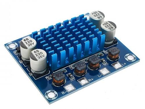 What you need to know about TPA3110 Bluetooth Audio Power Amplifier Board
26 April 202218310
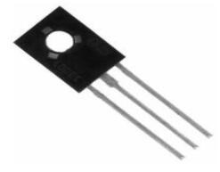 BD437 Transistor: BD437 Pinout, Datasheet, Equivalent
06 April 20223948
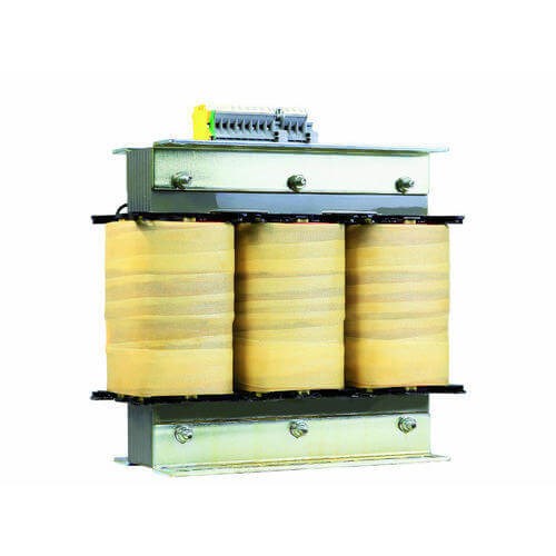 An Overview of Isolation Transformers
17 September 202014972
 Solid-state Drive (SSD): Classification and Architecture
22 May 202116971
 Electronic Components in the Smart Home System
24 April 20252861
 Buffer Amplifier | Operating Principle, Advantages, and Applications
21 July 202510290
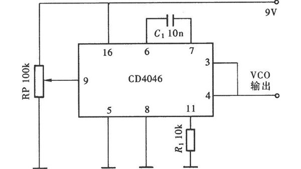 What is a Voltage Controlled Oscillator?
09 January 20269315
 Challenges in Enhancing Power Electronic Systems with Artificial Intelligence
26 December 20233119
 Electronic components distributor UTMEL Stands Out at electronica china 2024
09 July 20244820
 Understanding of Coaxial Cable
06 August 202139474
Analog Devices Inc.
In Stock: 2015
Minimum: 1 Multiples: 1
Qty
Unit Price
Ext Price
1
$370.866393
$370.87
10
$349.873956
$3,498.74
100
$330.069770
$33,006.98
500
$311.386575
$155,693.29
1000
$293.760920
$293,760.92
Not the price you want? Send RFQ Now and we'll contact you ASAP.
Inquire for More Quantity
![ADV7513BSWZ]() ADV7513BSWZ
ADV7513BSWZAnalog Devices, Inc.
![AD9877ABSZ]() AD9877ABSZ
AD9877ABSZAnalog Devices, Inc.
![LTC2245CUH#TRPBF]() LTC2245CUH#TRPBF
LTC2245CUH#TRPBFLinear Technology/Analog Devices
![AD7791BRMZ-REEL]() AD7791BRMZ-REEL
AD7791BRMZ-REELAnalog Devices Inc.
![AD7799BRUZ-REEL]() AD7799BRUZ-REEL
AD7799BRUZ-REELAnalog Devices Inc.
![AD7190BRUZ-REEL]() AD7190BRUZ-REEL
AD7190BRUZ-REELAnalog Devices Inc.
![AD7705BRZ-REEL]() AD7705BRZ-REEL
AD7705BRZ-REELAnalog Devices Inc.
![AD7175-2BRUZ-RL7]() AD7175-2BRUZ-RL7
AD7175-2BRUZ-RL7Analog Devices Inc.
![AD7192BRUZ-REEL]() AD7192BRUZ-REEL
AD7192BRUZ-REELAnalog Devices Inc.
![AD9283BRSZ-RL100]() AD9283BRSZ-RL100
AD9283BRSZ-RL100Analog Devices Inc.


