
 Product
 Brand
Brand Articles
 Tools
Tools
AD9694 Quad 14-Bit ADC Integration Notes: Resolving JESD204B Sync and Thermal Challenges

14 Bit 0.5mm ADC AD9694 0.975V 72-VFQFN Exposed Pad, CSP
Unit Price: $982.126649
Ext Price: $982.13


14 Bit 0.5mm ADC AD9694 0.975V 72-VFQFN Exposed Pad, CSP
Designing with the AD9694 quad 14-bit 500 MSPS ADC? Explore key specifications, JESD204B SYSREF synchronization fixes, thermal layout management, and alternatives.
The AD9694 is a quad, 14-bit, 500 MSPS analog-to-digital converter (ADC) designed for sampling wide bandwidth analog signals up to 1.4 GHz. Built to handle dense, high-frequency signal processing, this component is heavily utilized in multi-band digital receivers, software-defined radios, and radar systems where channel density and dynamic range are paramount.
While the integration of four high-speed ADCs into a single package drastically reduces board space, it introduces specific engineering compromises. System designers must carefully navigate high-speed serial routing, complex clock synchronization across multiple converters, and aggressive thermal management.
Core Specifications and Electrical Characteristics
Understanding the baseline capabilities of this ADC is critical before committing it to a BOM or schematic. The device balances high-frequency sampling with power efficiency per channel, but the aggregate metrics dictate the surrounding power and clocking architecture.
Resolution and Speed: 14-Bit resolution at a 500 MSPS sample rate. This provides the necessary dynamic range for isolating weak signals in crowded RF environments.
Analog Input Bandwidth: 1.4 GHz full power bandwidth allows for direct RF sampling in lower frequency bands or wideband IF sampling, reducing the need for additional downconversion stages.
Power Consumption: The device draws 1.66 W total at 500 MSPS. While 415 mW per ADC channel is highly efficient for this performance class, the aggregate power in a single IC presents layout challenges.
Digital Processing: Features 4 integrated wideband digital processors with 48-bit numerically controlled oscillators (NCOs).
Operating Temperature: Rated for extreme environments from -40°C to +105°C, making it viable for ruggedized military or aerospace instrumentation.
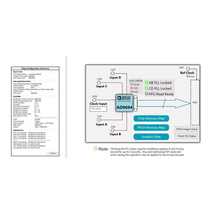
Overcoming JESD204B Link Initialization and SYSREF Synchronization Challenges
The most significant design hurdle when integrating this quad ADC is managing the JESD204B (Subclass 1) coded serial digital outputs. Operating with lane rates up to 15 Gbps, the interface minimizes pin count but dramatically increases protocol complexity.
Engineers frequently encounter Code Group Synchronization (CGS) and Initial Lane Alignment Sequence (ILAS) errors during link initialization, even when the physical clock signals appear stable on an oscilloscope. These JESD204B link errors are almost always tied to subclass 1 reference clock locking. To resolve this, you must verify all JESD204B parameters in the FPGA or ASIC receiver and ensure the correct reference clock (e.g., a clean 500 MHz source) is supplied, properly terminated, and fully locked before the link attempts to come up.
Furthermore, in phased-array radars or diversity receivers, maintaining phase alignment across multiple ADCs is strictly required. Users often report difficulties synchronizing the clock divider reset on SYSREF events across multiple AD9694 ICs. If SYSREF is not captured correctly by the device clock, the internal dividers will power up in unknown phase states, destroying multi-channel alignment.
To fix SYSREF synchronization issues:
Validate Setup and Hold Timings: The SYSREF signal must meet strict setup and hold times relative to the device clock. Because timing tolerances vary slightly across temperature gradients and sub-variants, confirming these threshold margins directly in the latest spec sheet is strictly required here.
Register Configuration: Verify the proper configuration of the clock divider autophase adjust.
Synchronization Mode: Ensure the synchronization mode registers are correctly set to continuous or one-shot mode depending on your system's deterministic latency requirements.
Thermal Management for the 72-Lead LFCSP
Packing four 500 MSPS ADCs into a single 72-lead LFCSP creates an extreme localized heat source. The 1.66 W total power dissipation might seem manageable on paper, but high power density in such a compact footprint will lead to thermal throttling or premature failure if the PCB layout is not optimized.
You cannot rely on the top of the plastic package for heat dissipation. The primary thermal path is through the bottom exposed pad.
Follow these thermal layout mandates:
Exposed Pad Soldering: The thermal heat slug must be soldered directly to a corresponding ground pad on the PCB.
Thermal Vias: Implement a dense array of thermal vias (typically 0.2mm to 0.3mm drill size) directly under the exposed pad to wick heat into the internal ground planes.
Copper Weight: Use 2 oz or heavier copper for the internal ground planes if the system operates near the +105°C upper temperature limit.
Derating: Exact thermal derating will depend heavily on your PCB copper area and airflow. A densely packed RF board with minimal airflow will require aggressive thermal relief design to keep the junction temperature within safe limits.
Applications in Multi-Band Receivers and Radar
The feature set of this ADC dictates its use in specialized, high-bandwidth applications. The inclusion of on-chip dithering improves small signal linearity, which is critical when detecting faint radar returns or distant communication signals. Additionally, the integrated amplitude detect bits allow for highly efficient Automatic Gain Control (AGC) implementations without requiring the FPGA to parse the full data stream first.
Primary applications include:
* Diversity Multiband Receivers: Handling 3G/4G, W-CDMA, GSM, LTE, and LTE-A signals simultaneously.
* Radars and SIGINT: Signals intelligence and ultrawideband satellite receivers benefit from the 1.4 GHz input bandwidth and quad-channel density for phase interferometry or beamforming.
* General-Purpose Software Radios (SDR): The 48-bit NCOs allow flexible digital tuning across wide spectrums.
Alternatives, Equivalents, and Replacement Considerations
If the AD9694 does not perfectly align with your BOM constraints, cost targets, or availability requirements, Analog Devices offers several related converters. However, be aware that moving between these parts often requires schematic updates, as they are not all drop-in replacements.
AD9690 & AD9680: The AD9680 is a dual-channel 14-bit ADC, while the AD9690 is a single-channel version. These are excellent fallbacks if your channel density requirements drop and you want to save power or simplify the JESD204B routing.
AD9234: A dual 12-bit, 1 GSPS ADC. Consider this if you need higher sample rates but can sacrifice resolution and two channels.
AD9695 & AD9697: These belong to similar high-speed data converter families. The AD9695 is a dual 14-bit 1300 MSPS ADC. Upgrading to these parts will require a complete re-evaluation of your clocking architecture and JESD204B lane rates due to the massive increase in data throughput.
When evaluating any of these alternatives, cross-reference the exact package codes and JESD204B subclass requirements, as second-sourcing high-speed converters usually triggers a full requalification of the DSP firmware.
Schematic, Pinout, and Layout Verification
Before finalizing your PCB layout, verify the 72-lead LFCSP footprint against the manufacturer's mechanical drawings. Pay special attention to:
* Analog vs. Digital Ground Separation: While modern high-speed ADCs often recommend a single solid ground plane under the IC, verify the specific return current paths for the 15 Gbps JESD204B lanes to prevent digital noise from coupling into the 1.4 GHz analog front end.
* Lane Routing: Keep the serial digital output lanes matched in length and routed as 100-ohm differential pairs.
* Power Supply Decoupling: Place high-frequency decoupling capacitors (e.g., 0402 or 0201 packages) on the same side of the board as the ADC, as close to the power pins as physically possible to minimize parasitic inductance.
Frequently Asked Questions
Why am I seeing CGS and ILAS errors when bringing up the AD9694 JESD204B link?
These errors typically occur when the Subclass 1 reference clock (e.g., 500 MHz) is not properly locked before initialization, or if there is a mismatch in the JESD204B parameter configuration (like the number of lanes, octets per frame, or scrambling settings) between the ADC and the receiving FPGA.
Can I replace the AD9694 with the AD9680 without changing the PCB footprint?
No. The AD9694 is a quad-channel ADC in a 72-lead LFCSP, while the AD9680 is a dual-channel ADC typically housed in a different package format (such as a 64-lead LFCSP). A footprint redesign and firmware update are required.
How do I manage the 1.66 W heat dissipation in the LFCSP package?
You must solder the exposed thermal pad on the bottom of the IC to a grounded PCB thermal slug. Use a dense grid of thermal vias to transfer the heat into the internal copper ground planes, and ensure your ambient operating conditions allow for sufficient thermal headroom below the +105°C maximum operating temperature.
Why are my multiple AD9694 ADCs powering up out of phase?
This is a SYSREF synchronization failure. If the SYSREF signal violates the setup and hold times relative to the device clock, the internal clock dividers will reset unpredictably. Verify your autophase adjust registers and ensure trace lengths for the clock and SYSREF signals are strictly matched across all ADCs in the array.
Specifications
Datasheet PDF
- Datasheets :
- Other Related Documents :
- PCN Design/Specification :
- ConflictMineralStatement :
 What do you need to know about M24M01 SMT Serial I2C bus EEPROM
07 April 20222306
![The Comprehensive Introduction to AD8310 [FAQ]](https://res.utmel.com/Images/Article/90927bcc-34e5-4a68-ab26-ab6a12161379.jpg) The Comprehensive Introduction to AD8310 [FAQ]
The Comprehensive Introduction to AD8310 [FAQ]27 May 20222638
 AD708 Dual Precision Op Amp: DC Performance Analysis and Modern Replacement Notes
20 May 2026162
 Where & How to use NE556 IC?
18 November 20212361
![NE555 VS TS555 Power Consumption[Video]](https://res.utmel.com/Images/Article/eba3ee53-0b70-41c0-b54a-9fb20bd06422.png) NE555 VS TS555 Power Consumption[Video]
NE555 VS TS555 Power Consumption[Video]25 April 20223195
 Mastering the RF Agile Transceiver: 70 MHz to 6.0 GHz SDR Performance and Design Solutions
12 February 2026426
 MIC2562A PCMCIA Switch: Pinout, Equivalent and Datasheet
28 February 2022853
 AMC1311 Reinforced Isolated Amplifiers: Datasheet, Applications and Equivalents
09 April 20227483
 How Top Wire Splice Connector Brands Stack Up This Year
10 July 20252654
 Vision Capabilities Are at the Heart of AI's Evolutionary Possession of Intelligence
06 July 20222276
 Understanding Adapter Cards in Modern Computers
05 July 20254093
 Amkor Technology to Invest $2 Billion in Semiconductor Testing Plant in Peoria, Creating 2,000 Jobs
11 December 20234492
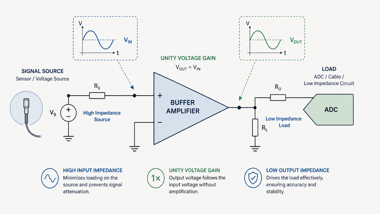 Buffer Amplifier Guide: How It Works, Key Specifications, Applications and Selection
16 June 2026139
 Low-Power Design of Operational Amplifiers
27 March 20256975
 Google Co-releases SayCan Model for Bots to Give Sensible Answers
30 August 20223784
 Introduction to Lead Acid Battery: Construction, Working Principle and Types
04 March 202110440
Analog Devices Inc.
In Stock: 924
Minimum: 1 Multiples: 1
Qty
Unit Price
Ext Price
1
$982.126649
$982.13
10
$926.534574
$9,265.35
100
$874.089221
$87,408.92
500
$824.612473
$412,306.24
1000
$777.936295
$777,936.30
Not the price you want? Send RFQ Now and we'll contact you ASAP.
Inquire for More Quantity
![ADV7513BSWZ]() ADV7513BSWZ
ADV7513BSWZAnalog Devices, Inc.
![AD9877ABSZ]() AD9877ABSZ
AD9877ABSZAnalog Devices, Inc.
![LTC2245CUH#TRPBF]() LTC2245CUH#TRPBF
LTC2245CUH#TRPBFLinear Technology/Analog Devices
![AD7791BRMZ-REEL]() AD7791BRMZ-REEL
AD7791BRMZ-REELAnalog Devices Inc.
![AD7799BRUZ-REEL]() AD7799BRUZ-REEL
AD7799BRUZ-REELAnalog Devices Inc.
![AD7190BRUZ-REEL]() AD7190BRUZ-REEL
AD7190BRUZ-REELAnalog Devices Inc.
![AD7705BRZ-REEL]() AD7705BRZ-REEL
AD7705BRZ-REELAnalog Devices Inc.
![AD7175-2BRUZ-RL7]() AD7175-2BRUZ-RL7
AD7175-2BRUZ-RL7Analog Devices Inc.
![AD7192BRUZ-REEL]() AD7192BRUZ-REEL
AD7192BRUZ-REELAnalog Devices Inc.
![AD9283BRSZ-RL100]() AD9283BRSZ-RL100
AD9283BRSZ-RL100Analog Devices Inc.


