
 Product
 Brand
Brand Articles
 Tools
Tools
NE555 VS TS555 Power Consumption[Video]

555 Type, Timer/Oscillator (Single) Programmable Timers NE555 8-DIP (0.300, 7.62mm)
Unit Price: $0.159985
Ext Price: $0.16


555 Type, Timer/Oscillator (Single) Programmable Timers NE555 8-DIP (0.300, 7.62mm)
NE555 and TS555 are all integrated circuits. This article is going to talk about the features, applications, and pinout of NE555 and TS555, and interpret the differences between them.

CMOS 555 Timer - TS555 vs NE555 Power Consumption
- Overview of NE555
- Overview of TS555
- NE555 VS TLC555 Features
- NE555 VS TS555 Pinout
- NE555 VS TS555 Schematic
- NE555 VS TS555 Block Diagram
- NE555 VS TS555 Absolute Maximum Ratings
- NE555 VS TS555 Specifications
- NE555 VS TS555 Specifications
- Conclusion of NE555 VS TS555
- NE555 VS TS555 Datasheet
- NE555 VS TS555 Package information
- Popularity by Region
Overview of NE555
The NE555 is a precision timing circuit capable of generating exact time delays or oscillation. In the time-delay or mono-stable mode of operation, the timed interval is regulated by a single external resistor and capacitor network. In the a-stable mode of operation, the frequency and duty cycle can be controlled independently using two external resistors and a single external capacitor. The output circuit of the NE555 can sink or source up to 200 milliamps of current. The operation is restricted to a voltage range of 5 to 15 volts. When powered by a 5-V supply, the output levels are compatible with TTL inputs.
Overview of TS555
The TS555 is a single CMOS timer with extremely low power consumption (Icc(TYP)TS555 = 110 A at VCC = +5 V versus Icc(TYP)NE555(a)= 3 mA) and high frequency (ff(max.) TS555 = 2.7 MHz versus f(max)NE555(a)= 0.1 MHz). Both monostable and astable modes maintain correct timing. The TS555 has lower supply current spikes during output transitions, allowing for the use of smaller decoupling capacitors than the bipolar NE555 (a). Timing capacitors can also be reduced thanks to the high input impedance (1012).
NE555 VS TLC555 Features
NE555 Features
Timing From Microseconds to Hours
Astable or Monostable Operation
Adjustable Duty Cycle
TTL-Compatible Output Can Sink or Source Up to 200 mA
On Products Compliant to MIL-PRF-38535. All Parameters Are Tested Unless Otherwise Noted. On All Other Products, Production Processing Does Not Necessarily Include Testing of All Parameters.
TS555 Features
Very low power consumption:
-110 μA typ at VCC= 5 V
-90 μa typ at VCC= 3 V
High maximum astable frequency of 2.7 MHz
Pin-to-pin functionally-compatible with bipolar NE555(a)
Wide voltage range: +2 V to +16 V
Supply current spikes are reduced during output transitions
High input impedance: 1012Ω
Output compatible with TTL, CMOS, and logic MOS
NE555 VS TS555 Pinout

NE555 Pinout

TS555 Pinout
NE555 VS TS555 Schematic

NE555 Schematic

TS555 Schematic
NE555 VS TS555 Block Diagram

NE555 Block Diagram

TS555 Block Diagram
NE555 VS TS555 Absolute Maximum Ratings
| MIN MAX | UNIT | ||
| VCC Supply voltage(2) | 18 | V | |
| VI Input voltage | CONT, RESET, THRES, TRIG | VCC | V |
| IO Output current | ±225 | mA | |
| θJA Package thermal impedance(3)(4) | D package | 97 | °C/W |
| P package | 85 | ||
| PS package | 95 | ||
| PW package | 149 | ||
| θJC Package thermal impedance(5)(6) | FK package | 5.61 | °C/W |
| JG package | 14.5 | ||
| TJ Operating virtual junction temperature | 150 | °C | |
| Case temperature for 60 s | FK package | 260 | °C |
| Lead temperature 1,6 mm (1/16 in) from the case for 60 s | JG package | 300 | °C |
NE555 Absolute Maximum Ratings
| Symbol | Parameter | Value | Unit |
| VCC | Supply voltage | + 18 | V |
| IOUT | Output current | ± 100 | mA |
| Rthja | Thermal resistance junction to ambient (1) | 125 | °C/W |
| Rthjc | Thermal resistance junction to case (1) | 40 | |
| TJ | Junction temperature | + 150 | °C |
| Tstg | Storage temperature range | -65 to +150 | |
| ESD | Human body model (HBM)(2) | 1500 | V |
| Machine model (MM)(3) | 200 | ||
| Charged device model (CDM)(4) | 1000 |
NE555 VS TS555 Specifications
NE555 VS TS555 Applications
NE555 Applications
Fingerprint Biometrics
Iris Biometrics
RFID Reader
TS555 Applications
The TS555 provides reduced supply current spikes during output transitions
NE555 VS TS555 Specifications
| TS555 | NE555 | |
| Attribute | Value | Value |
| Mounting Type | Through Hole | Surface Mount |
| Timer Type | Standard | Monostable |
| Package Type | PDIP | SO |
| Number of Internal Timers | 1 | 2 |
| Pin Count | 8 | 8 |
| Minimum Operating Supply Voltage | 4.5 V | 2 V |
| Maximum Operating Supply Voltage | 16 V | 16 V |
| Minimum Operating Temperature | 0 °C | -40 °C |
| Maximum Operating Temperature | +70 °C | +125 °C |
| Maximum Low-Level Output Current | 200mA | 1mA |
| Maximum High-Level Output Current | -200mA | -0.3mA |
| Height | 4.57mm | 1.5mm |
| Length | 9.81mm | 5mm |
| Dimensions | 9.81 x 6.35 x 4.57mm | 5 x 4 x 1.5mm |
| Width | 6.35mm | 4mm |
Conclusion of NE555 VS TS555
The TS555 is a single CMOS timer with low power consumption (Icc(TYP) TS555 = 110A at VCC=+5V versus Icc(TYP) NE555 = 3mA) and a high frequency (ff(max.) TS555 = 2.7MHz versus f(max.) NE555 = 0.1 MHz). As a result, whether in Monostable or Astable mode, timing is extremely precise. When compared to the bipolar NE555, the TS555 has lower supply current spikes during output transitions, allowing for the use of smaller decoupling capacitors. Due to the high input impedance (1012:9), timing capacitors can also be reduced.
The CMOS versions of the TS555 have lower source/sink current parameters than the TTL versions of the NE555. (ff(max)TS555 = 2.7 MHz vs. f(max)NE555(a)=0.1 MHz). Both monostable and astable modes maintain correct timing. The TS555 has lower supply current spikes during output transitions, allowing for the use of smaller decoupling capacitors than the bipolar NE555 (a).
NE555 VS TS555 Datasheet
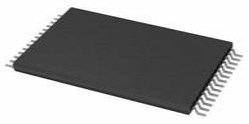
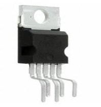
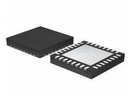
NE555 VS TS555 Package information

NE555 Package information
.png")
.png")
TS555 Package information
Popularity by Region
What is the use of NE555?
Modes. The following are the modes of operation for the 555 IC: In its astable (free-running) mode, the 555 can be utilized as an electronic oscillator. Just a few examples include LED and lamp flashers, pulse creation, logic clocks, tone production, security alarms, pulse-position modulation, and other applications.
What is the TS555?
The TS555 is a single CMOS timer with low power consumption (Icc(TYP) TS555 = 110 A at VCC = +5 V versus Icc(TYP) NE555 = 3 mA) and a high frequency (ff(max.) TS555 = 2.7 MHz versus f(max) NE555 = 0.1 MHz). Both monostable and astable modes maintain correct timing.
What is the use of TS555?
The TS555 has lower supply current spikes during output transitions, allowing for the use of smaller decoupling capacitors than the bipolar NE555 (a). Timing capacitors can also be reduced thanks to the high input impedance (1012).
What is the difference between NE555 and LM555?
They're both the same. The term "555" refers to a 555 timer IC in general. Signetics originally allocated the NE555 component number to the commercial temperature range variation (SE555 was the military temperature range type).
 ADC0804 ADC: Datasheet, Schematic, Pinout
09 October 202111864
 DS17285E-3+ Real Time Clock: Pinout, Equivalent and Datasheet
17 April 2025335
 dsPIC33EV32GM104 TIML: Digital Signal Controller Datasheet Overview
29 February 2024150
 L200CV: 40V, Voltage Regulator, Pinout and Datasheet
08 March 20223253
 LPC824 Microcontroller: Datasheet, Pinout, NXP LPC824
23 August 20211995
 74LS32 Quad-2-Input OR Gate: Datasheet pdf, Pinout and Circuit
22 November 202116579
 STM32L021K4T6 Ultra-Low-Power 32-bit MCU: Datasheet Analysis
29 February 2024163
 BCP56 Transistor: Features, Pinout, and Datasheet
13 October 20213107
 HIKSEMI Authorized Distributor | UTMEL Electronics
15 November 20233659
 MEMS Basics: System Features and Classifications
11 June 20216740
 VRLA Battery: Working Principle, Capacity and Maintenance
12 March 20219721
 Introduction to VOC Sensor
22 October 20215125
 BMW CEO: The Car Chip Problem Will Not Be Solved Until 2023
12 April 20225253
 What is Time Delay Relay?
18 December 202513634
 Is ON Semiconductor's Stock Overvalued? A Detailed Analysis
28 September 20233365
 Why is 50 ohms?
13 June 202210582
ON Semiconductor
In Stock: 79250
Minimum: 1 Multiples: 1
Qty
Unit Price
Ext Price
1
$0.159985
$0.16
500
$0.117636
$58.82
1000
$0.098030
$98.03
2000
$0.089936
$179.87
5000
$0.084052
$420.26
10000
$0.078188
$781.88
15000
$0.075617
$1,134.26
50000
$0.074353
$3,717.65
Not the price you want? Send RFQ Now and we'll contact you ASAP.
Inquire for More Quantity
![MC1455DR2G]() MC1455DR2G
MC1455DR2GON Semiconductor
![LM555CMX]() LM555CMX
LM555CMXON Semiconductor
![NCV1455BDR2G]() NCV1455BDR2G
NCV1455BDR2GON Semiconductor
![MC14536BDWR2G]() MC14536BDWR2G
MC14536BDWR2GON Semiconductor
![MC1455BDR2G]() MC1455BDR2G
MC1455BDR2GON Semiconductor
![MC14541BDR2G]() MC14541BDR2G
MC14541BDR2GON Semiconductor
![LM555CN]() LM555CN
LM555CNON Semiconductor
![LM555CM]() LM555CM
LM555CMON Semiconductor
![MC14541BDG]() MC14541BDG
MC14541BDGON Semiconductor
![MC1455P1G]() MC1455P1G
MC1455P1GON Semiconductor


