
 Product
 Brand
Brand Articles
 Tools
Tools
AD9257 Octal ADC Integration Notes: FPGA Timing, VCM Handling, and Alternatives


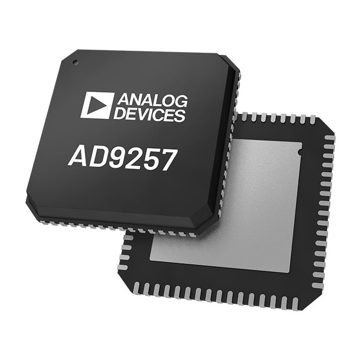
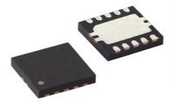
14 Bit 0.5mm ADC AD9257 1.8V 64-WFQFN Exposed Pad
Explore the AD9257 14-bit octal ADC. Learn how to resolve FPGA timing issues, handle VCM power-down conflicts, and evaluate alternatives like the AD9637.
- Core Specifications and Engineering Tradeoffs
- Resolving FPGA Timing and DCO Phase Alignment
- Chop Mode and Frequency Translation Realities
- VCM Pin Power-Down Handling
- Target Applications and System Fit
- Alternatives, Upgrades, and Competitors
- Datasheet, Package, and Schematic Verification
- Frequently Asked Questions
- Specifications
- Datasheet PDF
The AD9257 is an octal, 14-bit, 40 MSPS to 65 MSPS analog-to-digital converter (ADC) designed for high-density signal processing applications requiring precise dynamic performance and low power consumption. Featuring an on-chip sample-and-hold circuit, it is explicitly optimized for designs where PCB real estate is at a premium and thermal budgets are strictly capped.
When integrating eight high-speed data channels into a single package, engineers face a distinct set of challenges ranging from serial data alignment to crosstalk mitigation.
Market Position: A high-density, low-power solution for multi-channel acquisition.
Primary Interface: Serial LVDS (ANSI-644 default) with a reduced signal option.
Key Selection Factor: 55 mW per channel power consumption (at 65 MSPS) allows for tight packing in portable or enclosed systems.
Replacement Risk: While pin-compatible step-down options exist, moving to different architectures requires significant FPGA IP rewrites.
Core Specifications and Engineering Tradeoffs
Evaluating the AD9257 requires balancing its impressive dynamic performance against the physical realities of routing an octal ADC.
Resolution and Speed: 14-bit resolution operating between 40 MSPS and 65 MSPS.
Dynamic Performance: SNR of 75.5 dB and SFDR of 91.6 dBc (to Nyquist).
Power Consumption: 55 mW per channel at the maximum 65 MSPS rate, operating from a 1.8 V supply.
Input and Bandwidth: 2 V p-p input voltage range with a massive 650 MHz full power analog bandwidth.
The 650 MHz analog bandwidth is a double-edged sword. While it provides excellent headroom for undersampling applications and intermediate frequency (IF) processing, it heavily penalizes sloppy front-end design. Any broad-spectrum noise present at the inputs will alias down into your baseband unless aggressively band-limited. Engineers must implement stringent anti-aliasing filters and ensure pristine clock sources, as jitter on the sample clock will rapidly degrade the 75.5 dB SNR in high-frequency input scenarios.
Resolving FPGA Timing and DCO Phase Alignment
One of the most frequent integration hurdles with the AD9257 involves serial data capture at the receiving FPGA. Because the device multiplexes 14 bits of data per channel over Serial LVDS lines, the timing margins at 65 MSPS are exceptionally tight.
A common symptom of timing failure is the capture of bad data or corrupted digital test patterns when the input clock frequency is changed during development or dynamic operation. This occurs because the propagation delay through the ADC and the resulting phase relationship between the Data Clock Output (DCO) and the data lines shift.
To resolve this, engineers must actively manage the DCO phase. Instead of attempting complex delay-locked loop (DLL) adjustments entirely within the FPGA fabric, you can adjust the DCO phase directly at the ADC via SPI Register 0x16. Tuning this register shifts the DCO relative to the data frame, allowing you to center the clock edge squarely within the valid data eye. When shifting clock frequencies, always re-verify your test patterns (the AD9257 includes built-in and custom digital test pattern generation specifically for this purpose) and update Register 0x16 as needed to restore timing alignment.
Chop Mode and Frequency Translation Realities
The AD9257 includes a chop mode designed to mitigate low-frequency noise and offset anomalies, which is particularly useful in continuous-wave ultrasound or baseband receiver applications. However, there is a persistent misunderstanding regarding how chop mode interacts with the frequency spectrum.
Many engineers expect chop mode to shift the fundamental frequency spectrum line of their signal. This is incorrect. Chop mode does not translate fundamental frequencies if the signal resides entirely inside the first Nyquist zone. Spectrum lines will only translate via frequency folding if the input signal is outside the first Nyquist zone. If you are relying on chop mode to push 1/f noise away from a DC-coupled signal, ensure your digital down-conversion (DDC) or subsequent DSP stages are correctly configured to handle the specific folding behavior of your input band.
VCM Pin Power-Down Handling
The common-mode voltage (VCM) pin is critical for setting the DC bias of the analog inputs. The AD9257 provides an internal VCM reference, but many high-precision designs opt to drive this node with a low-noise external reference to match the front-end amplifier perfectly.
If you choose to use an external VCM source, there is a strict sequence required to avoid voltage conflicts and erratic power-draw behavior. You must promptly power down the internal VCM at start-up via SPI Register 0x102.
A frequent design error is treating the powered-down VCM pin exactly like an active one. When the internal VCM is powered down, the VCM pin does not need to be decoupled to ground. Leaving heavy decoupling capacitors on a disabled VCM pin while driving it externally can alter the startup time of your external reference and create unnecessary AC ground loops. Remove the local decoupling capacitors if the internal VCM is disabled.
Target Applications and System Fit
The AD9257’s combination of octal density and 55 mW/channel power draw naturally restricts it to specific, high-value applications where these traits justify the cost and layout complexity.
Medical Imaging and Ultrasound: Both non-destructive testing and portable medical ultrasound require massive channel counts (often 64 to 256 channels per probe head). The AD9257 allows designers to pack eight channels into a tiny footprint without exceeding the strict thermal limits of a handheld digital beam-forming system.
Quadrature and Diversity Radio Receivers: In phased array or MIMO communication setups, the phase coherence between the eight channels on a single die provides superior matching compared to synchronizing multiple discrete ADCs.
Optical Networking and Test Equipment: High-density instrumentation relies on the programmable clock and data alignment features to maintain channel-to-channel timing accuracy across complex backplanes.
Alternatives, Upgrades, and Competitors
When sourcing the AD9257 or designing a flexible BOM, evaluating alternatives is a mandatory step.
Pin-Compatible Downgrade:
The AD9637 is the most direct alternative. It is a pin-compatible 12-bit version of the AD9257. If your system's dynamic range requirements loosen, or if the 14-bit variant faces supply chain constraints, the AD9637 can be dropped into the exact same PCB footprint with minimal software changes, instantly reducing BOM cost.
Functional Competitors:
* AD9259 and AD9251: These are related Analog Devices converters. The AD9259 is a 14-bit quad ADC (50 MSPS), useful if you only need four channels and want to simplify routing.
* LTC2160, LTC2280, LTC2281: These Linear Technology (now Analog Devices) parts operate in similar resolution and speed tiers but feature different architectural tradeoffs, power profiles, and pinouts. Moving to an LTC part will require a complete PCB spin and an overhaul of the FPGA LVDS capture code.
Datasheet, Package, and Schematic Verification
Before finalizing your schematic capture, several critical physical and electrical parameters must be verified.
Thermal Pad Grounding: The AD9257 is packaged in a space-saving footprint that relies entirely on an exposed bottom paddle for thermal dissipation and electrical grounding. Confirm the exact thermal pad dimensions and via-stitching requirements in the latest spec sheet. A poorly soldered thermal pad will cause the device to overheat and degrade the SNR.
LVDS Termination: The device defaults to ANSI-644 standard LVDS. If your FPGA prefers a reduced signal swing to save power or reduce EMI, you must configure the ADC via SPI to use the reduced signal option. Ensure your 100-ohm differential termination resistors are placed as physically close to the FPGA receiver pins as possible.
Power Sequencing: Verify that the 1.8 V analog and digital supplies ramp smoothly. Since the device features both full-chip and individual channel power-down modes, ensure your microcontroller's startup routine does not inadvertently try to read data before the SPI configuration has fully awakened the required channels.
Frequently Asked Questions
Can I replace the AD9257 with the AD9637 without changing the PCB footprint?
Yes. The AD9637 is a pin-compatible 12-bit alternative. You can use the same PCB footprint and power supplies, though you will need to adjust your FPGA data parser to handle 12-bit words instead of 14-bit words.
Why is my FPGA capturing bad data frames when I change the ADC sample clock?
Changing the input clock frequency shifts the timing relationship between the serial data lines and the Data Clock Output (DCO). You must adjust the DCO phase via SPI register 0x16 to re-align the clock edge with the valid data eye for your specific frequency.
Do I need a decoupling capacitor on the VCM pin if I am using an external reference voltage?
No. If you are driving VCM externally, you must power down the internal VCM via SPI Register 0x102. Once powered down, the VCM pin does not require its own decoupling capacitor to ground.
Will chop mode shift the fundamental frequency of my input signal?
No. Chop mode does not translate fundamental frequencies within the first Nyquist zone. It only translates spectrum lines via frequency folding if your input signal sits outside the first Nyquist zone.
Specifications
Datasheet PDF
- Datasheets :
- ConflictMineralStatement :
 A Comprehensive Guide to LTC6601IUF-2#PBF Active Filter Interface
06 March 2024110
![How to Use BC547B Transistor as a Switch or an Amplifier?[ Video]](https://res.utmel.com/Images/Article/334c4527-7050-48e2-a137-ec8df881fc76.jpg) How to Use BC547B Transistor as a Switch or an Amplifier?[ Video]
How to Use BC547B Transistor as a Switch or an Amplifier?[ Video]07 April 20223604
 AD7768 Analog-to-Digital Converter (ADC): AD7768 Arduino, Datasheet, Pinout
18 January 20227628
 SMAJ15A TVs Diodes: Features, Pinout, and Datasheet
15 February 20223210
 BC108 Transistor: Pinout, Datasheet, and Equivalent
20 November 202114387
 TPS51200DRCR Regulator: Features, Applications and Datasheet
28 October 20231632
 ATTINY85 Microcontroller: Datasheet , Applications and Pinout
23 September 202312197
![AT89C2051-24PU 8-bit Microcontroller: Circuit Diagram, Pinout, and Datasheet [Video&FAQ]](https://res.utmel.com/Images/Article/789f3a55-d7a1-41ca-9784-35cc175f9498.png) AT89C2051-24PU 8-bit Microcontroller: Circuit Diagram, Pinout, and Datasheet [Video&FAQ]
AT89C2051-24PU 8-bit Microcontroller: Circuit Diagram, Pinout, and Datasheet [Video&FAQ]16 February 202214905
 How to Check 2073 Transistor Pinout at Home
01 September 20253625
 Application of Wide Bandgap Devices in EV Converters
12 April 20231302
 Introduction to BGA Package
07 December 20215647
 Rectangular Connectors vs Circular Connectors: Which fits your Project Best
04 July 20252619
 What is a Wireless Network Adapter?
01 June 20216801
 HF PCB Circuit Design 10 Questions
16 March 20225330
 When Designing a Power Supply, How to Consider the Selection of Topology?
07 March 20224432
 Top 10 High-Performance End Mills for Metalworking in 2025
17 July 20254463
Analog Devices Inc.
In Stock
United States
China
Canada
Japan
Russia
Germany
United Kingdom
Singapore
Italy
Hong Kong(China)
Taiwan(China)
France
Korea
Mexico
Netherlands
Malaysia
Austria
Spain
Switzerland
Poland
Thailand
Vietnam
India
United Arab Emirates
Afghanistan
Åland Islands
Albania
Algeria
American Samoa
Andorra
Angola
Anguilla
Antigua & Barbuda
Argentina
Armenia
Aruba
Australia
Azerbaijan
Bahamas
Bahrain
Bangladesh
Barbados
Belarus
Belgium
Belize
Benin
Bermuda
Bhutan
Bolivia
Bonaire, Sint Eustatius and Saba
Bosnia & Herzegovina
Botswana
Brazil
British Indian Ocean Territory
British Virgin Islands
Brunei
Bulgaria
Burkina Faso
Burundi
Cabo Verde
Cambodia
Cameroon
Cayman Islands
Central African Republic
Chad
Chile
Christmas Island
Cocos (Keeling) Islands
Colombia
Comoros
Congo
Congo (DRC)
Cook Islands
Costa Rica
Côte d’Ivoire
Croatia
Cuba
Curaçao
Cyprus
Czechia
Denmark
Djibouti
Dominica
Dominican Republic
Ecuador
Egypt
El Salvador
Equatorial Guinea
Eritrea
Estonia
Eswatini
Ethiopia
Falkland Islands
Faroe Islands
Fiji
Finland
French Guiana
French Polynesia
Gabon
Gambia
Georgia
Ghana
Gibraltar
Greece
Greenland
Grenada
Guadeloupe
Guam
Guatemala
Guernsey
Guinea
Guinea-Bissau
Guyana
Haiti
Honduras
Hungary
Iceland
Indonesia
Iran
Iraq
Ireland
Isle of Man
Israel
Jamaica
Jersey
Jordan
Kazakhstan
Kenya
Kiribati
Kosovo
Kuwait
Kyrgyzstan
Laos
Latvia
Lebanon
Lesotho
Liberia
Libya
Liechtenstein
Lithuania
Luxembourg
Macao(China)
Madagascar
Malawi
Maldives
Mali
Malta
Marshall Islands
Martinique
Mauritania
Mauritius
Mayotte
Micronesia
Moldova
Monaco
Mongolia
Montenegro
Montserrat
Morocco
Mozambique
Myanmar
Namibia
Nauru
Nepal
New Caledonia
New Zealand
Nicaragua
Niger
Nigeria
Niue
Norfolk Island
North Korea
North Macedonia
Northern Mariana Islands
Norway
Oman
Pakistan
Palau
Palestinian Authority
Panama
Papua New Guinea
Paraguay
Peru
Philippines
Pitcairn Islands
Portugal
Puerto Rico
Qatar
Réunion
Romania
Rwanda
Samoa
San Marino
São Tomé & Príncipe
Saudi Arabia
Senegal
Serbia
Seychelles
Sierra Leone
Sint Maarten
Slovakia
Slovenia
Solomon Islands
Somalia
South Africa
South Sudan
Sri Lanka
St Helena, Ascension, Tristan da Cunha
St. Barthélemy
St. Kitts & Nevis
St. Lucia
St. Martin
St. Pierre & Miquelon
St. Vincent & Grenadines
Sudan
Suriname
Svalbard & Jan Mayen
Sweden
Syria
Tajikistan
Tanzania
Timor-Leste
Togo
Tokelau
Tonga
Trinidad & Tobago
Tunisia
Turkey
Turkmenistan
Turks & Caicos Islands
Tuvalu
U.S. Outlying Islands
U.S. Virgin Islands
Uganda
Ukraine
Uruguay
Uzbekistan
Vanuatu
Vatican City
Venezuela
Wallis & Futuna
Yemen
Zambia
Zimbabwe
![ADV7513BSWZ]() ADV7513BSWZ
ADV7513BSWZAnalog Devices, Inc.
![AD9877ABSZ]() AD9877ABSZ
AD9877ABSZAnalog Devices, Inc.
![LTC2245CUH#TRPBF]() LTC2245CUH#TRPBF
LTC2245CUH#TRPBFLinear Technology/Analog Devices
![AD7791BRMZ-REEL]() AD7791BRMZ-REEL
AD7791BRMZ-REELAnalog Devices Inc.
![AD7799BRUZ-REEL]() AD7799BRUZ-REEL
AD7799BRUZ-REELAnalog Devices Inc.
![AD7190BRUZ-REEL]() AD7190BRUZ-REEL
AD7190BRUZ-REELAnalog Devices Inc.
![AD7705BRZ-REEL]() AD7705BRZ-REEL
AD7705BRZ-REELAnalog Devices Inc.
![AD7175-2BRUZ-RL7]() AD7175-2BRUZ-RL7
AD7175-2BRUZ-RL7Analog Devices Inc.
![AD7192BRUZ-REEL]() AD7192BRUZ-REEL
AD7192BRUZ-REELAnalog Devices Inc.
![AD9283BRSZ-RL100]() AD9283BRSZ-RL100
AD9283BRSZ-RL100Analog Devices Inc.


