
 Product
 Brand
Brand Articles
 Tools
Tools
AD5420 16-Bit DAC Design Notes: Managing Thermal Limits, HART Slew Rates, and 4-20mA Loops


5V V DAC Current - Buffered Surface Mount R-2R R 2 B B
Discover integration notes for the AD5420 16-bit DAC. Learn how to manage 4-20mA loops, solve HART network disruptions, and handle thermal limits in PLC designs.
- Key Electrical Characteristics for Process Control
- Managing Thermal Dissipation in High-Voltage Loops
- Solving HART Communication Disruption
- Surviving Hi-Pot Testing: Output Range Shifts
- Troubleshooting Unexpected /FAULT Line Activations
- Alternatives, Equivalents, and Replacement Considerations
- Datasheet, Package, and Ordering Verification
- Hyper-Specific FAQs
- Specifications
- Parts with Similar Specs
- Datasheet PDF
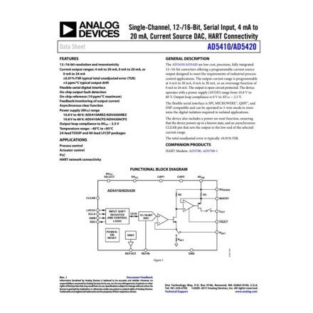
The AD5420 is a 16-bit digital-to-analog converter (DAC) designed for programmable current source outputs in industrial process control applications. Because industrial environments demand high reliability over long cable runs, designing with a precision current-source DAC requires more than just connecting SPI lines. Engineers must account for loop compliance, harsh factory transients, and thermal dissipation limits when driving high currents from high-voltage rails.
Market Position: A low-cost, fully integrated solution specifically tailored for programmable logic controllers (PLCs), actuator control, and process automation.
Core Selection Factor: Integrates an on-chip reference and fault detection, reducing the external bill of materials (BOM) for standard 4–20 mA, 0–20 mA, and 0–24 mA loops.
Integration Risk: High power dissipation when sourcing maximum current from a 60V supply requires strict thermal derating and careful PCB layout.
Key Electrical Characteristics for Process Control
When evaluating the AD5420 for an industrial module, the primary focus is on accuracy over temperature and power supply flexibility. The device guarantees 16-bit resolution and monotonicity, which is critical for smooth actuator positioning without hunting or oscillation.
Output Current Ranges: The device supports the standard 4-20 mA range for traditional industrial loops, as well as 0-20 mA and an over-range 0-24 mA setting. The 24 mA range is particularly useful for signaling out-of-band alarm conditions to a central controller.
Total Unadjusted Error (TUE): Rated at a typical ±0.01% of Full Scale Range (FSR). This minimizes the need for extensive multi-point factory calibration in standard applications.
Output Drift: At ±3 ppm/°C typical, the DAC maintains highly stable output across its -40°C to +85°C operating range. The on-chip reference itself is rated for a maximum of 10 ppm/°C, which is sufficient for most standard PLC analog output modules without requiring an external precision reference.
Supply Voltage (AVDD): The part is split into two distinct voltage ratings based on the ordering code. The AREZ variant supports 10.8 V to 40 V, while the ACPZ variant can handle up to 60 V.
Managing Thermal Dissipation in High-Voltage Loops
One of the most critical engineering compromises when designing with the AD5420 is managing the thermal load. While the device can source 24 mA and can operate from a 60 V supply (in the ACPZ version), doing both simultaneously forces the silicon to dissipate an immense amount of power.
If your AVDD is 60V and the load resistance is very low (e.g., a short circuit or a low-impedance receiver), the internal output transistor drops the majority of that voltage. Sourcing 24 mA across a 60 V drop results in nearly 1.44 W of localized power dissipation on the chip. Without mitigation, this will rapidly cause the junction temperature to exceed the 125°C maximum absolute rating, triggering thermal shutdown or permanent silicon degradation.
To fix this, you must de-rate the power dissipated directly on the chip. This is typically achieved by transferring the heat burden to the PCB or an external component. Using the LFCSP package is highly recommended for these high-power scenarios, as it provides a much lower thermal impedance (28°C/W) compared to standard TSSOPs, provided the exposed thermal pad is soldered to a substantial copper ground plane. In extreme cases, adding a series drop resistor outside the feedback loop can help absorb some of the voltage drop, keeping the DAC's internal dissipation within safe operating limits. Exact thermal derating will depend heavily on your PCB copper area, copper thickness, and ambient enclosure temperature, so running a thermal model during the layout phase is strictly required here.
Solving HART Communication Disruption
For environments utilizing the Highway Addressable Remote Transducer (HART) protocol, the AD5420 presents a specific integration challenge. The DAC's natural, unconstrained slew rate from 4 mA to 20 mA is approximately 10 µs. This extremely fast current transition generates high-frequency harmonics that can cause major disruption to a HART network, drowning out the 1.2 kHz and 2.2 kHz FSK signals used by the protocol.
To maintain HART compliance and prevent communication dropouts, the slew rate must be artificially slowed down. The AD5420 provides two mechanisms to achieve this:
Hardware Slew Rate Control: You must add external capacitors at the CAP1 and CAP2 pins. These capacitors directly limit the rate of change of the output current.
Digital Slew Rate Control: The device includes an internal digital slew rate control function accessible via the SPI interface. Enabling this allows the DAC to step through the output codes gradually rather than making a single massive jump.
Using a combination of both the external capacitors and the internal digital stepping is the most robust way to guarantee the output transitions smoothly without corrupting the HART network layer.
Surviving Hi-Pot Testing: Output Range Shifts
Industrial equipment must frequently undergo High Potential (Hi-Pot) testing to verify isolation barriers. A known pain point with the AD5420 is that the high voltage transients generated during aggressive Hi-Pot testing can couple into the device and corrupt the internal calibration registers.
When these registers are corrupted, the microprocessor loses its calibration framing, causing the output to shift abnormally high—sometimes driving the loop up to 134 mA, completely saturating the receiver and potentially damaging downstream equipment.
If your module must survive repeated Hi-Pot testing, you cannot rely on the bare DAC. You must design external protection. Adding external protection diodes (such as TVS arrays) and surge current limiting resistors on the output lines is mandatory. If a transient does manage to lock up the device, you can execute a hard hardware reset by briefly shorting the R3sense output to ground; this collapses the AVDD supply locally and forces the internal microprocessor to reset and reload its default states.
Troubleshooting Unexpected /FAULT Line Activations
The AD5420 includes an active-low /FAULT pin designed to alert the host microcontroller of over-temperature conditions or broken output loops (IOut faults). However, during prototyping, engineers often encounter unexpected /FAULT line activations even when the ambient temperature is normal and the loop appears connected.
If this occurs, investigate the output loop compliance voltage. The AD5420 requires a compliance headroom of AVDD − 2.5 V. This means if your AVDD is 24 V, the maximum voltage that can be developed across your load resistor is 21.5 V. If your load resistance is too high (e.g., 1 kΩ) and you attempt to drive 24 mA, the required voltage (24 V) exceeds the compliance limit (21.5 V). The internal driver starves for voltage, fails to reach the target current, and correctly flags an IOut fault.
Always verify your maximum load resistor against your minimum expected AVDD supply, and double-check your slew-rate settings, as overly aggressive capacitive loads can momentarily trigger the fault comparator during fast transitions.
Alternatives, Equivalents, and Replacement Considerations
When navigating supply chain constraints or looking for feature upgrades, several direct competitors and sister parts exist. Be aware that "equivalents" in precision analog are rarely drop-in replacements without some firmware or layout adjustments.
Analog Devices AD5422: The most direct upgrade path. The AD5422 is essentially the same core architecture but adds a programmable voltage output alongside the current output. If you are migrating from an AD5420 to an AD5422 due to stock shortages, the footprint is often compatible, but you must ensure your firmware does not accidentally enable the voltage output stage into a pure current loop.
Analog Devices AD5421: This is a loop-powered, 16-bit, 4-20 mA DAC. Unlike the AD5420, which is locally powered by a separate AVDD supply, the AD5421 extracts its operating power directly from the 4-20 mA loop itself. It is not a drop-in replacement, but it is the correct architectural choice if you are designing a 2-wire transmitter rather than a 3-wire/4-wire PLC output module.
Texas Instruments DAC8750: A strong competitor in the industrial 4-20 mA space. It offers similar 16-bit resolution and programmable current ranges. Switching to the DAC8750 requires a complete PCB footprint redesign and a rewrite of the SPI driver, as the register maps and internal fault handling differ significantly.
Analog Devices AD420: An older generation, legacy 16-bit current-output DAC. It lacks the advanced fault detection and flexible digital slew rate control of the AD5420. It should generally not be considered for new designs, but you may see it in legacy BOMs being upgraded to the AD5420.
Datasheet, Package, and Ordering Verification
Before finalizing your schematic symbol and footprint library, pay close attention to the ordering suffix, as it dictates both package type and absolute maximum ratings.
Voltage Limits: As noted, the
AREZsuffix indicates a lower maximum supply voltage (40 V), while theACPZsuffix handles up to 60 V. Do not mix these up in your BOM, or a 48 V industrial rail will instantly destroy an AREZ-rated part.Package Types: The ACPZ variant utilizes the LFCSP (Lead Frame Chip Scale Package). When verifying your EDA footprint, you must ensure the center thermal pad is present, correctly sized, and stitched with vias to a large internal ground plane. The device relies entirely on this pad to achieve its 28°C/W thermal resistance.
Digital Interface: Verify your microcontroller's SPI mode. The AD5420 features a flexible serial digital interface compatible with standard SPI, MICROWIRE, QSPI, and DSP protocols, but ensuring your clock polarity (CPOL) and phase (CPHA) match the datasheet timing diagrams will save hours of firmware debugging. An asynchronous clear function is also provided—ensure this pin is tied off correctly if unused to prevent spurious output resets in noisy environments.
Hyper-Specific FAQs
Why does my AD5420 output jump to 134mA after factory isolation testing?High voltage transients during Hi-Pot testing can couple into the device and corrupt the internal calibration registers. This loss of calibration causes the output to shift abnormally high. You must add external protection diodes and surge resistors to the output path, or briefly short the R3sense pin to ground to collapse AVDD and force a hard reset.
Why is the /FAULT pin triggering when I output 20mA, even though the loop is closed?You are likely violating the output loop compliance voltage. The maximum voltage you can drive across your load is AVDD − 2.5 V. If your AVDD drops due to supply sag, or if your load resistance is too high, the DAC cannot physically push 20 mA through the loop. The driver saturates and triggers the fault line.
Can I use the AD5420 on a HART network without external capacitors?No. The natural slew rate of the AD5420 is 10 µs, which is far too fast and will generate harmonics that disrupt HART communications. You must use external capacitors on the CAP1 and CAP2 pins, combined with the internal digital slew rate control, to smooth the transitions.
Why is my AD5420 overheating when running off a 48V supply?Power dissipation is calculated as the voltage dropped across the DAC multiplied by the current. Sourcing 24 mA from a 48 V supply into a low-impedance load forces the DAC to dissipate over 1 Watt. You must de-rate the power, ensure you are using the LFCSP package with a proper thermal ground plane, or add a series drop resistor to share the thermal load.
Watch Tutorial: AD5420
Specifications
Parts with Similar Specs
- ImagePart NumberManufacturerPackage / CaseNumber of PinsNumber of BitsSettling TimeInterfacePolarityNumber of ChannelsNumber of DAC ChannelsMin Supply VoltageView Compare
![AD5420AREZ-REEL7]()
AD5420AREZ-REEL7
24-TSSOP (0.173, 4.40mm Width) Exposed Pad
24
16
40μs
SPI, Serial
Unipolar
1
1
10.8 V
![AD5422AREZ]()
24-TSSOP (0.173, 4.40mm Width) Exposed Pad
24
12
40μs
SPI, Serial
Unipolar
-
-
10.8 V
![AD5410AREZ]()
24-TSSOP (0.173, 4.40mm Width) Exposed Pad
24
16
25μs (V), 40μs (A) (Typ)
SPI, Serial
Bipolar, Unipolar
-
-
10.8 V
![AD5422BREZ]()
24-TSSOP (0.173, 4.40mm Width) Exposed Pad
24
16
25μs (V), 40μs (A) (Typ)
SPI, Serial
Bipolar, Unipolar
-
-
10.8 V
![TLV5619IPW]()
20-TSSOP (0.173, 4.40mm Width)
20
12
3μs
-
Unipolar
-
-
2.7 V


Datasheet PDF
- Datasheets :
- Other Related Documents :
- ConflictMineralStatement :
 Microchip PIC32MX664F128HIPT Microcontroller Datasheet Overview
29 February 2024132
 ADA4817 Amplifier: Datasheet, Pinout and Applications
13 August 20213196
 Renesas RX24U Group Microcontroller: Advancements and Applications
29 February 2024156
 dsPIC33FJ128GP206: High-Performance Digital Signal Controller Overview
28 February 2024113
 XC1701 Series 1-Mbit Serial Configuration PROM: Technical Guide and Legacy Support
14 January 2026106
 LM3915 Dot/Bar Display Driver: Circuit, Price and Application
29 July 20215466
 Microchip PIC16LF1516ISP: A Comprehensive Overview of Features and Applications
29 February 2024270
 LM4041 Bandgap Circuit: Pinout, Features and Datasheet
05 November 2021943
 Basic Introduction to System on a Chip
02 December 20204328
 Analog Switch: Types and Application
25 March 202114973
 The Historical Milestones of Coaxial Cable Development
19 July 20252728
 Detailed Analysis of Analog IC
22 November 20213629
 Why Precision Matters in Analog-to-Digital Conversion
28 May 2025859
 2 Semiconductor Stocks to Buy Hand Over Fist in 2024 and 1 to Avoid Like the Plague
18 December 20234312
 Introduction to EPROM and EEPROM
08 January 202616324
 How to Select a Power Relay That Fits Your Requirements
10 July 20252747
Analog Devices Inc.
In Stock: 1000
United States
China
Canada
Japan
Russia
Germany
United Kingdom
Singapore
Italy
Hong Kong(China)
Taiwan(China)
France
Korea
Mexico
Netherlands
Malaysia
Austria
Spain
Switzerland
Poland
Thailand
Vietnam
India
United Arab Emirates
Afghanistan
Åland Islands
Albania
Algeria
American Samoa
Andorra
Angola
Anguilla
Antigua & Barbuda
Argentina
Armenia
Aruba
Australia
Azerbaijan
Bahamas
Bahrain
Bangladesh
Barbados
Belarus
Belgium
Belize
Benin
Bermuda
Bhutan
Bolivia
Bonaire, Sint Eustatius and Saba
Bosnia & Herzegovina
Botswana
Brazil
British Indian Ocean Territory
British Virgin Islands
Brunei
Bulgaria
Burkina Faso
Burundi
Cabo Verde
Cambodia
Cameroon
Cayman Islands
Central African Republic
Chad
Chile
Christmas Island
Cocos (Keeling) Islands
Colombia
Comoros
Congo
Congo (DRC)
Cook Islands
Costa Rica
Côte d’Ivoire
Croatia
Cuba
Curaçao
Cyprus
Czechia
Denmark
Djibouti
Dominica
Dominican Republic
Ecuador
Egypt
El Salvador
Equatorial Guinea
Eritrea
Estonia
Eswatini
Ethiopia
Falkland Islands
Faroe Islands
Fiji
Finland
French Guiana
French Polynesia
Gabon
Gambia
Georgia
Ghana
Gibraltar
Greece
Greenland
Grenada
Guadeloupe
Guam
Guatemala
Guernsey
Guinea
Guinea-Bissau
Guyana
Haiti
Honduras
Hungary
Iceland
Indonesia
Iran
Iraq
Ireland
Isle of Man
Israel
Jamaica
Jersey
Jordan
Kazakhstan
Kenya
Kiribati
Kosovo
Kuwait
Kyrgyzstan
Laos
Latvia
Lebanon
Lesotho
Liberia
Libya
Liechtenstein
Lithuania
Luxembourg
Macao(China)
Madagascar
Malawi
Maldives
Mali
Malta
Marshall Islands
Martinique
Mauritania
Mauritius
Mayotte
Micronesia
Moldova
Monaco
Mongolia
Montenegro
Montserrat
Morocco
Mozambique
Myanmar
Namibia
Nauru
Nepal
New Caledonia
New Zealand
Nicaragua
Niger
Nigeria
Niue
Norfolk Island
North Korea
North Macedonia
Northern Mariana Islands
Norway
Oman
Pakistan
Palau
Palestinian Authority
Panama
Papua New Guinea
Paraguay
Peru
Philippines
Pitcairn Islands
Portugal
Puerto Rico
Qatar
Réunion
Romania
Rwanda
Samoa
San Marino
São Tomé & Príncipe
Saudi Arabia
Senegal
Serbia
Seychelles
Sierra Leone
Sint Maarten
Slovakia
Slovenia
Solomon Islands
Somalia
South Africa
South Sudan
Sri Lanka
St Helena, Ascension, Tristan da Cunha
St. Barthélemy
St. Kitts & Nevis
St. Lucia
St. Martin
St. Pierre & Miquelon
St. Vincent & Grenadines
Sudan
Suriname
Svalbard & Jan Mayen
Sweden
Syria
Tajikistan
Tanzania
Timor-Leste
Togo
Tokelau
Tonga
Trinidad & Tobago
Tunisia
Turkey
Turkmenistan
Turks & Caicos Islands
Tuvalu
U.S. Outlying Islands
U.S. Virgin Islands
Uganda
Ukraine
Uruguay
Uzbekistan
Vanuatu
Vatican City
Venezuela
Wallis & Futuna
Yemen
Zambia
Zimbabwe
![AD5362BSTZ]() AD5362BSTZ
AD5362BSTZAnalog Devices Inc.
![AD7524LPZ]() AD7524LPZ
AD7524LPZAnalog Devices Inc.
![AD5328BRUZ-REEL7]() AD5328BRUZ-REEL7
AD5328BRUZ-REEL7Analog Devices Inc.
![ADV7125JSTZ330]() ADV7125JSTZ330
ADV7125JSTZ330Analog Devices Inc.
![AD5324ARMZ-REEL7]() AD5324ARMZ-REEL7
AD5324ARMZ-REEL7Analog Devices Inc.
![AD420ANZ-32]() AD420ANZ-32
AD420ANZ-32Analog Devices Inc.
![AD5304ARMZ]() AD5304ARMZ
AD5304ARMZAnalog Devices Inc.
![AD5683RBRMZ-3-RL7]() AD5683RBRMZ-3-RL7
AD5683RBRMZ-3-RL7Analog Devices Inc.
![AD5601BKSZ-REEL7]() AD5601BKSZ-REEL7
AD5601BKSZ-REEL7Analog Devices Inc.


