
 Product
 Brand
Brand Articles
 Tools
Tools
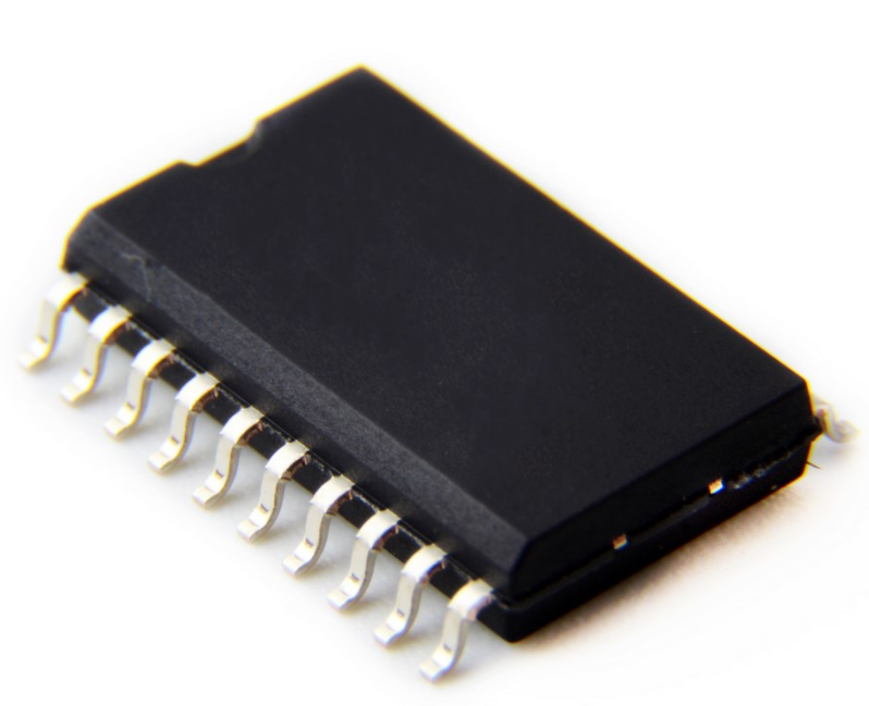
ADA4817 Amplifier: Datasheet, Pinout and Applications

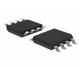
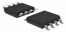
1 Channels 40mA per Channel 2pA -90 dB Instrumentational OP Amps 0.00002μA 5V~10V ±2.5V~5V ADA4817 8 Pins 8-SOIC (0.154, 3.90mm Width) Exposed Pad


1 Channels 40mA per Channel 2pA -90 dB Instrumentational OP Amps 0.00002μA 5V~10V ±2.5V~5V ADA4817 8 Pins 8-SOIC (0.154, 3.90mm Width) Exposed Pad
The ADA4817 amplifier is a kind of unity-gain stable, ultrahigh-speed, voltage feedback amplifier with FET inputs. This article enforces datasheet, pinout, applications, and other details about ADA4817.
ADA4817 Pinout


ADA4817 Description
The ADA4817 amplifier is a kind of unity-gain stable, ultrahigh-speed, voltage feedback amplifier with FET inputs. The ADA4817 amplifier was developed with the Analog Devices, Inc., proprietary extra fast complementary bipolar (XFCB) process, which allows the amplifiers to achieve ultralow noise (4 nV/√Hz; 2.5 fA/√Hz) as well as very high input impedances.
ADA4817 CAD Model
Footprint

3D Model

Specifications
- TypeParameter
- Lifecycle Status
Lifecycle Status refers to the current stage of an electronic component in its product life cycle, indicating whether it is active, obsolete, or transitioning between these states. An active status means the component is in production and available for purchase. An obsolete status indicates that the component is no longer being manufactured or supported, and manufacturers typically provide a limited time frame for support. Understanding the lifecycle status is crucial for design engineers to ensure continuity and reliability in their projects.
PRODUCTION (Last Updated: 3 weeks ago) - Factory Lead Time8 Weeks
- Mounting Type
The "Mounting Type" in electronic components refers to the method used to attach or connect a component to a circuit board or other substrate, such as through-hole, surface-mount, or panel mount.
Surface Mount - Package / Case
refers to the protective housing that encases an electronic component, providing mechanical support, electrical connections, and thermal management.
8-SOIC (0.154, 3.90mm Width) Exposed Pad - Surface Mount
having leads that are designed to be soldered on the side of a circuit board that the body of the component is mounted on.
YES - Number of Pins8
- Operating Temperature
The operating temperature is the range of ambient temperature within which a power supply, or any other electrical equipment, operate in. This ranges from a minimum operating temperature, to a peak or maximum operating temperature, outside which, the power supply may fail.
-40°C~105°C - Packaging
Semiconductor package is a carrier / shell used to contain and cover one or more semiconductor components or integrated circuits. The material of the shell can be metal, plastic, glass or ceramic.
Tube - Series
In electronic components, the "Series" refers to a group of products that share similar characteristics, designs, or functionalities, often produced by the same manufacturer. These components within a series typically have common specifications but may vary in terms of voltage, power, or packaging to meet different application needs. The series name helps identify and differentiate between various product lines within a manufacturer's catalog.
FastFET™ - JESD-609 Code
The "JESD-609 Code" in electronic components refers to a standardized marking code that indicates the lead-free solder composition and finish of electronic components for compliance with environmental regulations.
e3 - Pbfree Code
The "Pbfree Code" parameter in electronic components refers to the code or marking used to indicate that the component is lead-free. Lead (Pb) is a toxic substance that has been widely used in electronic components for many years, but due to environmental concerns, there has been a shift towards lead-free alternatives. The Pbfree Code helps manufacturers and users easily identify components that do not contain lead, ensuring compliance with regulations and promoting environmentally friendly practices. It is important to pay attention to the Pbfree Code when selecting electronic components to ensure they meet the necessary requirements for lead-free applications.
no - Part Status
Parts can have many statuses as they progress through the configuration, analysis, review, and approval stages.
Active - Moisture Sensitivity Level (MSL)
Moisture Sensitivity Level (MSL) is a standardized rating that indicates the susceptibility of electronic components, particularly semiconductors, to moisture-induced damage during storage and the soldering process, defining the allowable exposure time to ambient conditions before they require special handling or baking to prevent failures
3 (168 Hours) - Number of Terminations8
- ECCN Code
An ECCN (Export Control Classification Number) is an alphanumeric code used by the U.S. Bureau of Industry and Security to identify and categorize electronic components and other dual-use items that may require an export license based on their technical characteristics and potential for military use.
EAR99 - Terminal Finish
Terminal Finish refers to the surface treatment applied to the terminals or leads of electronic components to enhance their performance and longevity. It can improve solderability, corrosion resistance, and overall reliability of the connection in electronic assemblies. Common finishes include nickel, gold, and tin, each possessing distinct properties suitable for various applications. The choice of terminal finish can significantly impact the durability and effectiveness of electronic devices.
Matte Tin (Sn) - Terminal Position
In electronic components, the term "Terminal Position" refers to the physical location of the connection points on the component where external electrical connections can be made. These connection points, known as terminals, are typically used to attach wires, leads, or other components to the main body of the electronic component. The terminal position is important for ensuring proper connectivity and functionality of the component within a circuit. It is often specified in technical datasheets or component specifications to help designers and engineers understand how to properly integrate the component into their circuit designs.
DUAL - Terminal Form
Occurring at or forming the end of a series, succession, or the like; closing; concluding.
GULL WING - Peak Reflow Temperature (Cel)
Peak Reflow Temperature (Cel) is a parameter that specifies the maximum temperature at which an electronic component can be exposed during the reflow soldering process. Reflow soldering is a common method used to attach electronic components to a circuit board. The Peak Reflow Temperature is crucial because it ensures that the component is not damaged or degraded during the soldering process. Exceeding the specified Peak Reflow Temperature can lead to issues such as component failure, reduced performance, or even permanent damage to the component. It is important for manufacturers and assemblers to adhere to the recommended Peak Reflow Temperature to ensure the reliability and functionality of the electronic components.
260 - Number of Functions1
- Supply Voltage
Supply voltage refers to the electrical potential difference provided to an electronic component or circuit. It is crucial for the proper operation of devices, as it powers their functions and determines performance characteristics. The supply voltage must be within specified limits to ensure reliability and prevent damage to components. Different electronic devices have specific supply voltage requirements, which can vary widely depending on their design and intended application.
5V - Time@Peak Reflow Temperature-Max (s)
Time@Peak Reflow Temperature-Max (s) refers to the maximum duration that an electronic component can be exposed to the peak reflow temperature during the soldering process, which is crucial for ensuring reliable solder joint formation without damaging the component.
30 - Base Part Number
The "Base Part Number" (BPN) in electronic components serves a similar purpose to the "Base Product Number." It refers to the primary identifier for a component that captures the essential characteristics shared by a group of similar components. The BPN provides a fundamental way to reference a family or series of components without specifying all the variations and specific details.
ADA4817 - Pin Count
a count of all of the component leads (or pins)
8 - Number of Channels1
- Operating Supply Current
Operating Supply Current, also known as supply current or quiescent current, is a crucial parameter in electronic components that indicates the amount of current required for the device to operate under normal conditions. It represents the current drawn by the component from the power supply while it is functioning. This parameter is important for determining the power consumption of the component and is typically specified in datasheets to help designers calculate the overall power requirements of their circuits. Understanding the operating supply current is essential for ensuring proper functionality and efficiency of electronic systems.
21mA - Nominal Supply Current
Nominal current is the same as the rated current. It is the current drawn by the motor while delivering rated mechanical output at its shaft.
21mA - Output Current
The rated output current is the maximum load current that a power supply can provide at a specified ambient temperature. A power supply can never provide more current that it's rated output current unless there is a fault, such as short circuit at the load.
70mA - Quiescent Current
The quiescent current is defined as the current level in the amplifier when it is producing an output of zero.
21mA - Slew Rate
the maximum rate of output voltage change per unit time.
870V/μs - Amplifier Type
Amplifier Type refers to the classification or categorization of amplifiers based on their design, functionality, and characteristics. Amplifiers are electronic devices that increase the amplitude of a signal, such as voltage or current. The type of amplifier determines its specific application, performance capabilities, and operating characteristics. Common types of amplifiers include operational amplifiers (op-amps), power amplifiers, audio amplifiers, and radio frequency (RF) amplifiers. Understanding the amplifier type is crucial for selecting the right component for a particular circuit or system design.
Voltage Feedback - Common Mode Rejection Ratio
Common Mode Rejection Ratio (CMRR) is a measure of the ability of a differential amplifier to reject input signals that are common to both input terminals. It is defined as the ratio of the differential gain to the common mode gain. A high CMRR indicates that the amplifier can effectively eliminate noise and interference that affects both inputs simultaneously, enhancing the fidelity of the amplified signal. CMRR is typically expressed in decibels (dB), with higher values representing better performance in rejecting common mode signals.
-90 dB - Current - Input Bias
The parameter "Current - Input Bias" in electronic components refers to the amount of current required at the input terminal of a device to maintain proper operation. It is a crucial specification as it determines the minimum input current needed for the component to function correctly. Input bias current can affect the performance and accuracy of the device, especially in precision applications where small signal levels are involved. It is typically specified in datasheets for operational amplifiers, transistors, and other semiconductor devices to provide users with important information for circuit design and analysis.
2pA - Voltage - Supply, Single/Dual (±)
The parameter "Voltage - Supply, Single/Dual (±)" in electronic components refers to the power supply voltage required for the proper operation of the component. This parameter indicates whether the component requires a single power supply voltage (e.g., 5V) or a dual power supply voltage (e.g., ±15V). For components that require a single power supply voltage, only one voltage level is needed for operation. On the other hand, components that require a dual power supply voltage need both positive and negative voltage levels to function correctly.Understanding the voltage supply requirements of electronic components is crucial for designing and integrating them into circuits to ensure proper functionality and prevent damage due to incorrect voltage levels.
5V~10V ±2.5V~5V - Output Current per Channel
Output Current per Channel is a specification commonly found in electronic components such as amplifiers, audio interfaces, and power supplies. It refers to the maximum amount of electrical current that can be delivered by each individual output channel of the component. This parameter is important because it determines the capacity of the component to drive connected devices or loads. A higher output current per channel means the component can deliver more power to connected devices, while a lower output current may limit the performance or functionality of the component in certain applications. It is crucial to consider the output current per channel when selecting electronic components to ensure they can meet the power requirements of the intended system or setup.
40mA - Input Offset Voltage (Vos)
Input Offset Voltage (Vos) is a key parameter in electronic components, particularly in operational amplifiers. It refers to the voltage difference that must be applied between the two input terminals of the amplifier to nullify the output voltage when the input terminals are shorted together. In simpler terms, it represents the voltage required to bring the output of the amplifier to zero when there is no input signal present. Vos is an important parameter as it can introduce errors in the output signal of the amplifier, especially in precision applications where accuracy is crucial. Minimizing Vos is essential to ensure the amplifier operates with high precision and accuracy.
2mV - Bandwidth
In electronic components, "Bandwidth" refers to the range of frequencies over which the component can effectively operate or pass signals without significant loss or distortion. It is a crucial parameter for devices like amplifiers, filters, and communication systems. The bandwidth is typically defined as the difference between the upper and lower frequencies at which the component's performance meets specified criteria, such as a certain level of signal attenuation or distortion. A wider bandwidth indicates that the component can handle a broader range of frequencies, making it more versatile for various applications. Understanding the bandwidth of electronic components is essential for designing and optimizing circuits to ensure proper signal transmission and reception within the desired frequency range.
1.05 GHz - Gain Bandwidth Product
The gain–bandwidth product (designated as GBWP, GBW, GBP, or GB) for an amplifier is the product of the amplifier's bandwidth and the gain at which the bandwidth is measured.
410MHz - Neg Supply Voltage-Nom (Vsup)
The parameter "Neg Supply Voltage-Nom (Vsup)" in electronic components refers to the nominal negative supply voltage that the component requires to operate within its specified performance characteristics. This parameter indicates the minimum voltage level that must be provided to the component's negative supply pin for proper functionality. It is important to ensure that the negative supply voltage provided to the component does not exceed the maximum specified value to prevent damage or malfunction. Understanding and adhering to the specified negative supply voltage requirements is crucial for the reliable operation of the electronic component in a circuit.
-5V - Unity Gain BW-Nom
Unity Gain Bandwidth, often abbreviated as Unity Gain BW or UGBW, refers to the frequency at which an amplifier can provide a gain of one (0 dB). It is a critical parameter in assessing the performance of operational amplifiers and other amplifying devices, indicating the range of frequencies over which the amplifier can operate without distortion. Unity Gain BW is particularly important in applications where signal fidelity is crucial, as it helps determine the maximum frequency of operation for a given gain level. As the gain is reduced, the bandwidth typically increases, ensuring that the amplifier can still operate effectively across various signal frequencies.
410000 kHz - Voltage Gain
Voltage gain is a measure of how much an electronic component or circuit amplifies an input voltage signal to produce an output voltage signal. It is typically expressed as a ratio or in decibels (dB). A higher voltage gain indicates a greater amplification of the input signal. Voltage gain is an important parameter in amplifiers, where it determines the level of amplification provided by the circuit. It is calculated by dividing the output voltage by the input voltage and is a key factor in determining the overall performance and functionality of electronic devices.
63dB - Average Bias Current-Max (IIB)
The parameter "Average Bias Current-Max (IIB)" in electronic components refers to the maximum average bias current that the component can handle without exceeding its specified operating limits. Bias current is the current that flows through a component when it is in its quiescent state or when it is not actively processing a signal. Exceeding the maximum average bias current can lead to overheating, reduced performance, or even damage to the component. Therefore, it is important to ensure that the bias current does not exceed the specified maximum value to maintain the reliability and longevity of the electronic component.
0.00002μA - Power Supply Rejection Ratio (PSRR)
Power Supply Rejection Ratio (PSRR) is a measure of how well an electronic component, such as an operational amplifier or voltage regulator, can reject changes in its supply voltage. It indicates the ability of the component to maintain a stable output voltage despite fluctuations in the input supply voltage. A higher PSRR value signifies better performance in rejecting noise and variations from the power supply, leading to improved signal integrity and more reliable operation in electronic circuits. PSRR is typically expressed in decibels (dB).
-72dB - Low-Offset
Low-offset is a parameter used to describe the level of offset voltage in electronic components, particularly in operational amplifiers. Offset voltage refers to the small voltage difference that exists between the input terminals of the amplifier when the input voltage is zero. A low-offset value indicates that this voltage difference is minimal, which is desirable for accurate signal processing and amplification. Components with low-offset specifications are preferred in applications where precision and accuracy are critical, such as in instrumentation and measurement systems. Minimizing offset voltage helps reduce errors and ensures the faithful reproduction of input signals by the amplifier.
NO - Frequency Compensation
Frequency compensation is implemented by modifying the gain and phase characteristics of the amplifier's open loop output or of its feedback network, or both, in such a way as to avoid the conditions leading to oscillation. This is usually done by the internal or external use of resistance-capacitance networks.
YES - Voltage - Input Offset
Voltage - Input Offset is a parameter that refers to the difference in voltage between the input terminals of an electronic component, such as an operational amplifier, when the input voltage is zero. It is an important characteristic that can affect the accuracy and performance of the component in various applications. A low input offset voltage is desirable as it indicates that the component will have minimal error in its output when the input signal is near zero. Manufacturers typically provide this specification in the component's datasheet to help users understand the component's behavior and make informed decisions when designing circuits.
400μV - Settling Time
In control theory the settling time of a dynamical system such as an amplifier or other output device is the time elapsed from the application of an ideal instantaneous step input to the time at which the amplifier output has entered and remained within a specified error band.
9 ns - Low-Bias
Low-bias in electronic components refers to a design or configuration that minimizes the amount of bias current flowing through the component. Bias current is a small, steady current that is used to establish the operating point of a component, such as a transistor or amplifier. By reducing the bias current to a low level, the component can operate with lower power consumption and potentially lower distortion. Low-bias components are often used in applications where power efficiency and signal fidelity are important, such as in audio amplifiers or battery-powered devices. Overall, the low-bias parameter indicates the ability of the component to operate efficiently and accurately with minimal bias current.
YES - Micropower
the use of very small electric generators and prime movers or devices to convert heat or motion to electricity, for use close to the generator.
NO - Bias Current-Max (IIB) @25C
The parameter "Bias Current-Max (IIB) @25C" in electronic components refers to the maximum input bias current that the component can handle at a specified temperature of 25 degrees Celsius. Bias current is the current flowing into the input terminal of a device when no signal is applied. This parameter is important because excessive bias current can affect the performance and stability of the component, leading to potential issues such as distortion or offset errors in the output signal. By specifying the maximum bias current allowed at a certain temperature, manufacturers provide users with important information to ensure proper operation and reliability of the component in their circuit designs.
0.00002μA - Programmable Power
A programmable power supply provides remote control capability of the output voltage(s) via an analog control signal controlled by keypad or rotary switch from the front panel of the power supply or via a computer interface such as RS232, GPIB, or USB.
NO - Dual Supply Voltage
Dual Supply Voltage refers to an electronic component's requirement for two separate power supply voltages, typically one positive and one negative. This configuration is commonly used in operational amplifiers, analog circuits, and certain digital devices to allow for greater signal handling capabilities and improved performance. The use of dual supply voltages enables the device to process bipolar signals, thereby enhancing its functionality in various applications.
3V - Input Capacitance
The capacitance between the input terminals of an op amp with either input grounded. It is expressed in units of farads.
1.5pF - Height900μm
- Length3.25mm
- Width3.25mm
- REACH SVHC
The parameter "REACH SVHC" in electronic components refers to the compliance with the Registration, Evaluation, Authorization, and Restriction of Chemicals (REACH) regulation regarding Substances of Very High Concern (SVHC). SVHCs are substances that may have serious effects on human health or the environment, and their use is regulated under REACH to ensure their safe handling and minimize their impact.Manufacturers of electronic components need to declare if their products contain any SVHCs above a certain threshold concentration and provide information on the safe use of these substances. This information allows customers to make informed decisions about the potential risks associated with using the components and take appropriate measures to mitigate any hazards.Ensuring compliance with REACH SVHC requirements is essential for electronics manufacturers to meet regulatory standards, protect human health and the environment, and maintain transparency in their supply chain. It also demonstrates a commitment to sustainability and responsible manufacturing practices in the electronics industry.
No SVHC - Radiation Hardening
Radiation hardening is the process of making electronic components and circuits resistant to damage or malfunction caused by high levels of ionizing radiation, especially for environments in outer space (especially beyond the low Earth orbit), around nuclear reactors and particle accelerators, or during nuclear accidents or nuclear warfare.
No - RoHS Status
RoHS means “Restriction of Certain Hazardous Substances” in the “Hazardous Substances Directive” in electrical and electronic equipment.
ROHS3 Compliant - Lead Free
Lead Free is a term used to describe electronic components that do not contain lead as part of their composition. Lead is a toxic material that can have harmful effects on human health and the environment, so the electronics industry has been moving towards lead-free components to reduce these risks. Lead-free components are typically made using alternative materials such as silver, copper, and tin. Manufacturers must comply with regulations such as the Restriction of Hazardous Substances (RoHS) directive to ensure that their products are lead-free and environmentally friendly.
Contains Lead
ADA4817 Features
High speed
−3 dB bandwidth (G = 1, RL = 100 Ω): 1050 MHz
Slew rate: 870 V/µs
0.1% settling time: 9 ns
Input bias current: 2 pAtypical
Input capacitance
Common-mode capacitance: 1.3 pF typical
Differential mode capacitance: 0.1 pF typical
Low input noise
Voltage noise: 4 nV/√Hz at 100 kHz
Current noise: 2.5 fA/√Hz at 100 kHz
Low distortion: −90 dBc at 10 MHz (G = 1, RL = 1 kΩ)
Linear output current: 40 mA
Supply quiescent current per amplifier: 19 typical
Powered down supply quiescent current per amplifier: 1.5 typical
ADA4817 Applications
Photodiode amplifiers
Data acquisition front ends
Instrumentation
Filters
ADC drivers
Output buffers
ADA4817 Test Circuit


What is the advantage of ADA4817?
The ADA4817 features a low distortion pinout from Analog Devices. The new pinout provides two advantages over the traditional pinout. The first advantage is improved second harmonic distortion performance, which is accomplished by the physical separation of the noninverting input pin and the negative power supply pin. The second advantage is the simplification of the layout due to the dedicated feedback pin and easy routing of the gain set resistor back to the inverting input pin. This pinout allows a compact layout, which helps to minimize parasitics and increase stability.
ADA4817 Package


ADA4817 Manufacturer
Analog Devices (NASDAQ: ADI) is a world leader in the design, manufacture, and marketing of a broad portfolio of high-performance analog, mixed-signal, and digital signal processing (DSP) integrated circuits (ICs) used in virtually all types of electronic equipment. Since our inception in 1965, we have focused on solving the engineering challenges associated with signal processing in electronic equipment. Used by over 100,000 customers worldwide, our signal processing products play a fundamental role in converting, conditioning, and processing real-world phenomena such as temperature, pressure, sound, light, speed, and motion into electrical signals to be used in a wide array of electronic devices.
Trend Analysis
Datasheet PDF
- Datasheets :
- ConflictMineralStatement :
What is ADA4817?
The ADA4817 amplifier is a kind of unity-gain stable, ultrahigh speed, voltage feedback amplifier with FET inputs. The ADA4817 amplifier was developed with the Analog Devices, Inc., proprietary extra fast complementary bipolar (XFCB) process, which allows the amplifiers to achieve ultralow noise (4 nV/√Hz; 2.5 fA/√Hz) as well as very high input impedances.
Can ADA4817 be powered by plus or minus 9v voltage?
The voltage range of ADA4817 is 5-10V. That is to say that the maximum difference between the power supplies is 10V, such as +-5V is possible.
 74HC04D Hex Inverter: Pinout, Features and Datasheet
20 November 20216570
![How Can We Use the 2N4403 Transistor? [FAQ]](https://res.utmel.com/Images/Article/b58c969c-7b4d-4cba-a6d1-dd678a3d58f5.jpg) How Can We Use the 2N4403 Transistor? [FAQ]
How Can We Use the 2N4403 Transistor? [FAQ]20 May 20222769
 DS3231M RTC: Pinout, Application, Circuit
16 August 20213831
 TL431CD Programmable Voltage Reference: Pinout, Features, and Datasheet
15 May 20211578
 XMC1403Q048X0200AA Microcontroller: Comprehensive Technical Analysis
29 February 2024130
 M24C64-R I²C bus EEPROM: Pinout, Equivalent and Datasheet
23 March 20221690
 KSZ9031RNXIA Transceiver Full Ethernet 48-QFN: KSZ9031RNXIA VS KSZ9021RN, Datasheet, and Equivalents
10 February 20222694
 74HC244D: Overview, Features, and Applications
15 November 2023711
 What are Smart Sensors?
27 October 20252486
 An Overview of Common Mode Chokes
10 August 202014676
 What are Quantum Sensors?
27 October 20212405
 An Overview of Development Board
18 December 202514358
 Basics of Phase Change Memory
05 February 20217963
 Photocoupler Basis: Description, Applications and Working Principle
29 September 202110012
 Key Networking Solutions Trends Every IT Leader Should Know
17 July 2025642
 Thermistor: Characteristics, Classification, Symbol and Applications
10 December 202523103
Analog Devices Inc.
In Stock
United States
China
Canada
Japan
Russia
Germany
United Kingdom
Singapore
Italy
Hong Kong(China)
Taiwan(China)
France
Korea
Mexico
Netherlands
Malaysia
Austria
Spain
Switzerland
Poland
Thailand
Vietnam
India
United Arab Emirates
Afghanistan
Åland Islands
Albania
Algeria
American Samoa
Andorra
Angola
Anguilla
Antigua & Barbuda
Argentina
Armenia
Aruba
Australia
Azerbaijan
Bahamas
Bahrain
Bangladesh
Barbados
Belarus
Belgium
Belize
Benin
Bermuda
Bhutan
Bolivia
Bonaire, Sint Eustatius and Saba
Bosnia & Herzegovina
Botswana
Brazil
British Indian Ocean Territory
British Virgin Islands
Brunei
Bulgaria
Burkina Faso
Burundi
Cabo Verde
Cambodia
Cameroon
Cayman Islands
Central African Republic
Chad
Chile
Christmas Island
Cocos (Keeling) Islands
Colombia
Comoros
Congo
Congo (DRC)
Cook Islands
Costa Rica
Côte d’Ivoire
Croatia
Cuba
Curaçao
Cyprus
Czechia
Denmark
Djibouti
Dominica
Dominican Republic
Ecuador
Egypt
El Salvador
Equatorial Guinea
Eritrea
Estonia
Eswatini
Ethiopia
Falkland Islands
Faroe Islands
Fiji
Finland
French Guiana
French Polynesia
Gabon
Gambia
Georgia
Ghana
Gibraltar
Greece
Greenland
Grenada
Guadeloupe
Guam
Guatemala
Guernsey
Guinea
Guinea-Bissau
Guyana
Haiti
Honduras
Hungary
Iceland
Indonesia
Iran
Iraq
Ireland
Isle of Man
Israel
Jamaica
Jersey
Jordan
Kazakhstan
Kenya
Kiribati
Kosovo
Kuwait
Kyrgyzstan
Laos
Latvia
Lebanon
Lesotho
Liberia
Libya
Liechtenstein
Lithuania
Luxembourg
Macao(China)
Madagascar
Malawi
Maldives
Mali
Malta
Marshall Islands
Martinique
Mauritania
Mauritius
Mayotte
Micronesia
Moldova
Monaco
Mongolia
Montenegro
Montserrat
Morocco
Mozambique
Myanmar
Namibia
Nauru
Nepal
New Caledonia
New Zealand
Nicaragua
Niger
Nigeria
Niue
Norfolk Island
North Korea
North Macedonia
Northern Mariana Islands
Norway
Oman
Pakistan
Palau
Palestinian Authority
Panama
Papua New Guinea
Paraguay
Peru
Philippines
Pitcairn Islands
Portugal
Puerto Rico
Qatar
Réunion
Romania
Rwanda
Samoa
San Marino
São Tomé & Príncipe
Saudi Arabia
Senegal
Serbia
Seychelles
Sierra Leone
Sint Maarten
Slovakia
Slovenia
Solomon Islands
Somalia
South Africa
South Sudan
Sri Lanka
St Helena, Ascension, Tristan da Cunha
St. Barthélemy
St. Kitts & Nevis
St. Lucia
St. Martin
St. Pierre & Miquelon
St. Vincent & Grenadines
Sudan
Suriname
Svalbard & Jan Mayen
Sweden
Syria
Tajikistan
Tanzania
Timor-Leste
Togo
Tokelau
Tonga
Trinidad & Tobago
Tunisia
Turkey
Turkmenistan
Turks & Caicos Islands
Tuvalu
U.S. Outlying Islands
U.S. Virgin Islands
Uganda
Ukraine
Uruguay
Uzbekistan
Vanuatu
Vatican City
Venezuela
Wallis & Futuna
Yemen
Zambia
Zimbabwe
![AD826AR-REEL7]() AD826AR-REEL7
AD826AR-REEL7Analog Devices Inc.
![AD8062ARM]() AD8062ARM
AD8062ARMAnalog Devices Inc.
![AD8532ARU-REEL]() AD8532ARU-REEL
AD8532ARU-REELAnalog Devices Inc.
![OP113ES]() OP113ES
OP113ESAnalog Devices Inc.
![SSM2142P]() SSM2142P
SSM2142PAnalog Devices, Inc.
![LTC1050CS8]() LTC1050CS8
LTC1050CS8Linear Technology/Analog Devices
![AMP02EPZ]() AMP02EPZ
AMP02EPZAnalog Devices Inc.
![AD822ARZ-REEL7]() AD822ARZ-REEL7
AD822ARZ-REEL7Analog Devices Inc.
![OP2177ARZ-REEL7]() OP2177ARZ-REEL7
OP2177ARZ-REEL7Analog Devices Inc.
![AD8066ARZ-R7]() AD8066ARZ-R7
AD8066ARZ-R7Analog Devices Inc.


