
 Product
 Brand
Brand Articles
 Tools
Tools
AD7490 12-Bit ADC Integration Notes: Overcoming SPI Timing and Isolation Challenges


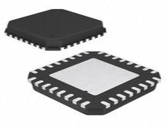
12 Bit 0.5mm Tin ADC AD7490 3V 32-VFQFN Exposed Pad, CSP
Evaluate the AD7490 16-channel ADC for your DAQ system. Review critical SPI timing fixes, digital isolator constraints, power specs, and TI alternatives.
- Overcoming SPI Timing and MISO Isolation Challenges
- Core Specifications and Power Trade-offs
- Leveraging the Channel Sequencer
- Application Mapping: Where the AD7490 Fits
- Alternatives, Equivalents, and Replacement Risk
- Schematic Symbol and PCB Layout Verification
- Frequently Asked Questions
- Specifications
- Parts with Similar Specs
- Datasheet PDF
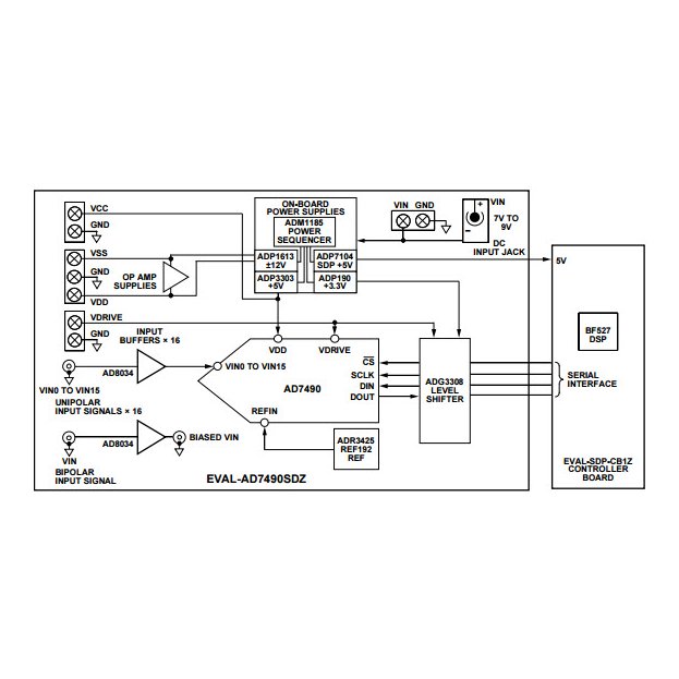
The AD7490 is a 12-bit, 16-channel successive approximation analog-to-digital converter (ADC) designed for high-speed multichannel data acquisition and system monitoring. By combining a 1 MSPS throughput rate with an integrated channel sequencer, it allows microcontrollers to rapidly sweep through multiple sensor inputs with minimal processing overhead.
For design engineers and procurement specialists evaluating this component, the primary value lies in its balance of channel density, speed, and low power consumption. However, successfully integrating the AD7490 requires careful attention to serial interface timing and signal integrity, particularly in isolated environments.
Core Architecture: 12-bit Successive Approximation Register (SAR).
Speed & Density: 1 MSPS throughput across 16 single-ended inputs.
Operating Envelope: 2.7 V to 5.25 V supply, with AEC-Q100 qualification available for automotive use.
Power Efficiency: 5.4 mW maximum at 3 V (870 kSPS), featuring a 0.5 µA full shutdown mode.
Overcoming SPI Timing and MISO Isolation Challenges
The most critical integration hurdles for the AD7490 revolve around its high-speed serial interface. When pushing an ADC to 1 MSPS, the timing margins for the SPI (or QSPI/MICROWIRE/DSP) interface become exceptionally tight. Engineers frequently encounter intermittent BUSY signals or complete readback failures during prototype testing.
These readback errors usually stem from insufficient delay between conversions or poorly tuned SPI clock speeds. At 1 MSPS, the microcontroller must read 16 bits of data (4 dummy/control bits + 12 data bits) within a 1 microsecond window, leaving very little room for propagation delays. If the clock speed is too high, capacitive loading on the lines can cause setup and hold time violations. If the delay between the end of one conversion and the start of the next is too brief, the ADC's internal state machine may not reset properly, triggering a persistent BUSY state. Resolving this requires scoping the SPI lines directly at the component pins to verify that the clock edges align with the datasheet's strict timing diagrams.
A more complex issue arises when the AD7490 is used in systems requiring galvanic isolation, such as industrial power line monitoring or high-voltage battery equipment. Designers often route the SPI bus through digital isolators. However, the MISO (Master In Slave Out) signal from the AD7490 can unexpectedly collapse or severely attenuate when driving certain isolators.
This attenuation is a direct result of line loading or clamping. The internal output driver of the AD7490's serial data out (DOUT) pin has finite drive strength. If the chosen digital isolator has a high input capacitance, a low input impedance, or mismatched clamping diodes, it will load the DOUT net heavily enough to pull the voltage swing below the microcontroller's logic-high threshold.
To mitigate this: 1. Verify Drive Strength: Ensure the selected isolator is explicitly rated for low-current, high-speed SPI operation. 2. Minimize Fanout: Check for multiple isolators or other slave devices loading the same DOUT net. 3. Buffer the Signal: If isolation is strictly required and the signal is collapsing, inserting a small, high-speed logic buffer between the AD7490 DOUT pin and the isolator input can restore signal integrity.
Core Specifications and Power Trade-offs
Evaluating the AD7490 requires understanding the trade-offs between supply voltage, power consumption, and dynamic performance.
The device is specified to operate from a $V_{DD}$ of 2.7 V to 5.25 V. Running the ADC at 5 V provides maximum dynamic range and optimal Signal-to-Noise Ratio (SNR)—specified at 69.5 dB for a 50 kHz input frequency. However, this comes at a power cost. At 5 V and 1 MSPS, the maximum power consumption is 12.5 mW.
If the design is battery-powered, dropping the supply to 3 V significantly improves efficiency, reducing power consumption to a maximum of 5.4 mW. The engineering compromise here is a slight reduction in maximum throughput (down to 870 kSPS at 3 V) and a compressed analog input range, which demands tighter noise control on the PCB layout.
For highly power-sensitive applications, the AD7490 features a full shutdown mode that pulls a maximum of just 0.5 µA. Designers should leverage this state between channel sweeps to dramatically lower the average power profile of the system.
Leveraging the Channel Sequencer
In multichannel system monitoring, MCU overhead is a common bottleneck. The AD7490 includes an internal channel sequencer that allows the ADC to automatically cycle through the 16 single-ended inputs in a pre-programmed order.
Instead of the microcontroller sending a new address prior to every single conversion, the MCU simply clocks out the data as the ADC steps through the sequence. It is important to note that the 1 MSPS throughput is an aggregate figure. If all 16 channels are active in the sequencer, the maximum per-channel sample rate drops to 62.5 kSPS. System architects must size their front-end anti-aliasing filters based on this per-channel sampling rate, not the aggregate 1 MSPS figure.
Application Mapping: Where the AD7490 Fits
The combination of 16 channels and a compact serial interface makes the AD7490 highly specific to certain design architectures:
Data Acquisition (DAQ) and Instrumentation: The wide input bandwidth and high channel count allow a single chip to monitor multiple sensor nodes, reducing BOM count compared to using multiple 4-channel ADCs.
Automotive Applications: With AEC-Q100 qualification, it is suitable for in-cabin or under-hood environmental monitoring where temperature and voltage rails must be constantly swept.
Power Line Monitoring: High-speed sampling captures transient voltage spikes across multiple phases, though this requires the strict isolation design mentioned earlier.
Battery-Powered Equipment: The 0.5 µA shutdown mode and 3 V operation make it viable for portable diagnostic tools.
Alternatives, Equivalents, and Replacement Risk
Procurement teams and designers must always evaluate second-source options or alternative architectures to mitigate supply chain risks. While the AD7490 is a robust part, competitors offer components that may serve as functional equivalents, though rarely as exact drop-in pin-for-pin replacements.
Texas Instruments ADS7952: This is the closest direct competitor in the SAR space. It is a 12-bit, 16-channel ADC with a 1 MSPS throughput. If you are facing sourcing constraints with the AD7490, the ADS7952 is the most logical functional alternative. However, package dimensions, pinouts, and exact SPI control registers will differ, necessitating PCB layout and firmware updates.
Texas Instruments ADS124S08: While sometimes compared in the 16-channel space, this is a radically different architecture. The ADS124S08 is a 24-bit Delta-Sigma ADC. It offers vastly superior resolution but operates at a fraction of the speed (kSPS rather than MSPS). It is only a viable alternative if your design is pivoting away from high-speed transient capture toward ultra-precise, low-speed DC measurements.
Microchip and Maxim Integrated (Analog Devices): Both offer 12-bit multichannel SAR ADCs. When evaluating these, compare the input bandwidth and the power consumption at your specific target logic levels.
Schematic Symbol and PCB Layout Verification
Before releasing a BOM or finalizing a PCB layout utilizing the AD7490, verify the following physical and electrical parameters:
Library Footprint: Confirm the exact package suffix in your EDA tool. The AD7490 is typically available in TSSOP or LFCSP packages. The thermal pad on LFCSP variants must be handled correctly in the footprint to prevent assembly shorts and ensure mechanical stability.
Decoupling: High-speed SAR ADCs require aggressive decoupling. A 10 µF tantalum or ceramic capacitor in parallel with a 0.1 µF ceramic capacitor should be placed as close to the $V_{DD}$ pin as physically possible.
Reference Verification: Because timing tolerances vary by sub-variant and temperature grade, confirming setup and hold times directly in the manufacturer's latest revision documentation is strictly required here to prevent the BUSY state lockups discussed earlier.
Ground Planes: Despite having a serial digital interface, the internal SAR architecture is highly sensitive to noise. Maintain a solid ground plane beneath the ADC, ensuring that high-speed digital return currents from the SPI bus do not cross under the analog input pins.
Frequently Asked Questions
Why does the AD7490 MISO signal collapse when routed through an isolator?The ADC's DOUT pin has limited drive strength. High-capacitance digital isolators or multiple logic gates on the same net can load the line heavily, pulling the signal voltage down. You may need to add a digital buffer between the ADC and the isolator to restore the signal.
Can I replace the AD7490 directly with the Texas Instruments ADS7952?They are functionally similar (both are 12-bit, 16-channel, 1 MSPS SAR ADCs), but they are not exact drop-in replacements. You will need to verify pinout compatibility, package dimensions, and adjust microcontroller firmware to match the specific command registers of the TI part.
How does the channel sequencer impact the 1 MSPS throughput rate?The 1 MSPS rate is the total aggregate throughput of the ADC. If you use the sequencer to sweep across all 16 channels, the maximum sampling rate for each individual channel becomes 1 MSPS divided by 16, or 62.5 kSPS.
What is the minimum power consumption achievable with the AD7490?By dropping the supply voltage to 3 V, active power consumption drops to a maximum of 5.4 mW (at 870 kSPS). When not actively sampling, engaging the full shutdown mode reduces current draw to just 0.5 µA.
Watch Tutorial: AD7490
Specifications
Parts with Similar Specs
- ImagePart NumberManufacturerPackage / CaseNumber of PinsNumber of BitsSampling RatePolarityInterfaceIntegral Nonlinearity (INL)Differential NonlinearityNumber of A/D ConvertersMin Supply VoltageSupply VoltageView Compare
![AD7490BCPZ-REEL7]()
AD7490BCPZ-REEL7
32-VFQFN Exposed Pad, CSP
32
12
150 ksps
Unipolar
SPI
1 LSB
-0.95 LSB
1
2.7 V
3 V
![AD7877ACPZ-500RL7]()
32-VFQFN Exposed Pad, CSP
32
12
1 Msps
Unipolar
SPI
1.5 LSB
-0.99 LSB
-
2.7 V
3 V
![AD7265BCPZ]()
32-VFQFN Exposed Pad, CSP
32
12
1 Msps
Unipolar
SPI
1.5 LSB
-0.99 LSB
-
2.7 V
3 V
![AD7265BCPZ-REEL7]()
32-VFQFN Exposed Pad, CSP
32
12
125 ksps
-
SPI
2 LSB
-
1
-
-

Datasheet PDF
- Datasheets :
- PCN Design/Specification :
- ConflictMineralStatement :
 xc6220b331mr-g:LDO Voltage Regulators 1A High Speed Green Operation Vltg Reg
03 March 20221265
 TL082 JFET-Input Dual Operational Amplifier: Datasheet Breakdown and Design Guide
20 January 2026246
 HC-06 vs. HC-05 Bluetooth Module: What is the difference between HC-06 and HC-05?
24 November 202161081
 Comprehensive Guide to XC7Z010-1CLG400C Specifications and Features
21 February 20251048
 A Comprehensive Guide to LTC691CSW#TRPBF PMIC Supervisors
06 March 2024193
 PIC16F688 Microcontroller by Microchip Technology: Detailed Technical Analysis
29 February 2024142
 STMPS2151STR Switch: Features, Applications and Datasheet
22 November 2023353
 ATMEGA16U2-MU 8-Bit Microcontroller: Features, Pinout, and Datasheet
12 February 20225633
 Millimeter Wave Radar: Advantages, Types, and Applications
18 October 202119744
 nF Capacitors: Definition, Conversion, Circuit Applications, and Selection
12 August 20256577
 Top Picks for Circuit Breakers This Year
10 July 20255600
 Understanding the Crystal Oscillator: Construction, Working Principles and Applications
08 July 20243781
 Silicon Carbide Semiconductor Devices at Ultra-high Voltages and their Applications
04 January 20231962
 What is LCD? Working Principle, Features, and Future Trends
05 January 202613173
 The Future of Automated and Additive Manufacturing for Power Electronics
24 May 20233397
 What is a Ground Fault Circuit Interrupter?
27 March 20255252
Analog Devices Inc.
In Stock: 6000
United States
China
Canada
Japan
Russia
Germany
United Kingdom
Singapore
Italy
Hong Kong(China)
Taiwan(China)
France
Korea
Mexico
Netherlands
Malaysia
Austria
Spain
Switzerland
Poland
Thailand
Vietnam
India
United Arab Emirates
Afghanistan
Åland Islands
Albania
Algeria
American Samoa
Andorra
Angola
Anguilla
Antigua & Barbuda
Argentina
Armenia
Aruba
Australia
Azerbaijan
Bahamas
Bahrain
Bangladesh
Barbados
Belarus
Belgium
Belize
Benin
Bermuda
Bhutan
Bolivia
Bonaire, Sint Eustatius and Saba
Bosnia & Herzegovina
Botswana
Brazil
British Indian Ocean Territory
British Virgin Islands
Brunei
Bulgaria
Burkina Faso
Burundi
Cabo Verde
Cambodia
Cameroon
Cayman Islands
Central African Republic
Chad
Chile
Christmas Island
Cocos (Keeling) Islands
Colombia
Comoros
Congo
Congo (DRC)
Cook Islands
Costa Rica
Côte d’Ivoire
Croatia
Cuba
Curaçao
Cyprus
Czechia
Denmark
Djibouti
Dominica
Dominican Republic
Ecuador
Egypt
El Salvador
Equatorial Guinea
Eritrea
Estonia
Eswatini
Ethiopia
Falkland Islands
Faroe Islands
Fiji
Finland
French Guiana
French Polynesia
Gabon
Gambia
Georgia
Ghana
Gibraltar
Greece
Greenland
Grenada
Guadeloupe
Guam
Guatemala
Guernsey
Guinea
Guinea-Bissau
Guyana
Haiti
Honduras
Hungary
Iceland
Indonesia
Iran
Iraq
Ireland
Isle of Man
Israel
Jamaica
Jersey
Jordan
Kazakhstan
Kenya
Kiribati
Kosovo
Kuwait
Kyrgyzstan
Laos
Latvia
Lebanon
Lesotho
Liberia
Libya
Liechtenstein
Lithuania
Luxembourg
Macao(China)
Madagascar
Malawi
Maldives
Mali
Malta
Marshall Islands
Martinique
Mauritania
Mauritius
Mayotte
Micronesia
Moldova
Monaco
Mongolia
Montenegro
Montserrat
Morocco
Mozambique
Myanmar
Namibia
Nauru
Nepal
New Caledonia
New Zealand
Nicaragua
Niger
Nigeria
Niue
Norfolk Island
North Korea
North Macedonia
Northern Mariana Islands
Norway
Oman
Pakistan
Palau
Palestinian Authority
Panama
Papua New Guinea
Paraguay
Peru
Philippines
Pitcairn Islands
Portugal
Puerto Rico
Qatar
Réunion
Romania
Rwanda
Samoa
San Marino
São Tomé & Príncipe
Saudi Arabia
Senegal
Serbia
Seychelles
Sierra Leone
Sint Maarten
Slovakia
Slovenia
Solomon Islands
Somalia
South Africa
South Sudan
Sri Lanka
St Helena, Ascension, Tristan da Cunha
St. Barthélemy
St. Kitts & Nevis
St. Lucia
St. Martin
St. Pierre & Miquelon
St. Vincent & Grenadines
Sudan
Suriname
Svalbard & Jan Mayen
Sweden
Syria
Tajikistan
Tanzania
Timor-Leste
Togo
Tokelau
Tonga
Trinidad & Tobago
Tunisia
Turkey
Turkmenistan
Turks & Caicos Islands
Tuvalu
U.S. Outlying Islands
U.S. Virgin Islands
Uganda
Ukraine
Uruguay
Uzbekistan
Vanuatu
Vatican City
Venezuela
Wallis & Futuna
Yemen
Zambia
Zimbabwe
![ADV7513BSWZ]() ADV7513BSWZ
ADV7513BSWZAnalog Devices, Inc.
![AD9877ABSZ]() AD9877ABSZ
AD9877ABSZAnalog Devices, Inc.
![LTC2245CUH#TRPBF]() LTC2245CUH#TRPBF
LTC2245CUH#TRPBFLinear Technology/Analog Devices
![AD7791BRMZ-REEL]() AD7791BRMZ-REEL
AD7791BRMZ-REELAnalog Devices Inc.
![AD7799BRUZ-REEL]() AD7799BRUZ-REEL
AD7799BRUZ-REELAnalog Devices Inc.
![AD7190BRUZ-REEL]() AD7190BRUZ-REEL
AD7190BRUZ-REELAnalog Devices Inc.
![AD7705BRZ-REEL]() AD7705BRZ-REEL
AD7705BRZ-REELAnalog Devices Inc.
![AD7175-2BRUZ-RL7]() AD7175-2BRUZ-RL7
AD7175-2BRUZ-RL7Analog Devices Inc.
![AD7192BRUZ-REEL]() AD7192BRUZ-REEL
AD7192BRUZ-REELAnalog Devices Inc.
![AD9283BRSZ-RL100]() AD9283BRSZ-RL100
AD9283BRSZ-RL100Analog Devices Inc.


