The Future of Automated and Additive Manufacturing for Power Electronics
| Topics covered in this article: |
| Ⅰ. Drawbacks of Additive Manufacturing Technology |
| Ⅱ. The Future of Automated and Additive Manufacturing |
| Ⅲ. Summarizing the Key Points |
| Ⅳ. Reference(s) |
A full power electronics converter has not yet been created utilizing only additive manufacturing (AM) technology. It might still be necessary to build each component of the power electronics converters independently, followed by assembling them. It makes sense to use several additive manufacturing technologies for various sorts of components because each one has advantages of its own. However, the manufacture of capacitors and resistors for converters that operate at high voltages and frequencies has long relied on traditional processing techniques.
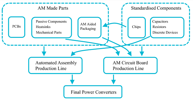
Figure 1. Potential future automated manufacturing processes combined with additive manufacturing for power electronics converters. As the arrow shows, previously fabricated components will be delivered in the direction shown. Image used courtesy of IEEE Journal of Emerging and Selected Topics in Power Electronics
The advancement of autonomous manufacturing technology (AMFG) makes it possible to fully automate the assembly procedure. Figure 1 depicts the potential benefits of combining automated manufacturing and additive manufacturing techniques with conventional parts that have been standardized and modularized. The manufacturing procedures in Figure 1 are designed to make the best use of additive manufacturing.
Ⅰ. Drawbacks of Additive Manufacturing Technology
Traditional manufacturing techniques continue to be the most economical and dependable choice for some inverters, such as high-volume inverters with simple structures. Table 1 displays the advantages and disadvantages of additive manufacturing. It suggests that the fundamental drawback of additive manufacturing is its inferior material characteristics. This is the main issue preventing the use of additive manufacturing in power electronics. However, with the advancement of additive manufacturing and compensating measures, this issue is gradually being solved.
Table 1. Advantages and disadvantages of using additive manufacturing for each part
Advantages | Disadvantages | |
Passive Parts | Geometrical flexibility to help minimize winding losses, Precisely duplicate the designed winding dimension to control the component parameters. | low electric conductivity; Bad high-frequency performance. |
Electric Circuits | Free and multilayer layout; easily embedding components, reduction in waste. | low conductivity of conducting traces; High price. |
Thermal Management and Packaging | Geometrically free to make complex and compact structures with high thermal performance, forming non-metal coolers with inner cooling channels, new packaging forms. | low thermal conductivity without post-treatment. |
The electrical conductivity of PCBs from Nano Dimension has improved from 5% to 30% of the international annealed copper standard (IACS) to 25% to 50% of the IACS. 50% IACS is a close match to the standard PCB conductivity of 86% IACS. Due to the fact that doubling the size of the conductive traces is an effective method since it will not increase the board's surface area, postprint heat treatment could also enhance the thermal conductivity of additively manufactured alloys.
In addition to the material concerns, the following list includes some more restrictions on additive manufacturing technology in power electronics.
l Lacking specialized software and tools for computation.
l Low throughput and high costs are associated with mass production.
l Reliability of the production process and the final products.
l Resolution and printing speed are trade-offs.
Lacking specialized software and tools for computation
A critical problem that needs to be solved is a lack of specialized software. Currently, CAD/CAM software is used to develop additive manufacturing components. However, the software does not take into account new design guidelines or analysis techniques. In the near future, Nano Dimension intends to release AM PCB design and verification tools. With the help of this program, it is possible to create 3-D PCBs as well as 3-D electrical components while integrating conventional CAD tools, enabling smooth design-to-print processes. With the promotion of additive manufacturing technology, it is thought that the software problem could be resolved.
Low throughput and high costs are associated with mass production
Additionally, compared to conventional ones, the price of power electronics converters that use additive manufacturing is relatively high. If this issue cannot be solved, then additive manufacturing technology will only be used for one-off or low-volume power electronics converter production.
Reliability of the production process and the final products
The reliability of the procedure is a big additional challenge. Due to the complexity of the majority of components created for additive manufacturing, it can occasionally be challenging to properly produce a unique design using only one-shot work. It is required to alter process configurations regularly to obtain perfect outcomes. This procedure limits rapid prototyping fulfillment because it takes a lot of time and resources.
High-resolution printing also leads to thinner printing layers and smaller feature sizes in the planar direction, which prolongs building durations and increases the possibility of errors. The surface roughness of printed components is typically worse than that of traditional components.
For conductive traces, for instance, the surface roughness value Sa is typically less than 2 μm. The Savalue of a printed copper winding, however, can be as high as 20 μm as built and as low as 8.3 μm after postetching. A heat sink that has been ground has a roughness of around 2 μm (Rq value), but a heat sink that has been 3-D printed has a roughness of about 10 μm. A rough surface has an adverse effect on the assembly surface and increases the surface area and heat exchange coefficient.
Resolution and printing speed are trade-offs
Under typical conditions, additive manufacturing does not always result in faster processing times than conventional techniques. The anticipated construction times for additive manufacturing and conventional techniques are contrasted in Table 2. The intricacy of the parts and the component size both have an impact on how long it takes to construct a part using additive manufacturing, but this effect is far less pronounced than it would be with traditional manufacturing techniques.
Table 2: Comparison of estimated build times between additive manufacturing and conventional processes
AM Time | Process | Time | |
PCB | 40-100 hours for a 160 mm x 160 mm area | From finishing data preparation to completing production |
1-30 days |
Heatsink | 3-50 hours | Extrusion
Casting
CNC machining | 3-10 mins/one billet
1-7 mins
2-5 hours |
According to the Nano Dimension procedure for 3-D printed PCBs, if the board's size is small, numerous boards can be manufactured simultaneously in the 160 mm x 160 mm region, reducing the construction time for each board proportionately. The PCB's structure and layer count have a significant impact on how quickly it can be processed in conventional manufacturing. When producing a multilayer PCB or a particular structural board, such as a PCB with countersink holes, suppliers always demand a significantly longer lead time.
It should be emphasized that the extruding procedure is the most time-efficient way to make fin-type heat sinks. Many heat sinks can be produced from one rod. Processes including preheating, straightening, and aging take many extra hours before and after extrusion. For big volume production, the average processing time for a heat sink is generally quite brief.
However, since additive manufacturing or CNC machining does not need specially manufactured molds, which typically take 7 to 30 days, they are preferable options for customized heat sinks with unique architectures and lower production volumes. For the additive manufacturing process, only one piece of equipment is needed. In contrast to creating a production line, this technique can be carried out in a lab or by a company in the area.
Making a heat sink that is liquid-cooled and has internal flow channels, for example, is possible with additive manufacturing almost without geometry restrictions. From this point of view, it makes perfect sense to classify additive manufacturing as a rapid prototyping technology. Because 3-D printed items have rougher surfaces than machined parts do, the machining process must still be used to assure precision, which adds additional time for particular holes or surfaces with assembly requirements.
Ⅱ. The Future of Automated and Additive Manufacturing
Other than what has already been described, the key research focus for power electronics converter manufacturing will be combining design automation, additive manufacturing, and automated manufacturing. PowerSynth and ParaPower are only two examples of the many design tools that are currently becoming more advanced and interconnected. An electro-thermo-mechanical design environment might be created using these two technologies in conjunction with an application programming interface, enabling the simultaneous design and optimization of power modules.
The analysis of electrical, magnetic, thermal, and mechanical data in accordance with the necessary operating parameters and material qualities will enable electronic design automation tools to get smarter as technology develops and automatically finish the design of entire power electronics converters. The AMFG Company made public the autonomous manufacturing platform, which can also offer a full end-to-end integrated management system for additive manufacturing.
It can provide automatic administration for additive manufacturing processes such as machine monitoring, production scheduling, and quality management. It can automatically evaluate 3-D printability and convert files output from design software to additive manufacturing format. This enables an autonomous additive manufacturing process. Future power electronics converter design and production may be able to be completed with a single click, leading to an increase in the number of customized products.
Ⅲ. Summarizing the Key Points
l Additive manufacturing technology has the potential to revolutionize the production of power electronics converters, but a full power electronics converter has not yet been created using only this technology.
l Different additive manufacturing technologies can be used for various components of power electronics, each with its own advantages and limitations.
l The advancement of autonomous manufacturing technology makes it possible to fully automate the assembly procedure, which can lead to potential benefits.
l Traditional processing techniques continue to be the most economical and dependable choice for some inverters, such as high-volume inverters with simple structures.
l While there are still challenges associated with using additive manufacturing technology, such as a lack of specialized software and tools for computation, low throughput, and high costs associated with mass production,
l Continued research and development in this additive manufacturing technology could lead to significant advancements in the field of power electronics.
Ⅳ. Reference(s)
Zhang, Z., & Yuan, X. (2022, August). Applications and Future of Automated and Additive Manufacturing for Power Electronics Components and Converters. IEEE Journal of Emerging and Selected Topics in Power Electronics, 10(4), 4509–4525. https://doi.org/10.1109/jestpe.2021.3135285
 Improving the Energy Conversion Efficiency of Triboelectric NanogeneratorsSaumitra Jagdale19 November 20242591
There is a huge growth in demand for self-sustaining electronic devices, as the traditional power-generating devices fail in remote and harsh environments due to the periodic requirement of battery changes. Also, these devices are frequency specific; some work only in high frequency and some in low frequency. Triboelectric nanogenerators (TENGs) provide a promising solution by efficiently converting mechanical energy into electricity as they are versatile, compact, and cheap, making them a popular choice.
Read More Methodologies for Increasing Efficiency of Fuel Stack Technology for Energy GenerationSaumitra Jagdale19 November 20242602
Presently, power companies are moving towards renewable energy systems. Conventional energy sources are more expensive because they require a vast network to be maintained and huge human resources. Also, they harm the environment by releasing several harmful gases. As the industry’s focus shifts toward renewable energy sources, energy systems powered by Proton Exchange Membrane Fuel Stacks (PEMFS) are gaining traction.
Read More Reconfigurable Antennas: Improving Efficiency in Modern CommunicationRakesh Kumar, Ph.D.24 December 20242542
This article highlights the limitations of conventional antennas and discusses the advantages of reconfigurable antenna designs. It also explores various reconfiguration techniques, applications, and their potential to enhance efficiency.
Read More The Ultimate Guide to AI Noise Reduction Translation EarbudsUTMEL01 April 20256886
In today’s connected world, talking to others is very important. You’ve likely seen how global business, travel, and learning need easy chats in different languages. This need keeps growing because of new tech like 5G and edge computing. These make fast and smooth connections possible.
Read More Comparing Popular Jumper Wires for Electronics ProjectsUTMEL10 July 20251702
Compare top jumper wires for electronics projects in 2025. Explore options by material, length, gauge, and durability to find the best fit for your needs.
Read More
Subscribe to Utmel !


 Product
 Brand
Brand Articles
 Tools
Tools


