
 Product
 Brand
Brand Articles
 Tools
Tools
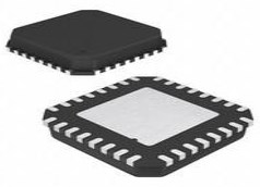
xc6220b331mr-g:LDO Voltage Regulators 1A High Speed Green Operation Vltg Reg


Enable Fixed XC6220 PMIC SC-74A, SOT-753
xc6220b331mr-g is a kind of voltage regulator with a Green Operation function. This passage is going to introduce xc6220b331mr-g in the perspectives of description, features, and pinout.
xc6220b331mr-g description
The XC6220 series is a CMOS voltage regulator with Green Operation that is highly accurate, low noise, fast, has a low dropout, and has a large current. A voltage reference, an error amplifier, a current limiter, an inrush current prevention circuit, a phase compensation circuit, and a driver transistor are all part of the series.
The ultra-low dropout voltage performance with output currents up to 1A with a 0.2 on-resistance driver transistor integrated greatly extends battery life, as does the Green Operation function, which can switch between high speed and power save modes automatically. For the output stabilization capacitor, a low ESR ceramic capacitor can be used (CL).
Using laser trimming technologies, the output voltage can be adjusted in 0.05V increments within a range of 0.8V5.0V. There is an overcurrent protection circuit as well as a thermal shutdown circuit built-in. When the output current reaches its limit current, the over-current protection circuit kicks in. When the junction temperature reaches its limit temperature, the thermal shutdown circuit will activate. The inrush prevention circuit controls the inrush current that charges to CL when the IC starts up. Voltage fluctuations in the power supply caused by inrush current during system startup can thus be reduced.
The CE function allows the output to be disabled and the IC to enter a standby mode, resulting in significantly reduced power consumption.
xc6220b331mr-g application
Optical disk drive
Magnetic disk drive
UMPCs
Digital still cameras / Camcorders
Digital audio equipment
CD-ROM, CD-R/RW drives
DVD drives
HDD drives
MIDs, Video cameras
Portable AV equipment
xc6220b331mr-g features
Maximum Output Current Dropout Voltage Operating Voltage Range Output Voltage Range Accuracy Low Power Consumption Operating Temperature Thermal Shutdown Inrush Current Protection CL Auto Discharge CE Pull-Down Resistor Output Capacitor Packages Environmentally Friendly 1000mA (TYP.:1200mA limit) 5.0V (0.05V increments): 8A (TYP.) in PS mode: 50A (TYP.) in HS mode Detect 150, Release: 700mA (MAX.): XC6220B/D Series: XC6220C/D Series: Ceramic Capacitor Compatible: EU RoHS Compliant, Pb Free
* The No.5 and 6 VIN pins should be connected. The No.1 and 2 pins VOUT pins should be connected. The dissipation pad for the USP-6C package should be solder-plated in recommended mount pattern and metal masking to enhance mounting strength and heat release. If the pad needs to be connected to other pins, it should be connected to the VSS (No. 4)
SOT-25 PIN NUMBER SOT-89-5 USP-6C PIN NAME CE VIN VSS VOUT NC FUNCTIONS ON/OFF Control Power Input Ground Output No connection
Selection Guide Please see the optional setting for CL discharge and internal CE pull-down. PRODUCT NAME XC6220C XC6220D CONDITIONS without CE Pull-down resistor, without CL auto discharge (Semi-custom) without CE Pull-down resistor, with CL auto discharge (Standard) with CE Pull-down resistor, without CL auto discharge (Semi-custom) with CE Pull-down resistor, with CL auto discharge (Semi-custom).
xc6220b331mr-g CAD models
symbol

footprint

3D


Specifications
- TypeParameter
- Factory Lead Time10 Weeks
- Mount
In electronic components, the term "Mount" typically refers to the method or process of physically attaching or fixing a component onto a circuit board or other electronic device. This can involve soldering, adhesive bonding, or other techniques to secure the component in place. The mounting process is crucial for ensuring proper electrical connections and mechanical stability within the electronic system. Different components may have specific mounting requirements based on their size, shape, and function, and manufacturers provide guidelines for proper mounting procedures to ensure optimal performance and reliability of the electronic device.
Surface Mount - Mounting Type
The "Mounting Type" in electronic components refers to the method used to attach or connect a component to a circuit board or other substrate, such as through-hole, surface-mount, or panel mount.
Surface Mount - Package / Case
refers to the protective housing that encases an electronic component, providing mechanical support, electrical connections, and thermal management.
SC-74A, SOT-753 - Number of Pins5
- Usage LevelIndustrial grade
- Operating Temperature
The operating temperature is the range of ambient temperature within which a power supply, or any other electrical equipment, operate in. This ranges from a minimum operating temperature, to a peak or maximum operating temperature, outside which, the power supply may fail.
-40°C~85°C - Packaging
Semiconductor package is a carrier / shell used to contain and cover one or more semiconductor components or integrated circuits. The material of the shell can be metal, plastic, glass or ceramic.
Tape & Reel (TR) - Published2009
- JESD-609 Code
The "JESD-609 Code" in electronic components refers to a standardized marking code that indicates the lead-free solder composition and finish of electronic components for compliance with environmental regulations.
e3 - Part Status
Parts can have many statuses as they progress through the configuration, analysis, review, and approval stages.
Active - Moisture Sensitivity Level (MSL)
Moisture Sensitivity Level (MSL) is a standardized rating that indicates the susceptibility of electronic components, particularly semiconductors, to moisture-induced damage during storage and the soldering process, defining the allowable exposure time to ambient conditions before they require special handling or baking to prevent failures
1 (Unlimited) - Number of Terminations5
- ECCN Code
An ECCN (Export Control Classification Number) is an alphanumeric code used by the U.S. Bureau of Industry and Security to identify and categorize electronic components and other dual-use items that may require an export license based on their technical characteristics and potential for military use.
EAR99 - Terminal Finish
Terminal Finish refers to the surface treatment applied to the terminals or leads of electronic components to enhance their performance and longevity. It can improve solderability, corrosion resistance, and overall reliability of the connection in electronic assemblies. Common finishes include nickel, gold, and tin, each possessing distinct properties suitable for various applications. The choice of terminal finish can significantly impact the durability and effectiveness of electronic devices.
Tin (Sn) - Terminal Position
In electronic components, the term "Terminal Position" refers to the physical location of the connection points on the component where external electrical connections can be made. These connection points, known as terminals, are typically used to attach wires, leads, or other components to the main body of the electronic component. The terminal position is important for ensuring proper connectivity and functionality of the component within a circuit. It is often specified in technical datasheets or component specifications to help designers and engineers understand how to properly integrate the component into their circuit designs.
DUAL - Terminal Form
Occurring at or forming the end of a series, succession, or the like; closing; concluding.
GULL WING - Peak Reflow Temperature (Cel)
Peak Reflow Temperature (Cel) is a parameter that specifies the maximum temperature at which an electronic component can be exposed during the reflow soldering process. Reflow soldering is a common method used to attach electronic components to a circuit board. The Peak Reflow Temperature is crucial because it ensures that the component is not damaged or degraded during the soldering process. Exceeding the specified Peak Reflow Temperature can lead to issues such as component failure, reduced performance, or even permanent damage to the component. It is important for manufacturers and assemblers to adhere to the recommended Peak Reflow Temperature to ensure the reliability and functionality of the electronic components.
260 - Number of Functions1
- Time@Peak Reflow Temperature-Max (s)
Time@Peak Reflow Temperature-Max (s) refers to the maximum duration that an electronic component can be exposed to the peak reflow temperature during the soldering process, which is crucial for ensuring reliable solder joint formation without damaging the component.
10 - Base Part Number
The "Base Part Number" (BPN) in electronic components serves a similar purpose to the "Base Product Number." It refers to the primary identifier for a component that captures the essential characteristics shared by a group of similar components. The BPN provides a fundamental way to reference a family or series of components without specifying all the variations and specific details.
XC6220 - Current - Supply (Max)
The parameter "Current - Supply (Max)" in electronic components refers to the maximum amount of current that a component can draw from a power supply for its operation. This parameter is critical for ensuring that the power supply can adequately meet the demands of the component without causing damage or malfunction. Exceeding this specified maximum current can lead to overheating, reduced performance, or failure of the component. It is essential to consider this value when designing or integrating components into electronic circuits to maintain reliability and functionality.
108μA - Voltage - Input (Max)
Voltage - Input (Max) is a parameter in electronic components that specifies the maximum voltage that can be safely applied to the input of the component without causing damage. This parameter is crucial for ensuring the proper functioning and longevity of the component. Exceeding the maximum input voltage can lead to electrical overstress, which may result in permanent damage or failure of the component. It is important to carefully adhere to the specified maximum input voltage to prevent any potential issues and maintain the reliability of the electronic system.
6V - Output Voltage
Output voltage is a crucial parameter in electronic components that refers to the voltage level produced by the component as a result of its operation. It represents the electrical potential difference between the output terminal of the component and a reference point, typically ground. The output voltage is a key factor in determining the performance and functionality of the component, as it dictates the level of voltage that will be delivered to the connected circuit or load. It is often specified in datasheets and technical specifications to ensure compatibility and proper functioning within a given system.
3.3V - Output Type
The "Output Type" parameter in electronic components refers to the type of signal or data that is produced by the component as an output. This parameter specifies the nature of the output signal, such as analog or digital, and can also include details about the voltage levels, current levels, frequency, and other characteristics of the output signal. Understanding the output type of a component is crucial for ensuring compatibility with other components in a circuit or system, as well as for determining how the output signal can be utilized or processed further. In summary, the output type parameter provides essential information about the nature of the signal that is generated by the electronic component as its output.
Fixed - Output Configuration
Output Configuration in electronic components refers to the arrangement or setup of the output pins or terminals of a device. It defines how the output signals are structured and how they interact with external circuits or devices. The output configuration can determine the functionality and compatibility of the component in a circuit design. Common types of output configurations include single-ended, differential, open-drain, and push-pull configurations, each serving different purposes and applications in electronic systems. Understanding the output configuration of a component is crucial for proper integration and operation within a circuit.
Positive - Control Features
Control features in electronic components refer to specific functionalities or characteristics that allow users to manage and regulate the operation of the component. These features are designed to provide users with control over various aspects of the component's performance, such as adjusting settings, monitoring parameters, or enabling specific modes of operation. Control features can include options for input/output configurations, power management, communication protocols, and other settings that help users customize and optimize the component's behavior according to their requirements. Overall, control features play a crucial role in enhancing the flexibility, usability, and performance of electronic components in various applications.
Enable - Output Voltage 1
Output Voltage 1 is a parameter commonly found in electronic components such as voltage regulators, power supplies, and amplifiers. It refers to the voltage level that is produced or delivered by the component at a specific output terminal or pin. This parameter is crucial for determining the performance and functionality of the component in a circuit. The specified output voltage should meet the requirements of the connected devices or components to ensure proper operation and compatibility. It is important to carefully consider and verify the output voltage 1 specification when selecting and using electronic components in a design or application.
3.3V - Number of Regulators
A regulator is a mechanism or device that controls something such as pressure, temperature, or fluid flow. The voltage regulator keeps the power level stabilized. A regulator is a mechanism or device that controls something such as pressure, temperature, or fluid flow.
1 - Min Input Voltage
The parameter "Min Input Voltage" in electronic components refers to the minimum voltage level that must be applied to the component for it to operate within its specified parameters. This value is crucial as providing a voltage below this minimum threshold may result in the component malfunctioning or not functioning at all. It is important to adhere to the specified minimum input voltage to ensure the proper operation and longevity of the electronic component. Failure to meet this requirement may lead to potential damage to the component or the overall system in which it is used.
1.6V - Protection Features
Protection features in electronic components refer to the built-in mechanisms or functionalities designed to safeguard the component and the overall system from various external factors or internal faults. These features are crucial for ensuring the reliability, longevity, and safety of the electronic device. Common protection features include overvoltage protection, overcurrent protection, reverse polarity protection, thermal protection, and short-circuit protection. By activating these features when necessary, the electronic component can prevent damage, malfunctions, or hazards that may arise from abnormal operating conditions or unforeseen events. Overall, protection features play a vital role in enhancing the robustness and resilience of electronic components in diverse applications.
Over Current, Over Temperature - Current - Quiescent (Iq)
The parameter "Current - Quiescent (Iq)" in electronic components refers to the amount of current consumed by a device when it is in a quiescent or idle state, meaning when it is not actively performing any tasks or operations. This parameter is important because it represents the baseline power consumption of the device even when it is not actively being used. A lower quiescent current (Iq) value is desirable as it indicates that the device is more energy-efficient and will consume less power when not in use, which can help extend battery life in portable devices and reduce overall power consumption in electronic systems. Designers often pay close attention to the quiescent current specification when selecting components for low-power applications or battery-operated devices.
18μA - Voltage Dropout (Max)
Voltage Dropout (Max) refers to the minimum voltage difference between the input and output of a voltage regulator or linear power supply needed to maintain proper regulation. It indicates the maximum allowable voltage drop across the device for it to function effectively without dropout. If the input voltage falls below this threshold, the output voltage may drop below the specified level, leading to potential operational issues for connected components. This parameter is critical for ensuring stable and reliable power delivery in electronic circuits.
0.655V @ 1A - PSRR
PSRR stands for Power Supply Rejection Ratio. It is a measure of how well a device, such as an amplifier or a voltage regulator, can reject variations in the power supply voltage. A high PSRR value indicates that the device is able to maintain its performance even when the power supply voltage fluctuates. This parameter is important in ensuring stable and reliable operation of electronic components, especially in applications where the power supply voltage may not be perfectly regulated. A good PSRR helps to minimize noise and interference in the output signal of the device.
50dB (1kHz) - Dropout Voltage
Dropout voltage is the input-to-output differential voltage at which the circuit ceases to regulate against further reductions in input voltage; this point occurs when the input voltage approaches the output voltage.
655mV - Min Current Limit
Min Current Limit is a parameter in electronic components that refers to the minimum amount of current that must flow through the component to ensure proper operation. This parameter is important because if the current falls below this limit, the component may not function as intended or may even be damaged. Manufacturers specify the minimum current limit to help users understand the operating conditions and limitations of the component. It is crucial to ensure that the current flowing through the component remains above the specified minimum limit to maintain its performance and reliability.
1.005A - Nominal Output Voltage
Nominal Output Voltage refers to the specified or intended voltage level that an electronic component or device is designed to provide as output under normal operating conditions. It is a crucial parameter that indicates the expected voltage level that the component will deliver to the connected circuit or load. This value is typically specified by the manufacturer and is important for ensuring proper functionality and compatibility within a system. It is important to note that the actual output voltage may vary slightly due to factors such as load variations, temperature changes, and other environmental conditions.
3.3V - Length2.9mm
- REACH SVHC
The parameter "REACH SVHC" in electronic components refers to the compliance with the Registration, Evaluation, Authorization, and Restriction of Chemicals (REACH) regulation regarding Substances of Very High Concern (SVHC). SVHCs are substances that may have serious effects on human health or the environment, and their use is regulated under REACH to ensure their safe handling and minimize their impact.Manufacturers of electronic components need to declare if their products contain any SVHCs above a certain threshold concentration and provide information on the safe use of these substances. This information allows customers to make informed decisions about the potential risks associated with using the components and take appropriate measures to mitigate any hazards.Ensuring compliance with REACH SVHC requirements is essential for electronics manufacturers to meet regulatory standards, protect human health and the environment, and maintain transparency in their supply chain. It also demonstrates a commitment to sustainability and responsible manufacturing practices in the electronics industry.
No SVHC - RoHS Status
RoHS means “Restriction of Certain Hazardous Substances” in the “Hazardous Substances Directive” in electrical and electronic equipment.
ROHS3 Compliant
Trend Analysis
Datasheet PDF
- Datasheets :
- Environmental Information :
Parts with Similar Specs
xc6220b331mr-g package
| PACKAGE | OUTLINE / LAND PATTERN | THERMAL CHARACTERISTICS | |
| SOT-25 | SOT-25 PKG | Standard Board | SOT-25 Power Dissipation |
| JESD51-7 Board | |||
| SOT-89-5 | SOT-89-5 PKG | Standard Board | SOT-89-5 Power Dissipation |
| JESD51-7 Board | |||
| USP-6C | USP-6C PKG | Standard Board | USP-6C Power Dissipation |
| JESD51-7 Board | |||
| SOP-8FD | SOP-8FD PKG | Standard Board | SOP-8FD Power Dissipation |
| JESD51-7 Board | |||
xc6220b331mr-g manufacturer
Torex is a leading provider of CMOS power management ICs targeted toward battery-powered and energy-efficient applications. Torex specializes in CMOS analog technology, with LDO voltage regulators, voltage detectors, and DC/DC converters making up their core product offering. Using laser trimming, they are able to offer 1% and 2% accuracy devices. Many of their devices are available in 0.05V increments.
Additional Torex products include charge pump ICs, Multi-Chip Modules, Mosfets, op-amps, oscillators, PLL clock generator ICs, Schottky barrier diodes, battery charger ICs, Hall Effect ICs, and load switches. Torex offers a unique GO "Green Operation" energy-saving function. Many of their devices are able to automatically or manually switch between high-speed mode and power save mode depending upon the load current. Torex offers some of the smallest packages in the world. All of their devices are RoHS compliant, and their complete product line-up will also be halogen and antimony free by 2Q 2010.
What is xc6220b331mr-g?
It is a kind of voltage regulator with a Green Operation function.
What’s the advantages of xc6220b331mr-g?
It is highly accurate, has low noise, high speed, low dropout, and large current.
What should we notice when we use xc6220b331mr-g?
1. For temporary, transitional voltage drop or voltage rising phenomenon, the IC is liable to malfunction should the ratings be exceeded.
2. Where wiring impedance is high, operations may become unstable due to noise and/or phase lag depending on the output current. Please strengthen VIN and VSS wiring in particular.
3. Please wire the input capacitor (CIN) and the output capacitor (CL) as close to the IC as possible.
4. As for the XC6220A/C series (semi-custom), the output voltage may float with a leakage current of the driver transistor between VIN and VOUT and R1+R2 resistance while stand-by (operation stop). Please take consideration of this and check it
before use.
How many pins does xc6220b331mr-g have?and what are they?
It has 5 pins. They are VOUT, NC, VIN, VSS, and CE.
Where can we see xc6220b331mr-g in our daily life?
We can see it in many places. It contains cameras, DVDs and other audio equipment.
 LTC6990IDCB#TRPBF - Programmable Timer and Oscillator for Precision Timing Applications
06 March 2024228
 Unveiling the Texas Instruments MSP430F20x Microcontroller Series: A Comprehensive Analysis
29 February 2024190
 ATTINY26L-8MU 8-bit Microcontroller: Pinout, Equivalent and Datasheet
28 March 2022973
 Cypress CY8C6247BZI-D34 Microcontroller Datasheet Overview
28 February 2024157
![Everything you know about TCS34725 Color Sensors [FAQ]](https://res.utmel.com/Images/Article/8b21ce05-e0d5-4531-9ab0-b9ef621331e0.jpg) Everything you know about TCS34725 Color Sensors [FAQ]
Everything you know about TCS34725 Color Sensors [FAQ]25 April 20229932
![KA7500B Controller: Features, Pinout, and Datasheet [Video&FAQ]](https://res.utmel.com/Images/Article/f00ffbff-eb5d-4a0c-90bf-75484b9ef533.png) KA7500B Controller: Features, Pinout, and Datasheet [Video&FAQ]
KA7500B Controller: Features, Pinout, and Datasheet [Video&FAQ]21 October 202157623
![SS16 DIODE Schottky Rectifier 60 V 1 A SMA[FAQ]: Datasheet, Features, and Applications](https://res.utmel.com/Images/Article/f131989f-5eb8-4b31-b322-a99c4cdff30d.jpg) SS16 DIODE Schottky Rectifier 60 V 1 A SMA[FAQ]: Datasheet, Features, and Applications
SS16 DIODE Schottky Rectifier 60 V 1 A SMA[FAQ]: Datasheet, Features, and Applications10 March 20222222
 MSP430F20x1/20x2/20x3 Mixed Signal Microcontroller: Technical Insights
29 February 2024145
 Electronic components in a smart watch
15 May 20239804
 What is a Ceramic Filter?
10 April 20214582
 Basic Understanding of Attenuators
15 September 202017258
 What is Cloud Storage?
07 October 20211830
 Using ESP32 to Make an IoT Weather Station
24 February 20236870
 The Era of Business Globalization: Chinese Founders Aim to Conquer the World
30 May 20227626
 What are Quantum Sensors?
27 October 20212467
 Basic Knowledge of Various Types of Mixers
03 January 20236164
Torex Semiconductor Ltd
In Stock: 2500
United States
China
Canada
Japan
Russia
Germany
United Kingdom
Singapore
Italy
Hong Kong(China)
Taiwan(China)
France
Korea
Mexico
Netherlands
Malaysia
Austria
Spain
Switzerland
Poland
Thailand
Vietnam
India
United Arab Emirates
Afghanistan
Åland Islands
Albania
Algeria
American Samoa
Andorra
Angola
Anguilla
Antigua & Barbuda
Argentina
Armenia
Aruba
Australia
Azerbaijan
Bahamas
Bahrain
Bangladesh
Barbados
Belarus
Belgium
Belize
Benin
Bermuda
Bhutan
Bolivia
Bonaire, Sint Eustatius and Saba
Bosnia & Herzegovina
Botswana
Brazil
British Indian Ocean Territory
British Virgin Islands
Brunei
Bulgaria
Burkina Faso
Burundi
Cabo Verde
Cambodia
Cameroon
Cayman Islands
Central African Republic
Chad
Chile
Christmas Island
Cocos (Keeling) Islands
Colombia
Comoros
Congo
Congo (DRC)
Cook Islands
Costa Rica
Côte d’Ivoire
Croatia
Cuba
Curaçao
Cyprus
Czechia
Denmark
Djibouti
Dominica
Dominican Republic
Ecuador
Egypt
El Salvador
Equatorial Guinea
Eritrea
Estonia
Eswatini
Ethiopia
Falkland Islands
Faroe Islands
Fiji
Finland
French Guiana
French Polynesia
Gabon
Gambia
Georgia
Ghana
Gibraltar
Greece
Greenland
Grenada
Guadeloupe
Guam
Guatemala
Guernsey
Guinea
Guinea-Bissau
Guyana
Haiti
Honduras
Hungary
Iceland
Indonesia
Iran
Iraq
Ireland
Isle of Man
Israel
Jamaica
Jersey
Jordan
Kazakhstan
Kenya
Kiribati
Kosovo
Kuwait
Kyrgyzstan
Laos
Latvia
Lebanon
Lesotho
Liberia
Libya
Liechtenstein
Lithuania
Luxembourg
Macao(China)
Madagascar
Malawi
Maldives
Mali
Malta
Marshall Islands
Martinique
Mauritania
Mauritius
Mayotte
Micronesia
Moldova
Monaco
Mongolia
Montenegro
Montserrat
Morocco
Mozambique
Myanmar
Namibia
Nauru
Nepal
New Caledonia
New Zealand
Nicaragua
Niger
Nigeria
Niue
Norfolk Island
North Korea
North Macedonia
Northern Mariana Islands
Norway
Oman
Pakistan
Palau
Palestinian Authority
Panama
Papua New Guinea
Paraguay
Peru
Philippines
Pitcairn Islands
Portugal
Puerto Rico
Qatar
Réunion
Romania
Rwanda
Samoa
San Marino
São Tomé & Príncipe
Saudi Arabia
Senegal
Serbia
Seychelles
Sierra Leone
Sint Maarten
Slovakia
Slovenia
Solomon Islands
Somalia
South Africa
South Sudan
Sri Lanka
St Helena, Ascension, Tristan da Cunha
St. Barthélemy
St. Kitts & Nevis
St. Lucia
St. Martin
St. Pierre & Miquelon
St. Vincent & Grenadines
Sudan
Suriname
Svalbard & Jan Mayen
Sweden
Syria
Tajikistan
Tanzania
Timor-Leste
Togo
Tokelau
Tonga
Trinidad & Tobago
Tunisia
Turkey
Turkmenistan
Turks & Caicos Islands
Tuvalu
U.S. Outlying Islands
U.S. Virgin Islands
Uganda
Ukraine
Uruguay
Uzbekistan
Vanuatu
Vatican City
Venezuela
Wallis & Futuna
Yemen
Zambia
Zimbabwe
![XC6221A332MR-G]() XC6221A332MR-G
XC6221A332MR-GTorex Semiconductor Ltd
![XC6210B332MR-G]() XC6210B332MR-G
XC6210B332MR-GTorex Semiconductor Ltd
![XC6206P332MR-G]() XC6206P332MR-G
XC6206P332MR-GTorex Semiconductor Ltd
![XC6204B502MR-G]() XC6204B502MR-G
XC6204B502MR-GTorex Semiconductor Ltd
![XC6222B331MR-G]() XC6222B331MR-G
XC6222B331MR-GTorex Semiconductor Ltd
![XC6221B332MR-G]() XC6221B332MR-G
XC6221B332MR-GTorex Semiconductor Ltd
![XC6220B281PR-G]() XC6220B281PR-G
XC6220B281PR-GTorex Semiconductor Ltd
![XC6227C331MR-G]() XC6227C331MR-G
XC6227C331MR-GTorex Semiconductor Ltd
![XC6220B331PR-G]() XC6220B331PR-G
XC6220B331PR-GTorex Semiconductor Ltd


