
 Product
 Brand
Brand Articles
 Tools
Tools
AD4005 16-Bit 1 MSPS SAR ADC: Eliminating High-Speed Drivers with Easy Drive Technology

16 Bit 0.5mm ADC AD4005 1.8V 10-TFSOP, 10-MSOP (0.118, 3.00mm Width)
Unit Price: $25.948165
Ext Price: $25.95


16 Bit 0.5mm ADC AD4005 1.8V 10-TFSOP, 10-MSOP (0.118, 3.00mm Width)
Evaluate the AD4005 16-bit, 1 MSPS SAR ADC from Analog Devices. Learn how its Easy Drive features eliminate dedicated high-speed drivers and reduce BOM cost.
- Core Electrical Specifications and Performance Metrics
- Solving the ADC Driver Dilemma: The Easy Drive Architecture
- Relaxing RC Filter and Supply Constraints
- Application Landscapes
- Competitor Analysis and Cross-Reference Considerations
- Datasheet, Footprint, and Procurement Verification
- Specific Engineering FAQs
- Specifications
- Datasheet PDF
The AD4005 is a 16-bit, 1 MSPS precision differential successive approximation register (SAR) analog-to-digital converter designed for high-accuracy data acquisition. While traditional SAR ADCs often impose severe demands on the analog front-end (AFE) circuitry, this component differentiates itself through internal architectural features aimed at drastically simplifying the signal chain, reducing board area, and lowering overall system power consumption.
For design engineers and procurement managers evaluating the AD4005, the primary selection factors include:
* Driver Elimination: Built-in Easy Drive features remove the strict requirement for dedicated, high-power ADC driver amplifiers.
* Simplified Power Architecture: Input span compression allows for single-supply operation of the upstream signal chain.
* High Precision at Low Power: Delivers 16-bit resolution with no missing codes at a total power consumption of just 8 mW at 1 MSPS.
* Broad Digital Compatibility: Features a versatile serial interface compatible with SPI, QSPI, MICROWIRE, and DSP protocols.
Core Electrical Specifications and Performance Metrics
When integrating a precision ADC, the raw electrical characteristics dictate the fundamental limits of the system's dynamic range and accuracy. The AD4005 is optimized for high-throughput precision without the typical thermal and power penalties.
| Specification | Value / Rating |
|---|---|
| Resolution | 16-bit (No missing codes) |
| Throughput | 1 MSPS |
| Integral Nonlinearity (INL) | ±0.4 LSB maximum |
| Signal-to-Noise Ratio (SNR) | 96.2 dB (at fIN = 1 kHz, VREF = 5 V) |
| Total Harmonic Distortion (THD) | -123 dB (at fIN = 1 kHz) |
| Differential Analog Input Range | ±VREF (VREF from 2.4 V to 5.1 V) |
| Power Consumption (VDD only) | 4.9 mW at 1 MSPS |
| Total Power Consumption | 8 mW at 1 MSPS |
| Logic Interface Voltage | 1.71 V to 5.5 V |
Engineering Trade-offs: The exceptionally low power consumption (4.9 mW on the 1.8 V VDD supply) makes this ADC highly attractive for thermally constrained environments. However, achieving the maximum 96.2 dB SNR and -123 dB THD requires a clean, stable reference voltage (VREF) and careful differential signal routing. The logic interface supports a wide span from 1.71 V to 5.5 V, allowing seamless integration with both low-voltage FPGAs and legacy 5V microcontrollers, but designers must ensure that the digital trace routing minimizes EMI coupling back into the sensitive differential analog inputs.
Solving the ADC Driver Dilemma: The Easy Drive Architecture
The most significant engineering challenge when deploying traditional switched-capacitor SAR ADCs is managing input kickback. When the internal sampling capacitor switches onto the input pins, it injects a transient charge (kickback) into the driving circuitry. Historically, overcoming this required a dedicated, high-bandwidth, high-power amplifier to force the voltage to settle within the ADC's acquisition time. This added amplifier increases BOM cost, consumes valuable PCB real estate, and often dominates the power budget.
The AD4005 addresses this fundamental pain point through its Easy Drive technology. By heavily modifying the internal sampling architecture, this ADC reduces input kickback and limits the input current to just 0.5 μA/MSPS. Furthermore, it features an extended acquisition phase and a high-Z (high impedance) mode.
The Design Impact: By mitigating the kickback and relaxing the settling requirements, the AD4005 effectively eliminates the need for a dedicated high-speed ADC driver. Engineers can drive the ADC inputs directly from lower-power precision amplifiers, sensor outputs, or multiplexers.
The Compromise: While removing the high-speed driver saves power and money, it shifts the design burden slightly toward timing management. Utilizing the high-Z mode and extended acquisition times may require specific clocking strategies on the SPI bus to ensure the conversion cycle completes within the required system timing window.
Relaxing RC Filter and Supply Constraints
Beyond eliminating the driver amplifier, the AD4005 resolves two secondary, yet equally frustrating, analog front-end challenges: RC filter bandwidth optimization and negative supply requirements.
RC Filter Bandwidth Trade-offs
In a standard SAR ADC signal chain, the RC filter placed between the driver and the ADC is a compromise. It must be wide enough to allow the kickback transient to settle quickly, but narrow enough to filter out wideband noise and prevent aliasing. Designers often struggle to balance these conflicting requirements, frequently degrading SNR or THD in the process.
Because the AD4005's Easy Drive architecture minimizes kickback, the settling requirement is drastically reduced. This allows designers to select the RC filter values based entirely on the signal bandwidth of interest rather than the transient settling demands of the ADC. The result is better out-of-band noise rejection and improved overall system SNR without complex filter calculations.
Input Span Compression and Negative Supply Elimination
Providing a negative supply voltage (e.g., -5V or -2.5V) to an ADC driver amplifier adds significant complexity, requiring inverting charge pumps or dedicated switching regulators. This is often necessary because amplifiers struggle to maintain linearity when their output swings extremely close to the ground rail.
The AD4005 features input span compression. This function digitally scales the ADC's effective input range, meaning the driving amplifier only needs to swing within a compressed voltage window (avoiding the absolute ground rail) while the ADC still outputs the full 16-bit code range.
The Trade-off: Input span compression eliminates the need for a negative supply, enabling a purely single-supply signal chain. However, because the ADC is utilizing a slightly smaller portion of the physical reference voltage, there is a marginal mathematical reduction in absolute dynamic range. For most precision instrumentation applications, the cost and space savings of removing the negative power rail heavily outweigh this minor dynamic range penalty.
Application Landscapes
Because of its balance of 16-bit precision, 1 MSPS speed, and low power, the AD4005 fits cleanly into several demanding application sectors:
Battery-Powered Equipment: The 8 mW total power consumption at full throughput, combined with the removal of external power-hungry driver amplifiers, makes this highly suitable for portable diagnostic tools.
Automated Test Equipment (ATE) and Machine Automation: The differential input and high THD performance (-123 dB) allow for accurate capture of complex, high-speed industrial signals.
Medical Equipment: High SNR (96.2 dB) ensures that low-amplitude physiological signals are digitized with minimal noise floor interference.
Precision Data Acquisition Systems: The ability to simplify the RC filter design allows for cleaner multi-channel DAQ designs, especially when multiplexing signals into the ADC.
Competitor Analysis and Cross-Reference Considerations
When navigating BOM shortages or evaluating system upgrades, engineers often compare the AD4005 against several competitors and sibling components. Notable alternatives include:
Analog Devices AD4001 and AD4006: These are typically sibling parts within the same family. The AD4001 is often a higher-resolution (18-bit) or different throughput variant, while the AD4006 serves a similar precision SAR role. Moving between these parts usually offers strong footprint compatibility, though software must be updated to handle different bit-depths or timing constraints.
Texas Instruments ADS8861 and ADS8866: These are popular 16-bit SAR ADCs. While they serve the same fundamental market (precision data acquisition), they utilize different internal architectures. Replacing an ADS8861 with an AD4005 is not a direct drop-in; it requires careful verification of the pinout, package dimensions, and SPI initialization routines. However, the AD4005 may offer a distinct advantage if the existing TI-based design is struggling with high power consumption in its AFE driver stage.
Maxim Integrated MAX11111: Another competitor in the precision SAR space. Transitioning from the MAX11111 to the AD4005 will require a full footprint redesign and validation of the logic interface voltages.
Procurement Note: Always verify the availability of second-source options. Because the Easy Drive architecture is proprietary to Analog Devices, taking full advantage of the driver-less AFE design means tying your signal chain closely to this specific ADC family. If a drop-in replacement from another manufacturer is ever required, the PCB may need to be redesigned to add the high-speed driver back in.
Datasheet, Footprint, and Procurement Verification
Before finalizing a schematic or releasing a BOM to procurement, several hardware details must be explicitly verified against the manufacturer's documentation.
Package Options and Thermal Footprints: ADCs in this class are often available in multiple packages (such as MSOP or LFCSP). Since package variants dictate exact thermal derating, parasitic capacitance, and pin spacing, confirming the footprint dimensions directly in the latest revision of the specification sheet is a mandatory step.
Pinout Compatibility: Group the pins logically during schematic capture. Separate the analog inputs (IN+, IN-), power domains (VDD, VIO/Logic), reference (VREF), and digital interface (SDI, SDO, SCK, CNV).
Ordering Suffixes: Pay close attention to ordering codes. Suffixes dictate the temperature grade (e.g., industrial vs. commercial), packaging method (tape and reel vs. tray), and automotive qualification status.
Specific Engineering FAQs
Can I drive the AD4005 directly from a sensor without any amplifier at all?
In many low-bandwidth applications, yes. The Easy Drive's high-Z mode and low 0.5 μA/MSPS input current allow direct connection to sensors with moderate output impedance. However, the exact source impedance must be modeled against the ADC's acquisition time to ensure the signal settles accurately within the conversion window.
How exactly does input span compression eliminate the negative supply?
Normally, an amplifier driving an ADC to 0V needs a negative supply to avoid non-linear behavior near ground. Input span compression digitally offsets the ADC's full-scale range (e.g., from 0V–VREF to 0.1V–(VREF-0.1V)). This allows the driving amplifier to operate entirely within its linear region on a single positive supply, while the ADC still outputs the full 16-bit data range.
Will the AD4005 interface directly with a 1.8V FPGA?
Yes. The logic interface voltage (VIO) supports a range from 1.71 V to 5.5 V. By supplying 1.8 V to the VIO pin, the SPI/DSP digital outputs will seamlessly match the 1.8 V logic levels of modern FPGAs or low-power microcontrollers without requiring external level shifters.
Specifications
Datasheet PDF
- Datasheets :
- ConflictMineralStatement :
 JRC4558 Dual Operational Amplifier: Equivalent, Datasheet and Pinout
15 October 202133244
 AD620 Instrumentation Amplifier: Pinout, Schematic and Price
30 July 20219153
 How to Use STM32F427VIT6 for Complex Applications
24 July 2025851
 NE556 Timer: Datasheet, Pinout and Circuit
20 July 20215479
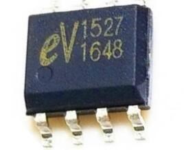 EV1527 Encoder IC: Datasheet pdf, equivalent and Circuit
19 November 202121743
 Stellaris® LM3S315 Microcontroller: Technical Overview
29 February 2024200
 OPA627AU Operational Amplifier: Pinout, Applications and Datasheet
19 October 20232628
 Unveiling the Texas Instruments MSP430F20x Microcontroller Series: A Comprehensive Analysis
29 February 2024212
 Understanding UARTs: The Basics and Benefits of Serial Communication
06 March 20233061
 Exploring the Cyber Physical System of Electric Vehicles
25 March 20242908
 Working Principles and Applications of Pressure Sensors
07 April 202535958
 AI Computing Power Gap: How Token Consumption is Reshaping Server Component Sourcing
23 June 2026174
 What is a SAW Sensor? Types, Working and Applications
29 March 202119889
 A Guide to Semiconductor IP Core
18 January 202210249
 Introduction to TFT Displays
29 August 20209568
 Understanding SiC MOSFET Power Modules and Ensuring its Short-Circuit Safety
15 March 20244245
Analog Devices Inc.
In Stock: 1000
Minimum: 1 Multiples: 1
Qty
Unit Price
Ext Price
1
$25.948165
$25.95
10
$24.479401
$244.79
100
$23.093774
$2,309.38
500
$21.786580
$10,893.29
1000
$20.553377
$20,553.38
Not the price you want? Send RFQ Now and we'll contact you ASAP.
Inquire for More Quantity
![ADV7513BSWZ]() ADV7513BSWZ
ADV7513BSWZAnalog Devices, Inc.
![AD9877ABSZ]() AD9877ABSZ
AD9877ABSZAnalog Devices, Inc.
![LTC2245CUH#TRPBF]() LTC2245CUH#TRPBF
LTC2245CUH#TRPBFLinear Technology/Analog Devices
![AD7791BRMZ-REEL]() AD7791BRMZ-REEL
AD7791BRMZ-REELAnalog Devices Inc.
![AD7799BRUZ-REEL]() AD7799BRUZ-REEL
AD7799BRUZ-REELAnalog Devices Inc.
![AD7190BRUZ-REEL]() AD7190BRUZ-REEL
AD7190BRUZ-REELAnalog Devices Inc.
![AD7705BRZ-REEL]() AD7705BRZ-REEL
AD7705BRZ-REELAnalog Devices Inc.
![AD7175-2BRUZ-RL7]() AD7175-2BRUZ-RL7
AD7175-2BRUZ-RL7Analog Devices Inc.
![AD7192BRUZ-REEL]() AD7192BRUZ-REEL
AD7192BRUZ-REELAnalog Devices Inc.
![AD9283BRSZ-RL100]() AD9283BRSZ-RL100
AD9283BRSZ-RL100Analog Devices Inc.


