Product
 Brand
Brand Articles
 Tools
Tools
How to Distinguish MOSFET? Is it N-Channel or P-Channel?
Mosfet Transistor: N-Channel and P-Channel
Metal Oxide Semiconductor Field Effect Transistor (MOSFET) is a basic component of modern electronic goods and is abbreviated as FET.
You may be familiar with MOSFETs as an electronic engineer, but have you truly mastered them? In this post, we'll go over the fundamentals of current and semiconductors, as well as the area and construction of MOSFETs and their circuit symbols.
First, let me ask you a question. Do you understand how the circuit's current and electrons flow?

Figure. 1
The electric field passes from the positive electrode to the negative electrode outside the battery in the circuit shown in Figure 1. Electrons move in the opposite direction from the electric field or current, from the negative electrode to the positive electrode.
The MOSFET is made of a semiconductor material like silicon, which possesses conductivity in the range of a conductor and an insulator. Two sorts of impurities are put into pristine crystals to make a semiconductor a good conductor. The resulting semiconductor is n-type if the impurities are pentavalent. The majority of charge carriers in n-type electrons. The resulting semiconductor is p-type if the impurities are trivalent. The majority of charge carriers are found in the p-type hole.

Figure. 2
If we join them, as shown in Figure 2, n-type electrons will fill the holes in the p-type at the junction, depleting the charge near the junction. The depletion region is the name given to this location. The depletion layer is minimized when the p-type is connected to the positive electrode of the battery and the n-type is connected to the negative electrode of the battery. which is known as forwarding bias. The depletion layer will rise if the battery's polarity is changed, which is known as reverse bias.
There are two types of MOSFETs: enhancement and depletion, which are further classified into N-channel and P-channel.
An N-channel MOSFET is the type of MOSFET we've been discussing. Let's start with N-channel enhancement-mode MOSFETs.

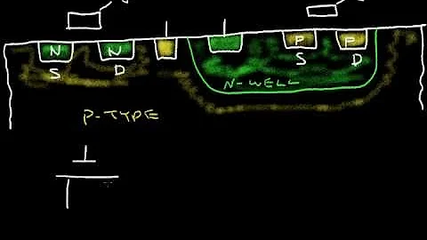
Figure. 3 The Structure of the MOSFET
The structure of the MOSFET is shown in Figure 3. An n-type semiconductor is shown in yellow, whereas a p-type semiconductor is shown in blue. The substrate or substrate terminal is the terminal attached to the blue. The source terminal is one of the two terminals connected to the yellow, while the drain terminal is the other. There is a thin layer of insulator or dielectric between these terminals, and another terminal termed the gate terminal, is attached above the insulator, As seen in Figure 4, the MOSFET's four terminals are as follows:

Figure. 4
The source and drain can be switched since the MOSFET is symmetrical. As a result of the internal connection between the source and substrate terminals, the MOSFET we observe has three terminals, all of which are at the same potential, preventing any current from flowing from the substrate to the source,
We want the current to flow from the drain to the source in a MOSFET. As a result, a battery must be connected between the drain and the source, Because it is between the drain and the source. this voltage is called Vds. In addition, as illustrated in Figure 5, we can see the link between the drain current and Vds.

Figure. 5
The positive electrode of the battery raises the voltage at the drain terminal, resulting in a larger depletion area between the drain and the substrate, preventing current from flowing from the drain to the source, The MOSFET is currently in the off state, commonly known as the Cutoff region.
A channel must now be built between the drain and the source in order for current to flow from the drain to the source, We put a tiny voltage source between the gate and the substrate to construct a channel, as shown in Figure 6:

Figure. 6
The gate is connected to the battery's positive terminal. Because it is between the gate and the source. this voltage is designated Vgs. A p-type semiconductor is used as the substrate. As a result, the charge carriers are holes, while there are a few free electrons in the mix. Inside the substrate, the battery creates an electric field. The electrons in the substrate move in the opposite direction of the electric field, to the grid, as a result of this field. These electrons cannot travel from the substrate to the grid due to the existence of an insulator. therefore they collect near the grid in the substrate.
Capacitors are known for storing charges on two metal plates. Similarly, by putting an insulator or dielectric between the plates, we can enhance capacitance. Similarly, in a MOSFET, the insulator or dielectric not only blocks electrons but also boosts their charge, attracting extra electrons.

Figure. 7
More electrons will be drawn to the gate as Vgs rises, and these electrons will begin to fill some holes. Similarly, they begin to move away from the gate because of the increased charge of the gate holes.
We can observe that there are no holes in the red box area illustrated in Figure 7 above, yet there are free electrons. The area surrounding the gate becomes a negative or n-type semiconductor as a result of these electrons, creating an internal dielectric. The channel is generated by connecting the source and drain, the channel can flow electrons from the source to the drain, and the channel thickness can be changed by altering the gate voltage. The width of the channel grows or decreases as the voltage increases or lowers. The voltage that forms the channel is referred to as the threshold voltage.

Figure. 8
As seen in Figure 8, the current can flow from the drain to the source through this channel after it has been created. The electron flow is from the source to the drain, whereas the current flows from the drain to the source Because the source supplies electrons to the channel and the drain collects electrons from the channel. they are referred to as source and drain. Drain current is named for the fact that it flows from the drain to the source,
When the MOSFET is in the ohmic or linear area, Ohm's law applies, which means that the current grows linearly as the voltage increases. However, when the voltage rises, the reverse bias expands the depletion zone between the drain and the substrate. Similarly, because the drain is at a positive potential, the channel begins to run out toward the drain end, and the negative charge from the channel closest to the drain is drawn into the drain, reducing the channel's width and so restricting charge flow. In addition, it lowers current flow. When we increase the voltage, the channel's entire contraction reaches a point known as the pinch-off effect. The channel is not totally constricted in real-world situations. Many electrons will linger in the channel due to the high volume of electrons flowing through it. A steady saturation current, rather than ceasing the current, is known as the saturation current, and the voltage at which the current occurs is known as the saturation voltage. If you raise the voltage, the reverse bias rises and the channel narrows even more, but the current does not rise because the channel is saturated, which is known as the saturation zone.
Because the amount of voltage on the gate controls the flow of current from the drain to the source. MOSFETs are also known as voltage control devices. Similarly, no current passes through the gate.

Figure. 9
The drain characteristic is on the left, while the transfer characteristic (constant Vds) is on the right, as shown in Figure 9.
Depletion mode MOSFETs are a different form of MOSFET. Except for the fact that the channel is produced during doping, it is comparable to the enhancement type in that it has a channel formed by the enhancement type gate voltage by default. The rest of the operating concepts are the same. The distinction is that the consumption is higher. The exhaust type, which requires a negative gate voltage to close, is typically open (generally closed), whereas the improved type is typically closed (normally open).

Figure. 10
Let's look at the circuit symbol for a MOSFET now that we've learned about its operating principle. As seen in Figure 10:
Each circuit symbol, as shown in Figure 10, has four terminals: the source. the gate, the drain, and the substrate, with the source and substrate being internally coupled. The N channel or electrons flow to the gate to form an N channel if the arrow points to the substrate; otherwise, the P channel or electrons flow away from the gate to generate a P channel,
 UTMEL
UTMEL
We are the professional distributor of electronic components, providing a large variety of products to save you a lot of time, effort, and cost with our efficient self-customized service. careful order preparation fast delivery service
1. What are the similarities and differences between JFET and MOSFET?
JFET is used for small signal processing, while MOSFET is mainly used in linear or switching power supplies
In terms of application classification, JFET is divided into N-channel and P-channel, and MOSFET is divided into 4 types of N-channel enhancement type, N-channel depletion type, P-channel enhancement type, and P-channel depletion type.
From the conductivity type, MOSFET is divided into vertical channel and lateral channel, and vertical channel is divided into VMOSFET, DMOSFET, UMOSFET
2. What is a switching MOSFET?
It is a type of field effect transistor (metal oxide field effect transistor). Compared with ordinary field effect transistors, it has the following characteristics: the resistance when it is turned on is small; the operating frequency is high (because the circuit is in the pulse working state, it requires The device can alternately switch between on and off quickly); the equivalent capacitance of the gate is small, etc. In addition, since the switching MOSFET works in the switching state, there is no requirement for linearity. Switching FETs are mainly used in switching power supplies.
3. How to connect the three terminals of the MOSFET field effect tube?
For the MOSFET type field effect tube, it has three electrodes, namely the gate G (control), the drain D and the source S (controlled). For the N-channel (the arrow points to the inner one of the gate) D , G is connected to high level (+), S is connected to low level (-), D and S are turned on (VGS is greater than the pinch-off voltage, about 1V, and the pinch-off voltage is different depending on the tube), the current direction is D-->S Generally, the voltage of G (relative to S) cannot be greater than 30V, otherwise it will break down! (Generally around 10V) At the same time, the withstand voltage at both ends of DS and the current that can be withstood are also taken into consideration (for example, 2N60B IDS=2A VDS=600V) and finally there is transconductance (gm)
 Modeling Wide Band-Gap Semiconductors for Enhanced PerformanceRakesh Kumar, Ph.D.31 January 20243533
The article delves into the challenges faced by silicon-based power electronic devices and highlights the potential of wide band-gap semiconductors. It also emphasizes the importance of modeling power semiconductor devices and provides insights into various models. For electrical energy conversion to be dependable and effective, power electronics and semiconductor device technologies are essential.
Read More Optimizing Energy Management with Non-Isolated DC-DC ConvertersRakesh Kumar, Ph.D.04 February 20243176
The article classifies DC-DC converters and discusses the benefits and limitations of them. It proposes a modified DC-DC converter topology that combines the Cuk and Positive Output Super Lift Luo topologies to achieve a higher voltage gain with fewer components.
Read More ‘6G Networks’ - Pioneering the Next Era of Connectivity And InnovationRakesh Kumar, Ph.D.18 March 20243524
The article provides a comprehensive overview of the evolving landscape of mobile networks, the requirements that will shape the future of mobile communication, and the innovative technologies driving the transition to 6G.
Read More Review of IoT-Based Smart Home Security Systems- Part 1Rakesh Kumar, Ph.D.28 March 20243929
The article discusses the evolution of IoT-based smart home security systems, integrating advanced technologies like Raspberry Pi, PIR sensors, and voice recognition for enhanced user experience and efficiency.
Read More Understanding Photodiodes: Working Principles and Applications - Part 2Rakesh Kumar, Ph.D.24 May 20244994
The article provides a comprehensive overview of photodiodes, focusing on their operational principles, key factors affecting their efficiency, advantages, and disadvantages, and highlights their diverse applications.
Read More
Subscribe to Utmel !
![7100123753]()
![7100041423]()
![7000068161]()
![7100082475, 100x915mm]()
![2608585492]() 2608585492
2608585492Robert Bosch
![06014A4170]() 06014A4170
06014A4170Robert Bosch
![F013SM20JB]() F013SM20JB
F013SM20JBDremel
![Loctite NC-OO Wick]() Loctite NC-OO Wick
Loctite NC-OO WickHenkel
![2608585499]() 2608585499
2608585499Robert Bosch
![Q-A-100]() Q-A-100
Q-A-100Menda