
 Product
 Brand
Brand Articles
 Tools
Tools
P82B96 Bipolar IC: Pinout, 3D Model and Datasheet


Surface Mount Tube 5V V Signal Buffers, Repeaters, Splitters 2V~15V V 7pF pF
The P82B96 is a bipolar IC that creates a non-latching, bidirectional, logic interface between the normal I2C-bus and a range of other bus configurations. Furthermore, Huge range of Semiconductors, Capacitors, Resistors and IcS in stock. Welcome RFQ.

Connecting Arduino with multiple I²C devices
P82B96 Pinout

Pinout
P82B96 CAD Model

symbol

footprint

3D Model
P82B96 Overview
The P82B96 is a bipolar IC that creates a non-latching, bidirectional, logic interface between the normal I2C-bus and a range of other bus configurations. It can interface I2C-bus logic signals to similar buses having different voltage and current levels. For example, it can interface to the 350 µA SMBus, to 3.3 V logic devices, and to 15 V levels and/or low-impedance lines to improve noise immunity on longer bus lengths. It achieves this interface without any restrictions on the normal I2C-bus protocols or clock speed. The IC adds minimal loading to the I2C-bus node, and loadings of the new bus or remote I2C-bus nodes are not transmitted or transformed to the local node. Restrictions on the number of I2C-bus devices in a system, or the physical separation between them, are virtually eliminated. Transmitting SDA and SCL signals via balanced transmission lines (twisted pairs) or with galvanic isolation (opto-coupling) is simple because separate directional Tx and Rx signals are provided. The Tx and Rx signals may be directly connected, without causing latching, to provide an alternative bidirectional signal line with I2C-bus properties.
This article provides you with a basic overview of the P82B96, including its pin descriptions, features and specifications, etc., to help you quickly understand what P82B96 is.
P82B96 Features
■ Bidirectional data transfer of I2C-bus signals
■ Isolates capacitance allowing 400 pF on Sx/Sy side and 4000 pF on Tx/Ty side
■ Tx/Ty outputs have 60 mA sink capability for driving low-impedance or high capacitive buses
■ 400 kHz operation over at least 20 meters of wire (see AN10148)
■ Supply voltage range of 2 V to 15 V with I2C-bus logic levels on Sx/Sy side independent of supply voltage
■ Splits I2C-bus signal into pairs of forward/reverse Tx/Rx, Ty/Ry signals for interface with opto-electrical isolators and similar devices that need unidirectional input and output signal paths.
■ Low power supply current
■ ESD protection exceeds 3500 V HBM per JESD22-A114, 250 V DIP package, 400 V SO package MM per JESD22-A115, and 1000 V CDM per JESD22-C101
■ Latch-up free (bipolar process with no latching structures)
■ Packages offered: DIP8, SO8 and TSSOP8
Specifications
- TypeParameter
- Factory Lead Time7 Weeks
- Mounting Type
The "Mounting Type" in electronic components refers to the method used to attach or connect a component to a circuit board or other substrate, such as through-hole, surface-mount, or panel mount.
Surface Mount - Package / Case
refers to the protective housing that encases an electronic component, providing mechanical support, electrical connections, and thermal management.
8-SOIC (0.154, 3.90mm Width) - Surface Mount
having leads that are designed to be soldered on the side of a circuit board that the body of the component is mounted on.
YES - Interface StandardsGENERAL PURPOSE
- Operating Temperature
The operating temperature is the range of ambient temperature within which a power supply, or any other electrical equipment, operate in. This ranges from a minimum operating temperature, to a peak or maximum operating temperature, outside which, the power supply may fail.
-40°C~85°C - Packaging
Semiconductor package is a carrier / shell used to contain and cover one or more semiconductor components or integrated circuits. The material of the shell can be metal, plastic, glass or ceramic.
Tube - Published2003
- JESD-609 Code
The "JESD-609 Code" in electronic components refers to a standardized marking code that indicates the lead-free solder composition and finish of electronic components for compliance with environmental regulations.
e4 - Part Status
Parts can have many statuses as they progress through the configuration, analysis, review, and approval stages.
Active - Moisture Sensitivity Level (MSL)
Moisture Sensitivity Level (MSL) is a standardized rating that indicates the susceptibility of electronic components, particularly semiconductors, to moisture-induced damage during storage and the soldering process, defining the allowable exposure time to ambient conditions before they require special handling or baking to prevent failures
1 (Unlimited) - Number of Terminations8
- TypeBuffer, ReDriver
- Terminal Finish
Terminal Finish refers to the surface treatment applied to the terminals or leads of electronic components to enhance their performance and longevity. It can improve solderability, corrosion resistance, and overall reliability of the connection in electronic assemblies. Common finishes include nickel, gold, and tin, each possessing distinct properties suitable for various applications. The choice of terminal finish can significantly impact the durability and effectiveness of electronic devices.
Nickel/Palladium/Gold (Ni/Pd/Au) - Applications
The parameter "Applications" in electronic components refers to the specific uses or functions for which a component is designed. It encompasses various fields such as consumer electronics, industrial automation, telecommunications, automotive, and medical devices. Understanding the applications helps in selecting the right components for a particular design based on performance, reliability, and compatibility requirements. This parameter also guides manufacturers in targeting their products to relevant markets and customer needs.
I2C - Voltage - Supply
Voltage - Supply refers to the range of voltage levels that an electronic component or circuit is designed to operate with. It indicates the minimum and maximum supply voltage that can be applied for the device to function properly. Providing supply voltages outside this range can lead to malfunction, damage, or reduced performance. This parameter is critical for ensuring compatibility between different components in a circuit.
2V~15V - Terminal Position
In electronic components, the term "Terminal Position" refers to the physical location of the connection points on the component where external electrical connections can be made. These connection points, known as terminals, are typically used to attach wires, leads, or other components to the main body of the electronic component. The terminal position is important for ensuring proper connectivity and functionality of the component within a circuit. It is often specified in technical datasheets or component specifications to help designers and engineers understand how to properly integrate the component into their circuit designs.
DUAL - Terminal Form
Occurring at or forming the end of a series, succession, or the like; closing; concluding.
GULL WING - Peak Reflow Temperature (Cel)
Peak Reflow Temperature (Cel) is a parameter that specifies the maximum temperature at which an electronic component can be exposed during the reflow soldering process. Reflow soldering is a common method used to attach electronic components to a circuit board. The Peak Reflow Temperature is crucial because it ensures that the component is not damaged or degraded during the soldering process. Exceeding the specified Peak Reflow Temperature can lead to issues such as component failure, reduced performance, or even permanent damage to the component. It is important for manufacturers and assemblers to adhere to the recommended Peak Reflow Temperature to ensure the reliability and functionality of the electronic components.
260 - Number of Functions2
- Supply Voltage
Supply voltage refers to the electrical potential difference provided to an electronic component or circuit. It is crucial for the proper operation of devices, as it powers their functions and determines performance characteristics. The supply voltage must be within specified limits to ensure reliability and prevent damage to components. Different electronic devices have specific supply voltage requirements, which can vary widely depending on their design and intended application.
5V - Time@Peak Reflow Temperature-Max (s)
Time@Peak Reflow Temperature-Max (s) refers to the maximum duration that an electronic component can be exposed to the peak reflow temperature during the soldering process, which is crucial for ensuring reliable solder joint formation without damaging the component.
30 - Base Part Number
The "Base Part Number" (BPN) in electronic components serves a similar purpose to the "Base Product Number." It refers to the primary identifier for a component that captures the essential characteristics shared by a group of similar components. The BPN provides a fundamental way to reference a family or series of components without specifying all the variations and specific details.
P82B96 - Output
In electronic components, the parameter "Output" typically refers to the signal or data that is produced by the component and sent to another part of the circuit or system. The output can be in the form of voltage, current, frequency, or any other measurable quantity depending on the specific component. The output of a component is often crucial in determining its functionality and how it interacts with other components in the circuit. Understanding the output characteristics of electronic components is essential for designing and troubleshooting electronic circuits effectively.
2-Wire Bus - Pin Count
a count of all of the component leads (or pins)
8 - JESD-30 Code
JESD-30 Code refers to a standardized descriptive designation system established by JEDEC for semiconductor-device packages. This system provides a systematic method for generating designators that convey essential information about the package's physical characteristics, such as size and shape, which aids in component identification and selection. By using JESD-30 codes, manufacturers and engineers can ensure consistency and clarity in the specification of semiconductor packages across various applications and industries.
R-PDSO-G8 - Qualification Status
An indicator of formal certification of qualifications.
Not Qualified - Number of Channels2
- Current - Supply
Current - Supply is a parameter in electronic components that refers to the maximum amount of electrical current that the component can provide to the circuit it is connected to. It is typically measured in units of amperes (A) and is crucial for determining the power handling capability of the component. Understanding the current supply rating is important for ensuring that the component can safely deliver the required current without overheating or failing. It is essential to consider this parameter when designing circuits to prevent damage to the component and ensure proper functionality of the overall system.
900μA - Input
In electronic components, "Input" refers to the signal or data that is provided to a device or system for processing or manipulation. It is the information or command that is received by the component to initiate a specific function or operation. The input can come from various sources such as sensors, other electronic devices, or user interactions. It is crucial for the proper functioning of the component as it determines how the device will respond or behave based on the input received. Understanding and managing the input parameters is essential in designing and using electronic components effectively.
2-Wire Bus - Driver Number of Bits2
- Receiver Number of Bits2
- Data Rate (Max)
Data Rate (Max) refers to the maximum rate at which data can be transferred or processed within an electronic component or device. It is typically measured in bits per second (bps) or megabits per second (Mbps). This parameter is important for determining the speed and efficiency of data transmission or processing in various electronic applications such as computer systems, networking devices, and memory modules. A higher data rate indicates that the component is capable of handling larger volumes of data at a faster pace, leading to improved performance and responsiveness in electronic systems. It is crucial to consider the Data Rate (Max) specification when selecting electronic components to ensure compatibility and optimal functionality for specific applications.
400kHz - Capacitance - Input
Capacitance - Input is a parameter that describes the input capacitance of an electronic component, such as a transistor or an integrated circuit. It represents the amount of charge that the input of the component can store when a voltage is applied to it. This capacitance affects the speed and performance of the component, as it can influence the time it takes for the input signal to be processed. A higher input capacitance can result in slower response times and may require additional circuitry to mitigate its effects. It is an important parameter to consider when designing and analyzing electronic circuits to ensure proper functionality and performance.
7pF - Length4.9mm
- Height Seated (Max)
Height Seated (Max) is a parameter in electronic components that refers to the maximum allowable height of the component when it is properly seated or installed on a circuit board or within an enclosure. This specification is crucial for ensuring proper fit and alignment within the overall system design. Exceeding the maximum seated height can lead to mechanical interference, electrical shorts, or other issues that may impact the performance and reliability of the electronic device. Manufacturers provide this information to help designers and engineers select components that will fit within the designated space and function correctly in the intended application.
1.75mm - Width3.9mm
- RoHS Status
RoHS means “Restriction of Certain Hazardous Substances” in the “Hazardous Substances Directive” in electrical and electronic equipment.
ROHS3 Compliant
P82B96 Functional Block Diagram

block diagram
P82B96 Equivalent
| Model number | Manufacturer | Description |
| P82B96PN,112 | NXP Semiconductors | P82B96 - Dual bidirectional bus buffer DIP 8-Pin |
| P82B96PE4 | Texas Instruments | DUAL LINE TRANSCEIVER, PDIP8, ROHS COMPLIANT, PLASTIC, DIP-8 |
| 935262297112 | NXP Semiconductors | IC SPECIALTY MICROPROCESSOR CIRCUIT, PDIP8, DIP-8, Microprocessor IC:Other |
| P82B96P | Texas Instruments | 2-bit bidirectional 2- to 15-V 400-kHz I2C/SMBus buffer/cable extender 8-PDIP -40 to 85 |
Parts with Similar Specs
- ImagePart NumberManufacturerPackage / CaseSupply VoltageInputMoisture Sensitivity Level (MSL)Factory Lead TimeLengthOutputPin CountView Compare
![P82B96TD,112]()
P82B96TD,112
8-SOIC (0.154, 3.90mm Width)
5 V
2-Wire Bus
1 (Unlimited)
7 Weeks
4.9 mm
2-Wire Bus
8
![PCA9600D,118]()
8-SOIC (0.154, 3.90mm Width)
3.3 V
2-Wire Bus
1 (Unlimited)
7 Weeks
4.9 mm
2-Wire Bus
8
![PCA9601D,118]()
8-SOIC (0.154, 3.90mm Width)
5 V
2-Wire Bus
1 (Unlimited)
7 Weeks
4.9 mm
2-Wire Bus
8
![PCA9600D,112]()
8-SOIC (0.154, 3.90mm Width)
5 V
2-Wire Bus
1 (Unlimited)
7 Weeks
4.9 mm
2-Wire Bus
8

P82B96 Application
■ Interface between I2C-buses operating at different logic levels (for example, 5 V and 3 V or 15 V)
■ Interface between I2C-bus and SMBus (350 µA) standard
■ Simple conversion of I2C-bu s SDA or SCL signals to multi-drop differential bus hardware, for example, via compatible PCA82C250
■ Interfaces with opto-couplers to provide opto-isolation between I2C-bus nodes up to 400 kHz
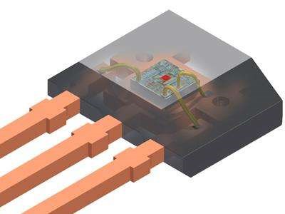
P82B96 Package

package
P82B96 Manufacturer
NXP Semiconductors is dedicated to providing secure connectivity solutions for embedded applications,the company has 45,000 employees in more than 35 countries.and has been operating,with its experience and expertise,for more than 60 years.As a leader in this field,NXP is driving innovation in the secure connected vehicle, end-to-end security & privacy and smart connected solutions markets,with the hope of making lives easier, better and safer Freescale Semiconductor parts are now a part of the NXP family.
Datasheet PDF
- Datasheets :
- Environmental Information :
- PCN Packaging :
Trend Analysis
What is the essential property of the P82B96?
The P82B96 is a bipolar IC that creates a non-latching, bidirectional, logic interface between the normal I²C-bus and a range of other bus configurations.
Can the P82B96 achieve high clock rates over long cables?
P82B96 can achieve high clock rates over long cables. While calculating with lumped wiring capacitance yields reasonable approximations to actual timing, even 25 meters of cable is better treated using transmission line theory.
For P82B96, how can the diode conduct in a particular application?
For the P82B96, in specific applications, there will always be transient overshoot and ringing on the wiring that can cause these diodes to conduct.
 2N2646 PN Unijunction Transistor: Datasheet, Pinout and Equivalent
21 October 202121107
 LPC824 Microcontroller: Datasheet, Pinout, NXP LPC824
23 August 20211995
![PMDXB950UPE 20 V dual P-channel Trench MOSFET[FAQ]](https://res.utmel.com/Images/Article/340113cd-663b-4721-83d8-46968f2d84a6.png) PMDXB950UPE 20 V dual P-channel Trench MOSFET[FAQ]
PMDXB950UPE 20 V dual P-channel Trench MOSFET[FAQ]19 April 2022499
 ntd24n06lt4g:an N-channel Power MOSFET
12 March 2022581
 BME280 Sensor: Datasheet, Pinout and Applications
08 July 202112904
 Advantech Corp 96MPXE-2.6-19M36: A Comprehensive Guide to the Discontinued Skylake Microprocessor Module
07 March 2024484
 1N4746A Zener Diode 18 V 1 W ±5% Through Hole DO-41:Datasheet, Mark information, and Equivalents
17 February 20222530
 ATTINY85-20SU Microcontroller: Circuit, Pinout, and Datasheet
21 February 20224876
 What is Field Programmable Gate Array(FPGA)?
27 April 20221132
 Latest Advances in Occupancy Sensor Detection Methods
14 July 20251188
 Vision Capabilities Are at the Heart of AI's Evolutionary Possession of Intelligence
06 July 20222207
 Will HBM replace DDR and become Computer Memory?
09 September 202123311
 Basic Introduction to Hall Effect Sensors
13 November 20258618
 Understanding the Basics of I2C Interface Controllers
11 June 20251194
 Microchip FPGA Solutions: Aerospace and Industrial Applications
09 June 2025619
 PMIC - Gate Drivers: A Purpose-Built Integrated Circuit
22 February 20233052
NXP USA Inc.
In Stock: 2
United States
China
Canada
Japan
Russia
Germany
United Kingdom
Singapore
Italy
Hong Kong(China)
Taiwan(China)
France
Korea
Mexico
Netherlands
Malaysia
Austria
Spain
Switzerland
Poland
Thailand
Vietnam
India
United Arab Emirates
Afghanistan
Åland Islands
Albania
Algeria
American Samoa
Andorra
Angola
Anguilla
Antigua & Barbuda
Argentina
Armenia
Aruba
Australia
Azerbaijan
Bahamas
Bahrain
Bangladesh
Barbados
Belarus
Belgium
Belize
Benin
Bermuda
Bhutan
Bolivia
Bonaire, Sint Eustatius and Saba
Bosnia & Herzegovina
Botswana
Brazil
British Indian Ocean Territory
British Virgin Islands
Brunei
Bulgaria
Burkina Faso
Burundi
Cabo Verde
Cambodia
Cameroon
Cayman Islands
Central African Republic
Chad
Chile
Christmas Island
Cocos (Keeling) Islands
Colombia
Comoros
Congo
Congo (DRC)
Cook Islands
Costa Rica
Côte d’Ivoire
Croatia
Cuba
Curaçao
Cyprus
Czechia
Denmark
Djibouti
Dominica
Dominican Republic
Ecuador
Egypt
El Salvador
Equatorial Guinea
Eritrea
Estonia
Eswatini
Ethiopia
Falkland Islands
Faroe Islands
Fiji
Finland
French Guiana
French Polynesia
Gabon
Gambia
Georgia
Ghana
Gibraltar
Greece
Greenland
Grenada
Guadeloupe
Guam
Guatemala
Guernsey
Guinea
Guinea-Bissau
Guyana
Haiti
Honduras
Hungary
Iceland
Indonesia
Iran
Iraq
Ireland
Isle of Man
Israel
Jamaica
Jersey
Jordan
Kazakhstan
Kenya
Kiribati
Kosovo
Kuwait
Kyrgyzstan
Laos
Latvia
Lebanon
Lesotho
Liberia
Libya
Liechtenstein
Lithuania
Luxembourg
Macao(China)
Madagascar
Malawi
Maldives
Mali
Malta
Marshall Islands
Martinique
Mauritania
Mauritius
Mayotte
Micronesia
Moldova
Monaco
Mongolia
Montenegro
Montserrat
Morocco
Mozambique
Myanmar
Namibia
Nauru
Nepal
New Caledonia
New Zealand
Nicaragua
Niger
Nigeria
Niue
Norfolk Island
North Korea
North Macedonia
Northern Mariana Islands
Norway
Oman
Pakistan
Palau
Palestinian Authority
Panama
Papua New Guinea
Paraguay
Peru
Philippines
Pitcairn Islands
Portugal
Puerto Rico
Qatar
Réunion
Romania
Rwanda
Samoa
San Marino
São Tomé & Príncipe
Saudi Arabia
Senegal
Serbia
Seychelles
Sierra Leone
Sint Maarten
Slovakia
Slovenia
Solomon Islands
Somalia
South Africa
South Sudan
Sri Lanka
St Helena, Ascension, Tristan da Cunha
St. Barthélemy
St. Kitts & Nevis
St. Lucia
St. Martin
St. Pierre & Miquelon
St. Vincent & Grenadines
Sudan
Suriname
Svalbard & Jan Mayen
Sweden
Syria
Tajikistan
Tanzania
Timor-Leste
Togo
Tokelau
Tonga
Trinidad & Tobago
Tunisia
Turkey
Turkmenistan
Turks & Caicos Islands
Tuvalu
U.S. Outlying Islands
U.S. Virgin Islands
Uganda
Ukraine
Uruguay
Uzbekistan
Vanuatu
Vatican City
Venezuela
Wallis & Futuna
Yemen
Zambia
Zimbabwe
![PCA9617ADPJ]() PCA9617ADPJ
PCA9617ADPJNXP USA Inc.
![PCA9515ADP,118]() PCA9515ADP,118
PCA9515ADP,118NXP USA Inc.
![PCA9615DPJ]() PCA9615DPJ
PCA9615DPJNXP USA Inc.
![PCA9517ADP,118]() PCA9517ADP,118
PCA9517ADP,118NXP USA Inc.
![P82B96TD,118]() P82B96TD,118
P82B96TD,118NXP USA Inc.
![PCA9600DP,118]() PCA9600DP,118
PCA9600DP,118NXP USA Inc.
![P82B96DP,118]() P82B96DP,118
P82B96DP,118NXP USA Inc.
![PCA9517DP,118]() PCA9517DP,118
PCA9517DP,118NXP USA Inc.
![PCA9511ADP,118]() PCA9511ADP,118
PCA9511ADP,118NXP USA Inc.
![PCA9512ADP,118]() PCA9512ADP,118
PCA9512ADP,118NXP USA Inc.

