

 Product
 Brand
Brand Articles
 Tools
Tools
Photonic Chip Computing: Architecture, Physical Limits, and the Path from Lab to Market
Photonic chip computing is an emerging hardware paradigm that uses photons rather than electrons to execute high-dimensional linear algebra and transport data across integrated circuits. By utilizing light propagation through silicon waveguides, photonic systems eliminate resistive heat losses in interconnects and perform analog matrix calculations at the speed of light. However, photonics does not replace electronic complementary metal-oxide-semiconductor (CMOS) microprocessors. Instead, commercial adoption relies on hybrid electro-photonic co-packaging, where silicon photonics handles massive data movement[4] and parallel matrix math while digital electronics manages control flow, non-linear operations, and static memory.
The standard system execution pipeline partitions workloads between electronic host processors and optical acceleration dies:
Host Electronic CMOS Die: Executes instruction dispatch, control logic, and weight/activation streaming from SRAM or High-Bandwidth Memory.
Mixed-Signal Interface & Drivers: Converts digital weights and activations into high-speed analog drive signals via DACs and laser modulator drivers.
Photonic Integrated Circuit (PIC) Die: Routes external continuous-wave laser light (such as 1310 nm or 1550 nm DFB sources) through coherent MZI meshes or incoherent WDM microring resonator banks to execute matrix transformations, followed by integrated germanium photodetectors.
Amplification & Digitization: Transimpedance amplifiers (TIAs) and ADCs convert resulting analog photocurrents back into digitized partial sums.
Non-Linear Activation Processing: The electronic CMOS die applies non-linear activation functions (such as ReLU, GELU, or Softmax) before memory storage or subsequent layer dispatch.
The Architectural Taxonomy: Optical Interconnects versus Photonic Compute
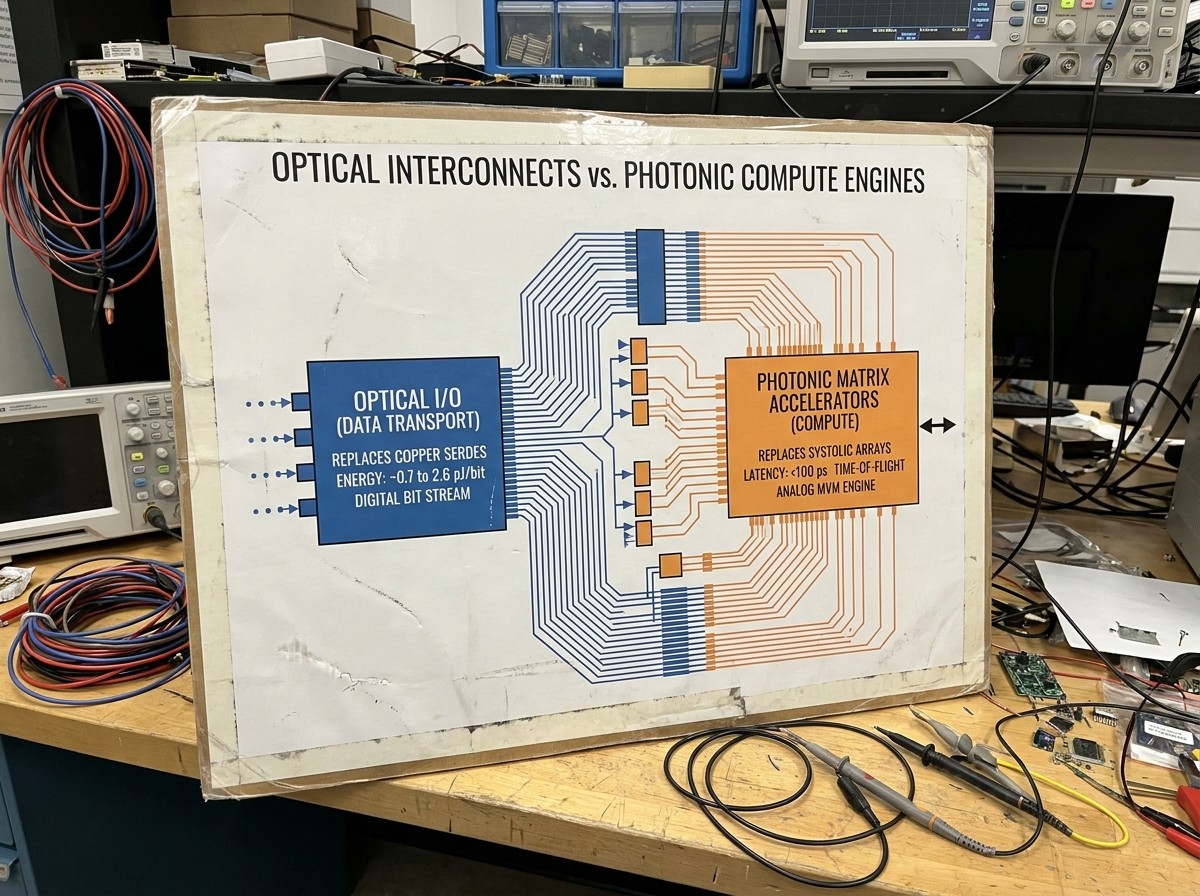
The integrated photonics industry is bifurcated into two architectural domains: optical input/output (Optical I/O) for data transport and optical matrix accelerators for mathematical processing. Confusing these two paradigms leads to unrealistic assumptions about what optical hardware delivers in commercial data centers.
Optical I/O and Co-Packaged Optics for Data Transport
Optical I/O replaces high-loss electrical copper traces and power-hungry serializer/deserializer (SerDes) circuits with fiber-optic links directly at the chip package boundary. In modern distributed machine learning clusters, electrical interconnects hit an energy wall: driving high-frequency electrical signals over printed circuit board (PCB) traces consumes 15 to 30+ picojoules per bit () over long channels with retimers.
In-package optical I/O lowers this transport penalty. For example, Ayar Labs' TeraPHY optical I/O chiplet achieves up to 8 terabits per second () of bi-directional bandwidth with sub-10 nanosecond () latency and an energy efficiency under. When utilizing dynamic microring macros atPAM4, efficiency reaches approximately, sustaining transmission reaches from millimeters up to 2 kilometers without Forward Error Correction () overhead.
By co-packaging optical engines with host graphics processing units (GPUs) or central processing units (CPUs), architects break the "memory wall" and interconnect bottlenecks while leaving the underlying digital compute architecture intact, following low-energy optical communications principles[6].
Photonic Tensor Accelerators for Mathematical Calculation
Photonic tensor accelerators use the physics of light interference and absorption to execute mathematical calculations directly in the analog optical domain. Rather than switching transistors on and off to evaluate binary logic, these engines encode numerical vectors into the amplitude, phase, or wavelength of light beams.
As light traverses a network of optical waveguides, operations such as General Matrix-to-Matrix Multiplications () occur continuously during photon time-of-flight. The propagation latency across an optical core is typically under().
This calculation mode is inherently analog. The computational output corresponds to the optical power or phase detected at an integrated photodiode, transforming complex linear algebra into a physical transmission property of the medium.
| Feature Dimension | Optical I/O / Co-Packaged Optics | Photonic Tensor Accelerators |
|---|---|---|
| Primary Objective | Move digital data with low loss | Execute analog linear algebra |
| Computational Domain | Digital (Bits retained end-to-end) | Analog (Phase/Intensity encoded) |
| Core Building Blocks | Transceivers, ELSFP lasers, SerDes | MZI meshes, MRR arrays, PDs |
| Direct Replacement For | Copper traces, PCIe/CXL cables | Electronic Tensor / Systolic Cores |
The Hybrid Heterogeneous Reality of Electro-Photonic Co-Design
"All-optical" general-purpose computers do not exist in commercial roadmaps because photons cannot be held statically at rest without active recirculation cavities or complex non-linear material traps. There is no physical equivalent of dense, non-volatile optical Random Access Memory () or static electronic registers ().
The hybrid computing split allocates tasks according to physical strengths:
Electronic CMOS Subsystem: High-density memory (HBM3e / SRAM), control logic, branch prediction, non-linear activations (GELU, ReLU), and high-precision deterministic calculations.
Photonic Integrated Circuit (PIC): Terabit-scale die-to-die I/O, passive low-latency GEMM / MVM acceleration, wavelength-multiplexed dot products, and streaming optical interposers.
Photons are ideal for streaming data and parallel linear transformations, while electrons remain essential for non-linear operations, logical branching, and static state retention. Consequently, modern photonic processors are fundamentally heterogeneous systems: silicon photonic integrated circuits () handle linear operations and interconnect fabrics, while bonded electronic integrated circuits () supply memory, system orchestration, and intermediate state control.
The Physics of Light-Based Calculation: How Photons Execute Linear Algebra
To understand how photonic chips compute without arithmetic logic units (), one must analyze how physical wave manipulation maps to linear matrix algebra. Modern photonic computing relies on two primary physical mechanisms: coherent spatial interference and incoherent wavelength multiplexing.
Google Tech Talk: optical matrix multiplication units in TPU ...
Coherent Mach-Zehnder Interferometer Meshes and Unitary Matrix Decomposition
A Mach-Zehnder Interferometer () consists of an input optical splitter, two internal propagation arms with phase shifters (and), and an output directional coupler. When coherent light enters the MZI, it splits across both arms. By adjusting the phase shifters via thermal or electro-optic modulation, the system controls how the two light paths interfere at the output, either constructively, destructively, or at intermediate amplitudes.
An individual MZI acts as an analogunitary matrix operator. To calculate arbitrarymatrix transformations, foundries construct planar meshes of hundreds of interconnected MZIs. As demonstrated in a programmable nanophotonic processor for arbitrary optical transformations[1], any real or complex matrixcan be factored using Singular Value Decomposition ():
Where:
and
are
unitary matrices.
is a diagonal matrix containing the singular values (scaling factors).
In a Clements rectangular mesh topology, the unitary matricesandare directly synthesized through programmed phase shifts () across directional couplers. The diagonal matrixis implemented using optical attenuators or variable gain amplifiers.
When an optical vector(encoded as coherent light amplitudes acrossinput waveguides) enters the mesh, it undergoes passive physical interference through, diagonal scaling via, and a final rotation through. The resulting optical field exiting the final waveguide array represents the calculated matrix-vector product.
Wavelength-Division Multiplexed Microring Resonators for Dot-Product Multiplication
The second core mechanism relies on microring resonators () operating across multiple optical wavelengths. Wavelength-Division Multiplexing () allows several independent data streams to travel down a single silicon waveguide concurrently without mutual interference.
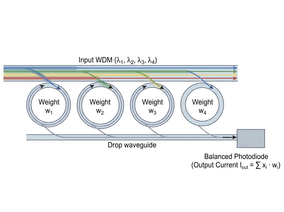
In an MRR dot-product engine:
Vector Encoding: Elements of an input vector
are modulated onto discrete optical carrier wavelengths
.
Weight Modulation: The multiplexed beam travels past a bank of microring resonators. Each microring is tuned to couple with a specific wavelength
. By shifting the ring's resonance relative to the carrier wavelength, the device attenuates the optical transmission, multiplying
by a weight value
.
Passive Summation: The transmitted optical signals drop into an output waveguide and land on a wideband photodetector. The photodiode converts the combined optical power into an electrical current through natural photocurrent superposition:
MRR-based systems occupy a much smaller physical footprint than MZI meshes (ring diameters compared to hundreds of micrometers for MZIs). However, they are sensitive to thermal fluctuations and optical crosstalk between tightly spaced spectral channels.
Non-Linearity and Activation Functions in the Optical Domain
While linear matrix algebra () maps directly onto passive optical hardware, non-linear activation functions (such as,, or) present a fundamental physical challenge. Photons do not interact with other photons under standard operating conditions in silicon.
To execute non-linear activations in practical hardware, architectures rely on two methods:
Optical-Electrical-Optical () Execution (Current Production): Photodetectors convert linear optical dot products into electrical currents. Electronic CMOS circuits evaluate the non-linear function using digital lookup tables or analog threshold circuits before re-modulating the result onto light for the subsequent layer. While functionally robust, repeated
conversions introduce mixed-signal latency and power overhead.
All-Optical Non-Linear Materials (Research Frontier): Researchers explore a reconfigurable light-responsive non-linear architecture[7] using materials with high non-linear optical susceptibilities (such as graphene overlays, phase-change materials like
, or saturable absorbers). When light intensity passes a given threshold, the material changes its absorption or refractive index, altering transmission non-linearly without converting the signal back to electricity. These materials remain difficult to standardize in commercial 300 mm CMOS foundry lines due to optical power constraints and endurance limitations.
Engineering Bottlenecks and Physical Scaling Realities
Understanding why photonic chips have not completely displaced silicon microprocessors requires analyzing the physical scaling constraints of light, mixed-signal conversion limits, and thermal physics.
The Optical Diffraction Limit versus Nanometer CMOS Scaling
Electronic transistors scale to single-digit nanometer dimensions because an electron's de Broglie wavelength is sub-nanometer. In contrast, integrated silicon photonics operates in standard optical telecommunication bands: the O-band () and C-band ().
The minimum physical dimension of an optical waveguide is bounded by the fundamental diffraction limit:
Where:
is the operational wavelength in free space.
is the refractive index of the core material (
at
).
In single-mode silicon waveguides, the cross-sectional core dimensions are roughly. A fully functional MZI phase-shifting arm or directional coupler spans tens to hundreds of micrometers () in length to achieve sufficient optical phase delay without severe insertion loss.
Because an individual optical processing node is orders of magnitude larger than an electronic CMOS transistor, building a general-purpose microprocessor containing billions of optical logic gates on a single die is physically impossible. Photonic computing is therefore targeted at high-dimensional matrix acceleration where single optical operations replace hundreds of parallel digital arithmetic operations.
The Mixed-Signal Conversion Penalty: DAC and ADC Power Overhead
The primary consumer of energy and latency in analog photonic accelerators is not the optical propagation path—which is passive—but the electro-optical domain boundary.
Data stored in system memory is digital. To process this data optically, high-speed Digital-to-Analog Converters () must modulate electrical voltages onto optical carriers. After the light traverses the waveguide mesh, high-speed Analog-to-Digital Converters () must digitize the resulting photodiode currents back into binary words for memory storage, where designers must overcome the bottleneck of electronic jitter[3].
Peripheral DACs, ADCs, transimpedance amplifiers (), and modulator driver circuits account for approximately 70% to >85% of total system power dissipation in analog photonic AI accelerators.
Architectural Decision Rule: An analog photonic compute engine cannot achieve net system-level energy efficiency over digital CMOS on small, iterative operations. Net energy efficiency only emerges when matrix dimensions are large enough (e.g.,) to amortize the mixed-signal conversion overhead across thousands of continuous optical multiply-accumulate calculations.
Analog Signal-to-Noise Ratio and Numerical Precision Bounds
Digital electronic ALUs provide exact, deterministic numerical precision (such as IEEE 754 standard FP32 or FP64). Analog photonic computation is fundamentally non-deterministic, constrained by the physical Signal-to-Noise Ratio () of the optical channel and component imprecisions in optical neural networks[2].
Key physical noise mechanisms include:
Laser Relative Intensity Noise (RIN)
Waveguide phase crosstalk and manufacturing tolerances
Photodetector thermal and shot noise
Thermal phase drift across waveguide arms
These noise mechanisms limit the system's Effective Number of Bits (). While digital floating-point ALUs easily sustain 16-bit to 64-bit precision, analog photonic matrix accelerators are practically bounded to low-to-medium precision: 4-bit to 8-bit ENOB.
Consequently, photonic matrix accelerators cannot support high-precision scientific simulations or raw FP64 numerical computing. However, they are well-matched to deep learning inference workloads (such as INT8 and FP8 quantization regimes), where deep neural networks naturally tolerate small amounts of bounded analog noise.
Thermal Drift, Phase Jitter, and Dynamic Tuning Overhead
Silicon exhibits a high thermo-optic coefficient:
Because the refractive index () changes significantly with temperature, an ambient thermal drift of as little asalters the optical phase inside an MZI waveguide or shifts the narrow resonance peak of a microring resonator completely off its target wavelength grid.
To maintain computational accuracy, photonic integrated circuits must implement dedicated active micro-heaters, thermo-electric coolers (), or dynamic bias-tracking feedback loops across thousands of interferometers. The electrical energy consumed by these thermal stabilization circuits must be accounted for in the net system power budget.
Technical Comparison: Electronic CMOS versus Photonic Architectures
Evaluating photonic computing against conventional semiconductor hardware requires an objective breakdown of performance characteristics, energy dissipation, and physical trade-offs.
Comparative Technical Evaluation: Electronic CMOS vs. Hybrid Photonic Computing Architectures
| Evaluation Dimension | Conventional Electronic CMOS (GPU / TPU) | Co-Packaged Optical I/O + Electronic Compute | Coherent MZI Photonic Matrix Accelerator | Incoherent WDM Microring Photonic Accelerator |
|---|---|---|---|---|
| Primary Acceleration Target | Digital logic, general tensor math, control flow | Die-to-die and chip-to-memory interconnect bandwidth | Analog linear algebra (/ matrix-vector multiplication) | Wavelength-parallel analog dot products |
| Interconnect Energy | 15–30+(long copper SerDes channels) | ~0.7–2.6(in-package optical link) | Dependent on host interconnect | Dependent on host interconnect |
| Compute Latency per Matrix Operation | Clock-cycle dependent (nanoseconds to microseconds) | Standard CMOS execution (interconnect latency reduced) | Sub-nanosecond time-of-flight propagation () | Sub-nanosecond time-of-flight propagation () |
| Numerical Precision Support | High & Deterministic: INT4 to FP64 | Native to host CMOS (INT4 to FP64) | Low-to-Medium: ~4 to 8-bit ENOB (analog SNR bounded) | Low-to-Medium: ~4 to 7-bit ENOB (crosstalk bounded) |
| Static Memory Capability | Massive native SRAM & HBM3e integration | Standard electronic HBM/SRAM access | None (requires continuous electronic streaming) | None (requires continuous electronic streaming) |
| Physical Component Footprint | Nanometer scale (gate dimensions) | Mixed: nanometer CMOS + micrometer photonics | Micrometer scale (per MZI cell) | Micrometer scale (per ring) |
| Dominant Power Consumer | Charging parasitic wire capacitance & leakage | Electro-optical transceivers & laser bias | Mixed-signal DAC/ADC conversion (70–85%+ of power) | Mixed-signal DAC/ADC & thermal stabilization heaters |
| Primary Industry Sweet Spot | General AI training, branching logic, high precision | AI cluster scale-up fabrics, disaggregated memory | Latency-critical INT8/FP8 inference, streaming signal processing | Ultra-dense edge inference, WDM spectral filtering |
Practical Architecture Decision Framework
Hardware architects must evaluate their workload constraints before adopting photonic computing options:
Scenario A: Workloads Requiring Complex Control Flow or High Deterministic Precision (FP32/FP64)
Implementation: Traditional Electronic CMOS (GPUs/TPUs).
Rationale: General-purpose instruction logic, scalar branching, and high-precision scientific simulations are inefficient on analog optical engines due to SNR noise bounds and the lack of native optical logic gates.
Scenario B: Large-Scale AI Clusters Facing Interconnect and Memory Bandwidth Scaling Limits
Implementation: Co-Packaged Optics (
) and In-Package Optical I/O.
Rationale: Offloads inter-die data movement to optical fibers, cutting transport energy from
to
while retaining standard digital CMOS computation and software stacks.
Scenario C: High-Throughput, Ultra-Low-Latency Deep Learning Inference (INT8/FP8)
Implementation: Heterogeneous Coherent MZI or WDM Microring Accelerators.
Rationale: Matrix dimensions can be amortized across the optical mesh to take advantage of sub-nanosecond physical propagation speeds, provided the workload tolerates low-to-medium analog bit resolution.
Foundry Commercialization, Heterogeneous Integration, and Advanced Packaging
The transition of photonic computing from academic physics laboratories to high-volume commercial markets depends entirely on compatibility with existing semiconductor fabrication foundries.
300 mm Silicon-on-Insulator Manufacturing and Foundry PDKs
Rather than building dedicated manufacturing facilities, the silicon photonics industry utilizes standardandCMOS semiconductor foundries running Silicon-on-Insulator () wafers. This allows optical chips to leverage decades of lithographic precision, yield management, and cleanroom automation.
Foundries provide standardized Process Design Kits () containing pre-characterized optical building blocks:
Single-mode silicon and silicon nitride (
) waveguides with propagation losses below
.
Germanium (
) photodetectors with absorption bandwidths exceeding
.
High-speed electro-optic modulators based on carrier injection or depletion.
For example, GlobalFoundries' monolithicGF Fotonix platform (45SPCLO, based on a 45 nm SOI process) integrates RF-CMOS and passive/active photonic components onto a single die. The platform incorporatesPAM4 Mach-Zehnder and microring modulators, Ge photodetectors, and low-loss SiN waveguides, achieving integrated monolithic electronic-photonic transceiver power consumption of approximatelyat.
The Direct Bandgap Challenge and Heterogeneous III-V Laser Integration
Silicon is an indirect bandgap semiconductor; electrons transitioning between its conduction and valence bands release energy primarily as lattice vibrations (phonons) rather than photons. Consequently, silicon cannot act as an efficient laser light source.
To supply light to photonic integrated circuits, the industry uses three primary integration strategies:
Heterogeneous Direct Bonding: Epitaxial dies or wafers of III-V direct bandgap compound semiconductors (such as Indium Phosphide /
or Gallium Arsenide /
) are bonded to the silicon wafer via molecular or plasma bonding. Light generated in the III-V layer couples evanescently into underlying silicon waveguides.
Micro-Transfer Printing: Pre-fabricated, fully tested micro-scale laser diodes are mechanically picked and printed directly into pre-etched cavities on the silicon wafer surface, improving material utilization and overall yield.
External Laser Small Form-Factor Pluggables (): The laser light source is removed from the compute package entirely and housed in a separate, field-replaceable rack-mounted module. Light enters the photonic chip via optical fiber arrays. This approach eliminates the thermal load of the laser from the compute die and improves field serviceability.
Advanced 3D Packaging and Direct Hybrid Bonding
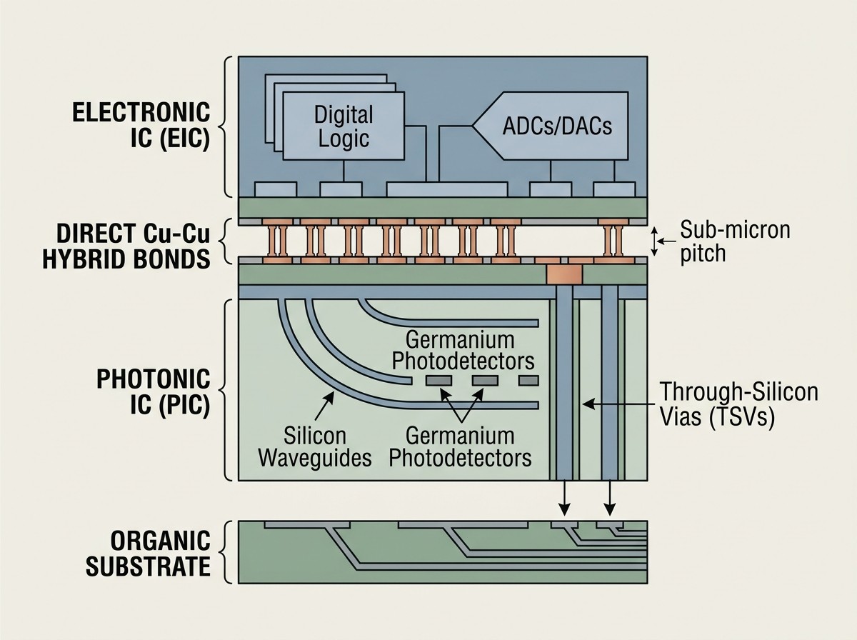
Early silicon photonic systems connected separate electronic control dies and photonic dies using lateral micro-bumps or wire bonds. However, the parasitic capacitance and inductance of these interconnects degraded transmission speeds and inflated mixed-signal DAC/ADC power consumption.
Modern implementations use true 3D heterogeneous stacking, placing the Electronic Integrated Circuit () directly atop the Photonic Integrated Circuit () using sub-micron pitch copper-to-copper direct hybrid bonding. In particular, TSMC's COUPE (Compact Universal Photonic Engine)[8] utilizes SoIC-X (System-on-Integrated-Chips) true 3D hybrid bonding to stack an Electronic IC directly atop a Photonic IC with over 99% stacking yield and ultra-low interface impedance.
By eliminating the parasitic capacitance of standard wire bonding, this 3D packaging method lowers interface power dissipation and reduces physical transceiver footprints. TSMC's packaging roadmap integrates these engines into small-form-factor pluggables (OSFP) and Co-Packaged Optics on CoWoS (Chip-on-Wafer-on-Substrate) systems scaling up toand.
Industry Standardization Frameworks Across OIF and UCIe
Photonic chip computing has moved past custom proprietary interfaces toward unified standards established by international consortiums:
Optical Internetworking Forum (): The OIF drives the Compute Optics Interface (COI) Framework[5], which defines interoperability agreements for co-packaged optical transceivers, electrical channel boundaries (such as
and next-generation
specifications), and standardized form factors for external laser light sources (
).
Universal Chiplet Interconnect Express (): The UCIe consortium incorporates optical extension workstreams within its chiplet standards. This enables host processors to interface with external optical I/O chiplets using uniform die-to-die protocols, creating a multi-vendor supply chain for co-packaged silicon photonics.
Summary and Next-Step Engineering Resources
Photonic chip computing is entering commercial infrastructure not as an all-optical CPU replacement, but as an essential co-packaged accelerator and interconnect layer.
Key architectural takeaways include:
Interconnect Scaling: Optical I/O cuts die-to-die transport power to <2.6 pJ/bit at terabit-scale bandwidth.
Matrix Math Acceleration: MZI and MRR meshes compute analog GEMM at sub-100 ps latency for low-precision INT8/FP8 workloads.
Foundry Standardization: 300 mm SOI wafer processing and 3D hybrid bonding integrate photonics directly into standard fab flows.
Engineering Next Steps
For hardware designers, system architects, and engineers evaluating integrated photonic technologies:
Explore Open-Source Silicon Photonic Process Design Kits: Experiment with layout and design frameworks such as SiEPIC (Silicon Photonics Electronic-Photonic Integrated Circuits) or open-source PDKs for KLayout to understand waveguide routing rules, bend radii constraints, and directional coupler geometries.
Model Mixed-Signal System Overheads: Utilize open-source numerical and electromagnetic simulation tools (such as Meep for FDTD analysis or Lumerical suites) to model insertion loss, phase jitter, and DAC/ADC power trade-offs before committing to optical tensor accelerator topologies.
Review Industry Standard Implementation Agreements: Study the Optical Internetworking Forum's Compute Optics Interface (
) white papers and UCIe chiplet interface roadmaps to ensure system designs conform to evolving Co-Packaged Optics specifications.
Technical Frequently Asked Questions
Can photonic chips completely replace electronic transistors in microprocessors?
No. Photonic chips cannot replace general-purpose microprocessors due to the optical diffraction limit (which constrains component sizes to micrometers), the lack of native optical static memory (orequivalents), and the difficulty of executing non-linear control logic optically. Photonic hardware operates as an accelerator alongside digital electronic CMOS.
Why are DAC and ADC converters a primary bottleneck in optical computing?
Optical matrix multiplication takes place in the analog domain, whereas system memory and instruction sets operate in the digital domain. Converting digital signals to analog voltages for optical modulators and converting analog photocurrents back to digital bits via ADCs consumes 70% to >85% of total accelerator subsystem energy. These mixed-signal conversion costs must be amortized over large matrix calculations to achieve net system efficiency.
How do ambient temperature variations affect photonic computing accuracy?
Silicon has a high thermo-optic coefficient (). Ambient temperature shifts change the refractive index of waveguides, inducing phase errors in Mach-Zehnder Interferometers and shifting the resonance peaks of Microring Resonators off their carrier wavelengths. Photonic chips use active on-chip micro-heaters, dynamic bias tracking, and thermal feedback loops to maintain optical stability.
What numerical precision can photonic tensor accelerators achieve?
Due to physical noise sources such as laser relative intensity noise (), photodiode shot noise, thermal jitter, and optical waveguide crosstalk, integrated photonic accelerators operate at an Effective Number of Bits () between 4-bit and 8-bit precision. This makes them well suited for quantization-resilient deep learning inference (and), while high-precision scientific computing (/) remains on digital CMOS.
What is the difference between Co-Packaged Optics and Optical Compute?
Co-Packaged Optics () focuses on data transport, replacing electrical copper traces with optical links inside the chip package to reduce transmission energy and increase bandwidth without modifying the host compute architecture. Optical Compute focuses on mathematical calculation, using optical wave interference or spectral transmission to execute linear matrix operations directly within the optical domain.
References
Programmable nanophotonic processor for arbitrary optical transformations — Massachusetts Institute of Technology / Nature Photonics
Design of optical neural networks with component imprecisions — Optica Publishing Group (Optics Express)
Photonic ADC: overcoming the bottleneck of electronic jitter — MIT Lincoln Laboratory / Optica Publishing Group (Optics Express)
Silicon Photonics for Scalable and Sustainable AI Hardware — IEEE Journal of Selected Topics in Quantum Electronics
Compute Optics Interface (COI): Energy Efficient Photonic Interconnects for AI Compute Scale-up White Paper — Optical Internetworking Forum (OIF)
Silicon Photonics for Low-Energy Optical Communications — Sandia National Laboratories
Reconfigurable Light-Responsive Non-Linear Architecture for Photonic Accelerators — National University of Singapore College of Design and Engineering
Silicon Photonics Platform for Next Generation Data Communication Technologies (COUPE) — Taiwan Semiconductor Manufacturing Company (TSMC)
 UTMEL
UTMEL
We are the professional distributor of electronic components, providing a large variety of products to save you a lot of time, effort, and cost with our efficient self-customized service. careful order preparation fast delivery service
 Discovering New and Advanced Methodology for Determining the Dynamic Characterization of Wide Bandgap DevicesSaumitra Jagdale15 March 20242900
For a long era, silicon has stood out as the primary material for fabricating electronic devices due to its affordability, moderate efficiency, and performance capabilities. Despite its widespread use, silicon faces several limitations that render it unsuitable for applications involving high power and elevated temperatures. As technological advancements continue and the industry demands enhanced efficiency from devices, these limitations become increasingly vivid. In the quest for electronic devices that are more potent, efficient, and compact, wide bandgap materials are emerging as a dominant player. Their superiority over silicon in crucial aspects such as efficiency, higher junction temperatures, power density, thinner drift regions, and faster switching speeds positions them as the preferred materials for the future of power electronics.
Read More Applications of FPGAs in Artificial Intelligence: A Comprehensive GuideUTMEL29 August 20255655
This comprehensive guide explores FPGAs as powerful AI accelerators that offer distinct advantages over traditional GPUs and CPUs. FPGAs provide reconfigurable hardware that can be customized for specific AI workloads, delivering superior energy efficiency, ultra-low latency, and deterministic performance—particularly valuable for edge AI applications. While GPUs excel at parallel processing for training, FPGAs shine in inference tasks through their adaptability and power optimization. The document covers practical implementation challenges, including development complexity and resource constraints, while highlighting solutions like High-Level Synthesis tools and vendor-specific AI development suites from Intel and AMD/Xilinx. Real-world applications span telecommunications, healthcare, autonomous vehicles, and financial services, demonstrating FPGAs' versatility in mission-critical systems requiring real-time processing and minimal power consumption.
Read More The 2026 Engineer’s Guide: Choosing the Right MCU for Your Next IoT & New Energy ProjectUTMEL30 April 20261969
A comprehensive comparison of 2026's leading MCUs from ST, NXP, and Microchip across power efficiency, processing performance, connectivity, and ecosystems to help engineers select the optimal chip for next-gen IoT and new energy projects.
Read More AI Server Components: Engineering Next-Gen Data Center Hardware for 100kW RacksUTMEL15 May 20261049
The transition from traditional enterprise IT to AI-driven workloads has rendered legacy data center hardware obsolete, forcing infrastructure planners to re-engineer server components for extreme thermal environments.
Read More The Practical Engineer’s Guide to the NE555N Timer: Pinout, Setup, and TroubleshootingUTMEL29 May 2026865
This comprehensive guide explores the NE555N timer, detailing its 8-pin layout, internal architecture, and key datasheet specifications. It compares the bipolar IC to CMOS variants and details setup configurations for astable, monostable, and bistable modes. Additionally, the guide offers practical troubleshooting advice to prevent common breadboard failures, such as floating reset pins and electrical noise issues.
Read More
Subscribe to Utmel !
![FOD3184V]() FOD3184V
FOD3184VON Semiconductor
![FOD8342]() FOD8342
FOD8342ON Semiconductor
![ACPL-P314-560E]() ACPL-P314-560E
ACPL-P314-560EBroadcom Limited
![L9660TR]() L9660TR
L9660TRSTMicroelectronics
![ADUM3221WBRZ]() ADUM3221WBRZ
ADUM3221WBRZAnalog Devices Inc.
![FOD3182TSV]() FOD3182TSV
FOD3182TSVON Semiconductor
![UCC21520QDWQ1]() UCC21520QDWQ1
UCC21520QDWQ1Texas Instruments
![ADUM3223CRZ-RL7]() ADUM3223CRZ-RL7
ADUM3223CRZ-RL7Analog Devices Inc.
![FOD8384]() FOD8384
FOD8384ON Semiconductor
![HCPL-3140-500E]() HCPL-3140-500E
HCPL-3140-500EBroadcom Limited


