What is a Great Choice for Digital Isolators to Build Isolation Barriers?

What is a digital isolator?
Digital isolators have several advantages over traditional optocouplers, including high speed, low power consumption, high reliability, small size, high integration, and ease of use. Microtransformers are utilized in billions of digital isolators in a variety of industries, including automotive, industrial automation, medical, and energy. The use of a polyimide layer between the top and bottom helical windings of stacked winding transformers is the major cause for the high voltage performance of these digital isolators.
The structure of a digital isolator with a polyimide film as the isolation layer will be described in this article. Digital isolators must endure various high voltages, such as short-time withstand voltage, surge voltage, operational voltage, and so on, in order to meet various safety requirements, such as UL and VDE . The operating voltage of the isolator was derived using the polyimide life model after studying the aging behavior of polyimide under various high-voltage waveforms such as AC or DC. In addition, modifying the structure of polyimide to improve its high-voltage life will be studied.
The purpose of circuit element isolation is usually to ensure high voltage safety or data integrity.
Isolation, for example, safeguards delicate circuit components and human-machine interfaces on the system side while also preventing harm or injury from high voltages on the field side, which contains more robust components like sensors and actuators. Isolation also removes common-mode noise and ground loops, which can degrade data acquisition accuracy. Optocouplers have been used to create isolation for decades, but they have a number of drawbacks, including slow speed, high power consumption, and low reliability. They struggle to fulfill the increasing speed needs of many isolated fieldbus connections, such as RS-485 in industrial automation systems, due to their low bandwidth and long transmission delay times.
Their LEDs consume a lot of power, which severely limits the total system power budget of power-constrained industrial systems such process control systems that use 4 to 20 milliamps. The current transfer ratio of optocouplers declines over time, especially at high temperatures, making it impossible to meet the dependability requirements of demanding applications like automotive.
Digital isolators avoid the drawbacks of classical isolation and outperform optocouplers in terms of speed, power consumption, durability, small size, high integration, and ease of use. Microtransformer-based digital isolators enable the integration of many transformers and other circuit functionalities.The stacked helices employed in digital isolators give very low magnetic coupling between neighboring helices and tight magnetic coupling between the top and bottom coils. Multiple channels can be integrated in this manner with minimal interference. Only the size and separation distance determine magnetic coupling between the top and bottom helices. Because the current transfer ratio of these transformer-based digital isolators does not decrease over time like that of optocouplers, they are extremely reliable. These transformers' self-resonant frequencies range from a few hundred MHz to several GHz, and they can produce digital isolator frequencies of 150 Mbps to 600 Mbps. These transformers' high quality factors are substantially above 10, resulting in digital isolators with orders of magnitude lower power dissipation than optocouplers.
Figure 1 shows an optocoupler with isolation achieved by putting a few millimeters of molding compound between the LED and photodiode dies. A 20 m to 40 m thick polyimide layer between the top and bottom coils of the chip-scale microtransformer determines the isolation performance of the transformer-based digital isolator shown in Figure 2. The exact structure of these isolators, the polyimide film deposition method, the polyimide film properties, the high voltage performance, and the aging behavior of digital isolators will all be discussed.
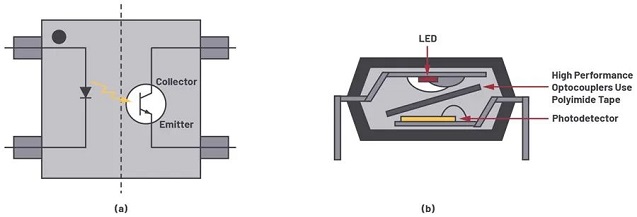
Figure 1. (a) Schematic Diagram of the Optocoupler, (b) Cross-Sectional View of the Optocoupler Package.
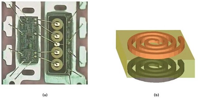
Figure 2. (a) Digital Isolator in Plastic Package, (b) Transformer Cross-Section.
Ⅰ. Digital isolators use polyimide film
Polyimides are a type of polymer made up of imine monomers. Many digital isolators use polyimide as an insulating material for a variety of reasons, including its high breakdown strength, thermal and mechanical stability, chemical resistance, ESD performance, and low dielectric constant. Polyimide has outstanding ESD performance, able to survive EOS and ESD events in excess of 15 kV in addition to its good high voltage performance. The polyimide polymer absorbs some of the charge during an energy-limited ESD event, creating stable free radicals that stop the avalanche process and remove some of the charge. Other dielectric materials, such as oxides, do not often have this ESD tolerance, and avalanches can develop even at low ESD energy when the ESD level surpasses the dielectric strength. Polyimide also exhibits great thermal and mechanical stability, with a weight loss temperature of over 500°C and a glass transition temperature of over 260°C, tensile strength of over 120 MPa and an elastic elongation of over 30%. Despite its great elongation, polyimide has Young's modulus of roughly 3.3 GPa, making it difficult to deform.
One of the reasons polyimide is extensively utilized as an insulating layer for high-voltage cables is its superior chemical resistance. Polyimide films may be coated on semiconductor wafer substrates, and their exceptional chemical resistance makes IC manufacturing, such as the Au plating needed to manufacture iCoupler® transformer coils, easier. Finally, to reduce the capacitance of the isolation barrier, a thick polyimide sheet with a dielectric constant of 3.3 works well with tiny diameter Au transformer coils. The capacitance between the input and output of most iCoupler products is less than 2.5 pF. Polyimide is increasingly employed in microelectronics applications due to these qualities, and it is a suitable insulating material for iCoupler's high-voltage digital isolators.
Ⅱ. Construction and fabrication of digital isolators
The digital isolator is made up of three basic components: an isolation barrier coupling element, an insulating substance, and a modulation and demodulation circuit for signal transmission. The insulating material is utilized to allow the isolation barrier to achieve a given level of isolation, which is primarily determined by the dielectric strength and thickness of the barrier. Organic dielectric materials, such as polyimide, and inorganic dielectric materials, such as silicon dioxide or silicon nitride, are the two basic categories of dielectric materials. Dielectric strengths of oxides and nitrides range from 700 V/m to 1000 V/m. However, due to their tremendous stress, reliable creation of 15 m to 20 m thick films on large-scale current IC wafers is impossible. Organic films are very susceptible to ESD, and even minor voltage overstresses can cause catastrophic avalanche disintegration. Organic films, such as polyimide, are made up of very long CH chains, and a modest energy-limited ESD event can damage some local CH chains without compromising the material's structural integrity, resulting in higher ESD resistance. Tolerance. Polyimide has a lower dielectric strength than oxide or nitride, ranging from 600 V/m to 800 V/m. However, because of the film's low stress, thicker polyimide layers of 40 m to 60 m can be created without incurring significant costs.The withstand voltage range of the 30 m polyimide film is 18 kV to 24 kV, which is superior than the 20 m oxide film (14 kV to 20 kV). Polyimide-based isolators are an excellent alternative for applications that require high resist voltages against impulse voltages like those seen in lightning strikes.
Photoresists are commercially available polyimide films that are deposited on wafers at precise thicknesses and subsequently patterned using typical photolithographic methods. Figure 3 depicts the isolation transformer's process flow in digital isolators. The bottom coil is made by spin-coating a first layer of photosensitive polyimide on the CMOS wafer, with the top metal layer creating the top coil, and the polyimide layer is formed by photolithography. To attain good structural quality, the polyimide is subsequently thermally cured. To produce the top coil package, the top coil layer is electroplated, then a second polyimide layer is placed, shaped, and hardened. Because there are no voids in the deposited polyimide film (as shown in Figure 4), there is no corona discharge, therefore the transformer equipment has good aging characteristics and is well suited to continuous AC or DC voltage operation.

Figure 3. Industrial Flow Diagram of an Isolation Transformer.
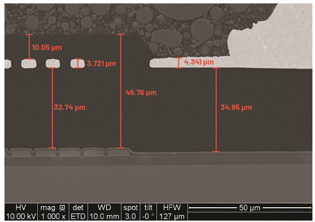
Figure 4. Cross-Sectional View of Fabricated Isolation Transformer
Ⅲ. High Voltage Performance for Digital Isolators
The maximum tolerate voltage for a length of one minute determines the UL 1577 isolation rating. The digital isolator is tested for 1 second at 120 percent of its rated voltage during factory testing. The factory test setting for a 2.5 kV rms 1 min rated digital isolator is 1 second at 3 kV rms. There are two crucial high-pressure performance factors to be mindful of in practical applications. The maximum working voltage at which the insulation must remain intact during continuous AC or DC operation is one example. According to VDE 0884-11, an isolator providing reinforced isolation must have a life of more than 37.5 years at a 1 ppm failure rate at 120 percent of the rated voltage.If a reinforced digital isolator is rated to function at 1 kV rms, its lifetime at 1.2 kV rms must be larger than 37.5 years, assuming a 1 ppm failure rate. Similarly, an isolator providing basic insulation must have a life of more than 26 years at 120 percent of the rated voltage and a failure rate of 1000 ppm. The greatest transient isolation voltage that the device can withstand is another significant application parameter. Waveforms for transient tests can vary; Figure 5 displays an example waveform based on EN 60747-5-5 or IEC 61010-1. The time it took to move from 10% to 90% was around 1.2 seconds, and the time it took to go from peak to 50% was 50 seconds. This is to imitate lightning strike conditions, thus the isolator's surge performance must be powerful enough to match field standards. ESD tolerance is a critical feature of semiconductor devices, and the device's high spike performance indicates that it has strong ESD tolerance.
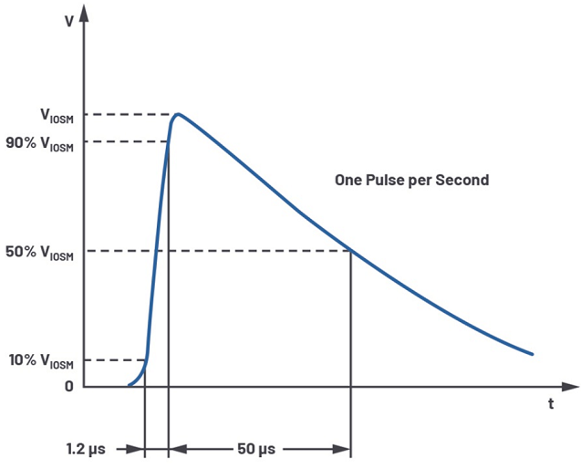
Figure 5. IEC 61010-1 Surge Test Waveform
Ⅳ. Properties of Polyimide Films
On the one hand, the DC bulk conductivity of polyimide is very low in the electric field range of 40 V/m, about 10 -16, and stays very low at least up to 150 V/m, as shown in Figure 6. The AC breakdown electric field value of the polyimide film, on the other hand, reaches a minimum of 450 V rms/m at 60 Hz. Spin-coated polyimide films are an ideal insulating material for reliable digital isolator applications because of all of these qualities.
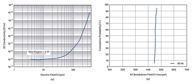
Figure 6. The Main Electrical Properties of the Spin-Coated Polyimide Film Itself Measured at the Wafer Leve-(A) DC Conductivity Versus Electric Field, (b) AC Breakdown Electric Field Distribution.
Figure 7 demonstrates the surge performance of an isolator with a polyimide film thickness of 30 m. Surge tests up to 18 kV will pass these isolators, with a first failure voltage of 19 kV for negative pulses and 20 kV for positive pulses.
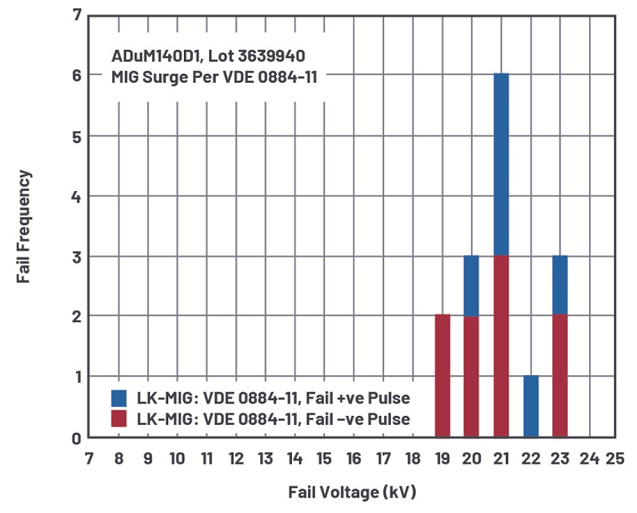
Figure 7. Surge Performance of Isolator with 30 μm Thick Polyimide Film
Ⅴ. Aging of polyimide film
High-pressure endurance tests are used to investigate the service life of polyimide. Given enough time and voltage, any insulator can fail. Figure 8 depicts a typical configuration. Different high voltages are given to groups of devices from a high voltage power source, and switching/measuring devices (such as an Agilent 34980 and a computer) are used to monitor when these devices fail. The process of dismantling these devices might take anywhere from days to months.

Figure 8. Experimental Setup for High Voltage Endurance Testing.
A Weibull chart, as shown in Figure 9, can be used to study the time distribution of device failures. When six different voltages were applied to groups of 16 devices, each group produced a lovely Weibull graphic. The mean time to failure (MTTF), or the time to failure at a given failure rate, can be calculated using the Weibull plot (eg 1 ppm). At high pressure, the time to failure is clearly shorter than at low pressure. According to VDE 0884-11, the minimum to maximum MTTF must span at least two orders of magnitude, with 63 percent of failure durations exceeding 1E7 seconds (about 116 days) at the lowest test voltage. Figure 9 shows that the datasets generated at these 6 voltages meet these requirements.
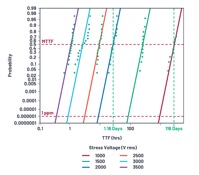
Figure 9. Weibull Profile of an Isolator with a 20 μm Thick Polyimide Layer.
The time to failure is depicted depending on the stress voltage to deduce the operational voltage. The working voltage for basic insulation is established by reducing the voltage by 20%, resulting in a time to failure or service life of more than 24 years at 1000 ppm. Similarly, the operating voltage for reinforced insulation is established by derating the voltage by 20%, resulting in a service life of more than 30 years at 1 ppm. The fundamental mechanism of breakdown is charge injection, which occurs when electrons from the electrodes collide directly with the polyimide surface area. When charges are injected into the polyimide surface under HVAC conditions, the breakdown process commences. Charges can build up at specific accumulation sites on the surface. The electrical energy is released when it has accumulated, and the stored electrostatic energy might generate stress in the local mechanism. This strain eventually generates local free volumes (voids or microcracks) through the quantum activation process, resulting in more local accumulation points. This process will result in a constant loss in insulating capacity and eventual breakdown by electrical breakdown if the HVAC persists long enough.
The service life L can be represented as Equation 1 using thermodynamic analysis, where Et is the threshold field at which no charge injection occurs and m and n are proportionality constants.
We used the approach outlined in ANSI /IEEE Standard 930-1987 to assess the HVAC withstand data for iCoupler devices. ("IEEE Guide for Statistical Analysis of Electrical Insulation Voltage Endurance Data"), resulting in:
Because the thermodynamic model does not define a threshold field, this phenomenological fit is utilized to derive the shortest lifetime, as illustrated in Equation 2. If we try to measure the threshold field, the HV test will take a lengthy time. In Figure 10, we utilize Equation 2 to simulate the failure time. As you can see, the model closely resembles the facts.
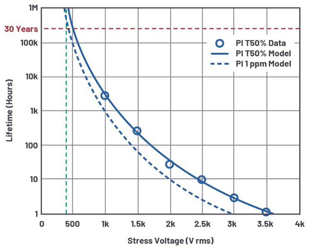
Figure 10. Failure Time Diagram for an Isolator with a 20 μm Thick Polyimide Layer.
We also discovered that the lifetime of iCoupler devices at DC or unipolar AC voltages is at least two orders of magnitude longer than at bipolar AC voltages. As seen in Figure 11, the accumulated charge around the electrode generates an internal field barrier zone, further inhibiting charge injection into the polyimide layer. The reversal of the electric field in bipolar AC waveforms precludes the establishment of this stable field barrier, and the accumulation area continues to invade the polyimide layer, finally causing electrical breakdown. SiO2 has a lower lifespan when exposed to DC or unipolar AC energy.
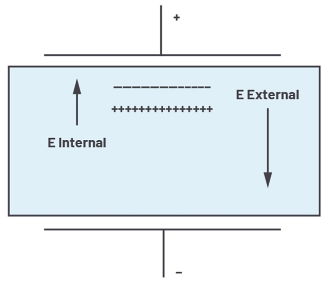
Figure 11. Field Barrier Region with Accumulated Charge Resulting in a Zero Net Electric Field.
Figure 10 shows lives based on worst-case bipolar AC waveforms. The HV lifespan is even longer for unipolar AC or DC waveforms. This paper's model is for polyimide insulation, not for insulators with SiO2 insulators as the major means of isolation. Similarly, the models used to forecast the HV lifetime of SiO-based digital isolators are unaffected by isolation systems based on polyimide.
The lifetime of polyimide sheets at unipolar and bipolar voltages is compared in Figure 12. It can be shown that the peak stress voltage of the unipolar voltage is twice that of the AC bipolar voltage at the same fault time. Fundamentally, the lifetime is determined by the peak-to-peak voltage of the polyimide film, not its peak stress voltage.
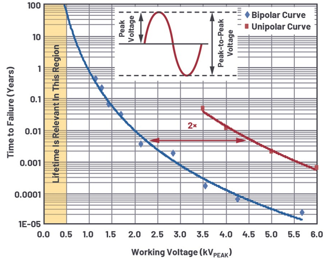
Figure 12. Time-to-Failure Comparison between AC Bipolar Voltage and Unipolar Voltage.
Ⅵ. Structure Improvement of Polyimide Film
The charge injection barrier depicted in FIG. 13 can be employed to improve polyimide's high voltage resistance. It is better to utilize oxides or nitrides with large band gaps and high dielectric constants for the charge injection barrier. A big band gap can enhance the electrical barrier to charge injection, whereas a high dielectric constant helps minimize the electric field near the electrodes.

Figure 13. (a) Transformer Isolation without and (b) with Nitride Charge Injection Barrier.
A band diagram, as shown in Figure 14, can be used to analyze charge injection for a given isolated system. Figure 13 depicts the four key materials employed in the isolation system: Au for the top coil, polyimide for isolation between the top and bottom coils, oxide as a charge injection barrier, and TiW as the seed crystal beneath the Au layer. The quantity of charge injected by Au or TiW into polyimide, oxide (electrons), or holes can be determined using the band diagram.
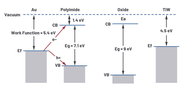
Figure 14. Band Diagram of Charge Injection.
The measured charge current versus time for polyimide and polyimide with SiN implant barrier at 1000 V is shown in Figure 15. When polyimide with SiN barrier was used instead of polyimide alone, steady-state current was reduced by more than 5 times. This reveals a significant reduction in the charge injection process, which is known to be a primary contributor to electrical aging in high-voltage environments.
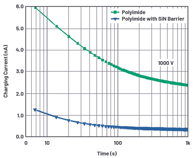
Figure 15. Comparison of Charging Current (at 1 kV) for Polyimide and Polyimide with SiN Implanted Barrier.
Figure 16 illustrates the time to failure (HVE test) versus applied AC voltage at 60 Hz, 1 kV rms to 3.5 kV rms for single-die configurations with polyimide and with polyimide/SiN barrier for single-die configurations with polyimide and with polyimide/SiN barrier. The lifetime is shown at 50% and the projected values for the dataset are shown at 1 ppm on the graph. In addition, the operating voltage (supposedly) at a lifetime of 30 years is stated in both circumstances. Improved digital isolators with SiN injection barriers run at >900 V rms, while digital isolators with polyimide insulation operate at 400 V rms (750 V at 1 ppm with 20 percent derating ). These thin SiN layers limit bipolar charge injection at the start of space charge generation, resulting in lower current flow, less thermal effects, and (presumably) a longer lifetime at a given voltage.
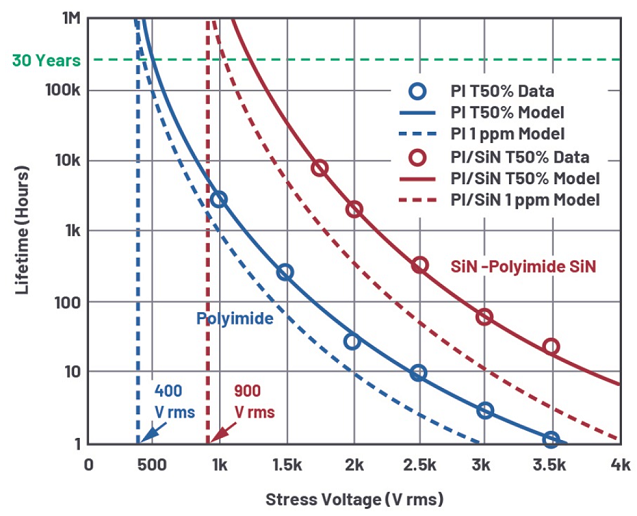
Figure 16. Comparison of Failure Time of Polyimide Isolators with and without SiN Charge Injection Barrier
Ⅶ. Summary
Polyimide films have outstanding high voltage performance, from surge voltage to high voltage withstand. We discovered that by adopting charge injection barriers with large dielectric constants and large band gaps, the anti-aging characteristics of these films can be further increased. The usage of polyimide films in digital isolators is described in this article, and they are a good choice for producing isolation barriers for digital isolators.
 What is a Great Choice for Digital Isolators to Build Isolation Barriers?UTMEL31 March 20224814
Hello everyone, I am Rose. Welcome to the new post today. A digital isolator is a chip that has high resistance isolation characteristics when digital signals and analog signals are transmitted in an electronic system to realize the isolation between the electronic system and the user. and capacitive isolation to achieve.
Read More How to Select a Digital Isolator?UTMEL12 April 20216477
A digital isolator is a chip used to make the electronic system have high resistance isolation when signals and analog signals are transmitted, so as to realize the isolation between the electronic system and its users. The reason why designers introduce isolation is to meet safety regulations or reduce ground loop noise.
Read More Vibration Isolator: Types and ApplicationsUTMEL13 January 202112137
A vibration isolator is an elastic element connecting equipment and foundation to reduce and eliminate the vibration force transmitted from the equipment to the foundation and the vibration transmitted from the foundation to the equipment. This article will introduce some of the types of vibration isolators and their applications to you.
Read More What is An Optoisolator?UTMEL09 January 20217585
An optoisolator, also called optical coupler, optocoupler, and opto-isolator, is a device that encapsulates the infrared light-emitting device, the infrared light receiving device, and the signal processing circuit in the same tube socket.
Read More
Subscribe to Utmel !


 Product
 Brand
Brand Articles
 Tools
Tools


