Product
 Brand
Brand Articles
 Tools
Tools
The Through Hole of the PCB Circuit Board Must be Plugged, Why?
What is a PCB Via? | PCB Knowledge
Electrical hole Conduction hole is another name for a via hole. The circuit board through hole needs to be plugged in order to satisfy client requirements. The standard aluminum sheet plugging procedure is changed after a lot of practice, and the circuit board surface is finished with a hole made of white mesh. Both the production and the quality are dependable.

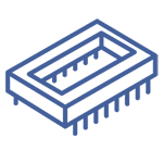
Figure. 1
The connectivity and conductivity of wires are facilitated via through holes. Higher standards for printed board manufacturing technology and surface mount technology are also put forth by the development of the electronics sector, which also encourages PCB development. The process of plugging a via hole was created, and concurrent fulfillment of the following conditions was mandated:
The following conditions must be met: (1) There must be only enough copper in the via hole, and the solder mask may or may not be plugged; (2) There must be tin-lead in the via hole, with a minimum thickness requirement of 4 microns; (3) The via holes must have solder resist ink plug holes, be opaque, and be free of tin rings, tin beads, and flatness.

Figure. 2
As electronic goods move in the direction of being "light, thin, short, and compact," PCBs are also moving in that way. As a result, there are many SMT and BGA PCBs, and customers need plug holes when installing components. Five features:
(1) Prevent short circuits brought on by tin piercing through the component surface through the through hole while the PCB is over wave soldering. This is especially important when the via hole is placed on a BGA pad because doing so will make it easier to solder BGAs.
(2)Avoid leaving flux residues in the through holes.
(3)Lastly, the PCB needs to be vacuumed on the testing machine to create a negative pressure before it is finished after the surface mounting and component assembly of the electronics factory.
(4Prevent tin beads from popping out during wave soldering, which could lead to short circuits.
(5)Prevent solder paste on the surface from pouring into the hole to create false soldering and alter placement.
Conductive hole plug technology is now available.
In order to satisfy customers, via hole plug holes for surface mount boards, particularly those for BGA and IC mounting, must be flat with a bump of plus or minus 1 mil and must not have red tin on the edge of the via hole. Tin beads are concealed in the via hole. The via hole plug hole technology can be characterized as variable, with a very long process flow and challenging process control, according to the requirements of the requirements. Problems include oil loss during hot air leveling and green oil solder resistance tests, as well as oil explosion following curing, frequently occur. Different PCB plugging procedures are compared, elaborated on, and their benefits and drawbacks are discussed in accordance with the real production conditions:
As a surface treatment technique for printed circuit boards, hot air leveling works by using hot air to remove excess solder from the printed circuit board's surface and from the board's holes while evenly applying the remaining solder to the pads, non-resisting solder lines, and surface packaging points. one.
1. After hot air leveling, plug the opening.
Board surface solder mask, HAL, plug hole, and curing make up the process flow. After hot air leveling, the through hole plug holes of all the customer-required fortresses are completed using the non-plug hole method and an aluminum sheet screen or an ink blocking screen. The ink used for plugging can be thermosetting or photosensitive. It is preferable to use the same ink as the board surface for the plugging ink in order to maintain the same color of the wet film. This procedure can prevent the via hole from dripping oil after hot air leveling, but it is simple to make the board surface contaminated and uneven by plugging ink. Customers can easily place virtual solder (especially in BGA) without intending to. Such a large number of clients reject this approach.
2. The front plug hole operation using hot air
2.1 Cover the holes with aluminum sheet, let it harden, and then grind the plate to transfer the design.
To create a screen, an aluminum sheet is drilled out using a CNC drilling machine, and the hole is then filled to make sure the via hole is completely filled. Thermosetting ink, which must have a high hardness, can also be used for plugging. Little shrinkage occurs in the resin, and there is good adhesion to the hole wall. Pretreatment, plug hole, grinding plate, pattern transfer, etching, and solder mask on the board surface make up the process flow.
Through-hole plug holes can be made flat with this technique, and hot air leveling won't lead to issues with product quality like oil explosion and oil droplets at the hole's edge. But in order for the copper thickness of the hole wall to match the customer's specification, this method calls for a one-time thickening of copper. To ensure that the resin on the copper surface is entirely removed and that the copper surface is clean and pollution-free, extremely high standards for copper plating on the entire board and extremely high standards for grinding machine performance must be met. Since many PCB companies lack a one-time copper thickening process and the equipment's performance cannot match the standards, this procedure is not frequently employed in PCB factories.
2.2 After using aluminum sheets to cover holes, immediately screen-print the solder mask on the board's surface.
The aluminum sheet that needs to be plugged in order to create a screen is cut out using a CNC drilling machine, installed on the screen printing machine for plugging, and stopped for no longer than 30 minutes after plugging is finished. Directly screen the solder on the board using a 36T screen. The procedure follows: pre-treatment, silk screen, plugging, pre-baking, exposure, and development - healing
This procedure may guarantee that the plug hole is smooth, the oil on the via hole cover is good, and the wet film's color is constant. Poor solderability is caused by the pad; following hot air leveling, the via hole's edge foams and loses oil. This kind of production control is challenging. To guarantee the quality of plug holes, process engineers need to employ specific procedures and guidelines.
2.3 The board surface is soldered once the aluminum sheet's holes have been filled, the board has been developed, pre-cured, and ground.
The aluminum sheet that needs a plug hole to create a screen is drilled out using a CNC drilling machine, installed on the shift screen printing machine for the plug hole, and then the plate is ground for surface treatment after the plate has been allowed to cure. The plug hole needs to be full and preferably protrudes on both sides. Pre-treatment - plug hole is the order of the process. board surface solder mask - pre-baking - development - pre-curing
Since this procedure uses plug hole curing to ensure that the via hole does not leak oil or explode after HAL, many customers do not accept it because after HAL, it is challenging to fully resolve the buried tin beads in the via hole and the tin on the via hole.
2.4 Both the plug hole and the board's solder mask are finished at the same time.
Using a backing plate or a nail bed, a 36T (43T) screen is put on the screen printing machine, and all the via holes are sealed up while finishing the board surface. Preprocessing, silk screen, prebaking, exposure, development, and curing make up the process flow.
The equipment is utilized at a fast rate during this quick process. After hot air leveling, the air expands and penetrates the solder mask, creating voids and unevenness. This can prevent the via hole from dropping oil or becoming filled with tin. In the hot air leveling, a few through holes will be concealed. Following extensive testing, our business has chosen several ink types and viscosities, adjusted the silk screen pressure, etc., essentially resolving the via hole and unevenness, and adopted this method for mass production.
 UTMEL
UTMEL
We are the professional distributor of electronic components, providing a large variety of products to save you a lot of time, effort, and cost with our efficient self-customized service. careful order preparation fast delivery service
How to solve the redness of the opening of the PCB via hole?
Because when you plug the VIA hole, the plug is not full enough. After printing the surface ink, the ink flows into the hole, resulting in the thinning of the ink around the hole.
What is the role of many small metal holes on the PCB?
"Via Hole", that is, a through hole, refers to a hole on a multilayer circuit board that is only used for conductive interconnection between layers, and is generally no longer used for plug-in soldering of component feet. This type of hole is plated with a layer of copper in the hole through the "copper sinking" process to conduct electricity.
How to do PCB via hole layout?
(1) Avoid setting via holes within or within 0.6mm of surface mount pads. (2) Component pads without external pins (such as chip resistors and capacitors, adjustable potentiometers and capacitors, etc.), no through holes are allowed between the pads (that is, no via holes are opened under the components; if used Solder mask blocking can be excluded) to ensure cleaning quality. (3) As the via holes for test support, when designing the layout, it is necessary to fully consider the minimum spacing of probes with different diameters for automatic online testing. (4) The matching gap between the via hole diameter and the component lead is too large to cause false welding. Generally, the diameter of the conduction hole is 0.05-0.2mm larger than the diameter of the lead wire, and when the diameter of the pad is 2.5-3 times the diameter of the conduction hole, it is easy to form a qualified solder joint. (5) The via hole and the pad cannot be connected to avoid solder loss or thermal isolation. If the via hole really needs to be connected to the pad, it should be interconnected with a thin line (less than 1/2 of the pad width or 0.3mm~0.4mm) as much as possible, and the distance between the via hole and the edge of the pad is greater than 1mm
 Pull-Down Circuit Guide: Working Principle, Resistor Value, Circuit Design, and ApplicationsUTMEL26 June 2026168
Learn how pull-down circuits work, how to choose a pull-down resistor value, and how to design reliable microcontroller inputs, MOSFET gates, reset pins, and sensor interfaces.
Read More HF PCB Circuit Design 10 QuestionsUTMEL16 March 20225352
Hello everyone, I am Rose. Today I want to give you a full explanation about PCB design. I Hope the following ten questions will give you a satisfied answer.
Read More How Many do You Know About the 12 Components Included in the Circuit Board?UTMEL12 February 20228852
We are lucky to live in an era where electronic devices are readily available. These electronic devices, on the other hand, come to us thanks to the incredible components on the circuit board, and we frequently wonder what makes electronic devices operate, how they achieve such massive success, and how they accomplish it. Electronic devices are incredible things; you can't see what's going on within them, but you can see what they're capable of. We'll talk about the wonders of PCBs and how to get past them to construct the circuit board in this article.
Read More![50 Frequently Asked Questions about PCB Layout [Q&A]](https://res.utmel.com/Images/Article/b5ce2a0a-d37c-4243-aff3-df7b2da2db0f.jpg "50 Frequently Asked Questions about PCB Layout [Q&A]") 50 Frequently Asked Questions about PCB Layout [Q&A]UTMEL16 November 20217172
50 Frequently Asked Questions about PCB Layout [Q&A]UTMEL16 November 20217172In the design of electronic products, PCB layout and routing is an important step, and the quality of PCB layout and routing will directly affect the performance of the circuit.
Read More An Overview of Development BoardUTMEL18 December 202515409
The development board is a circuit board used for embedded system development. Development boards are generally customized by embedded system developers according to development needs.
Read More
Subscribe to Utmel !
![AME25-9SJZ-ST]() AME25-9SJZ-ST
AME25-9SJZ-STAimtec
![AMEL20-3.3SCJZ-ST]() AMEL20-3.3SCJZ-ST
AMEL20-3.3SCJZ-STAimtec
![X1024S03/T]() X1024S03/T
X1024S03/TTDK
![X1024S03/N]() X1024S03/N
X1024S03/NTDK
![X1548S03]() X1548S03
X1548S03TDK
![30725]() 30725
307253M
![BXA10-48S05]() BXA10-48S05
BXA10-48S05IXYS
![VRB2424S-6WR3]() VRB2424S-6WR3
VRB2424S-6WR3MORNSUN
![X1548S12/NT2]() X1548S12/NT2
X1548S12/NT2TDK
![X1548S02/PT2]() X1548S02/PT2
X1548S02/PT2TDK