Revolutionizing the Electric Vehicle Industry with Silicon Carbide
Overview: This article provides applications of silicon carbide devices in power electronics. It also highlights the challenges associated with paralleling SiC MOSFETs and the need for a thorough examination of the current imbalance mechanism.
The market for electric vehicles (EVs) is expected to continue growing rapidly over the next two decades, prompting rapid development in silicon carbide (SiC) and metal oxide semiconductor field effect transistor (MOSFET) devices over the past decade.
Ⅰ. Merits of Silicon Carbide
Due to their low device losses, high system efficiency, and, most importantly, lower vehicle level cost, SiC MOSFETs are seen as a preferred option in the EV powertrain inverter application by the automobile industry. SiC MOSFET technology is expected to see massive investment, rapid technology development, and significant further cost reduction over the next 5–10 years as the automotive market expands.
Other industrial markets, such as photovoltaic, energy storage, charging infrastructure, traction, and the power grid, also anticipate a high level of market penetration of SiC devices as a result of technological advancements and price reductions. Fast switching speed, high operating temperature, high breakdown voltage, and linear current-voltage (I-V) properties are just a few of the device advantages that set SiC MOSFETs apart from their silicon (Si) insulated-gate bipolar transistor (IGBT) counterparts.
Both the properties of the SiC material and the structure of the unipolar MOSFET contribute to the superiority of these devices. The SiC wide band gap (WBG) material property makes higher temperature operation and a larger critical electric field possible. The automobile industry is currently driving the highest operation junction temperature from 175°C to 200°C, a temperature limit that is not limited by SiC material but rather by the mosfet gate oxide dependability.
The lower specific resistance in the drift region is a result of the higher doping concentration and thinner drift layer made possible by the higher critical electric field of SiC material. Therefore, a 1.2 or 1.7 kV unipolar mosfet device can be easily achieved with SiC material, but due to the high specific resistance of the drift region, it is quite difficult with Si material. For Si IGBTs, the Si wafer thickness is roughly 10 times greater than that of SiC MOSFETs (up to 1.7 kV), which have an epitaxial layer thickness of approximately 1 μm/100 V.
When compared to the bipolar IGBT structure, the unipolar mosfet's fast switching speed and linear I-V property are advantageous to conduction losses under low loads. The elimination of tail current in unipolar MOSFETs also contributes to their lower switching loss when compared to bipolar IGBTs.
Ⅱ. What is preventing the widespread adoption of SiC MOSFETs in industry?
SiC MOSFETs have a number of advantages over competing devices, but there are still a number of barriers preventing their widespread commercial use. In terms of material defects such as micro-pipes, dislocations, and stacking faults, in both SiC substrates and epitaxy, which affect the quality, they have yet to be fully resolved. SiC device properties, yield, and single-chip device size are all affected by the presence of material defects.
A larger inconsistency in SiC device parameters is also caused by the immaturity of manufacturing equipment, processes, and device design for SiC devices. Gate oxide reliability and threshold voltage (Vth) instability are two device-level issues that SiC MOSFETs are still working to solve. The high sensitivity to circuit parasitics that results from the fast switching speed presents new challenges for the designers of SiC power semiconductor packaging, gate drivers, and power loop circuits.
For the high-current application of SiC MOSFETs, the current imbalance among the paralleled SiC MOSFETs has been a practical problem in addition to the immaturity of the SiC material, device parameter inconsistency, and fast switching speed. Under typical operating conditions, the current imbalance may result in a thermal imbalance and raise issues with long-term reliability.
The design margin is typically set to a high level to avoid significant excessive stress on a single device as a result of the current imbalance, but this results in less utilization of the device's full potential and a higher cost. There has been a rise in the amount of research done over the past decade to address the difficulties of paralleling SiC mosfets. The research can be broken down into two distinct areas: (1) an examination of the current imbalance mechanism and (2) an examination of the current sharing methodologies.
Ⅲ. Paralleling SiC MOSFETs
Power semiconductors are frequently used in parallel at a variety of levels. Thousands of semiconductor unit cells make up a SiC MOSFET chip at the die level, all of which are connected in parallel through the drain and source metallization layers and gate runners. Power semiconductor dies in multichip power modules or discrete devices are often run in parallel to achieve a high current rating in high-power applications.
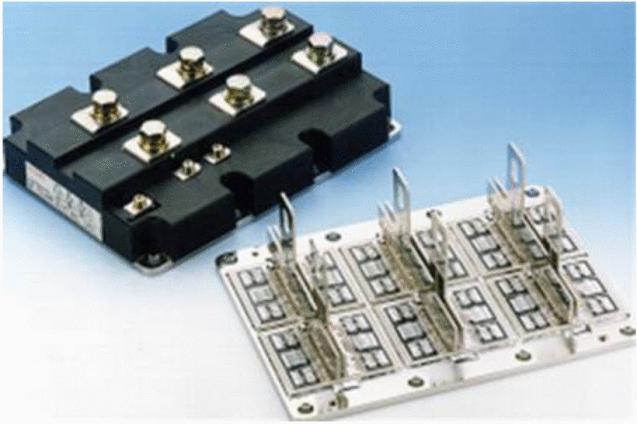
For example, the power module in Fig. 1 has a current rating of 3600 A and has 24 IGBT chips and 12 diode chips connected in parallel. Parallel connection of multiple power modules is also used at the circuit level to achieve the required current level in some high-current and high-power applications.

Fig. 1. IGBT-high-current-module with paralleled IGBTs and diodes. Source: IEEE Transactions on Power Electronics
Ⅳ. Productivity Boosting Effects of Die Size
Fabricating a larger die is preferred when increasing a power device's current rating. However, there are a few obstacles that prevent the die size from growing any larger. Die size and yield are inversely proportional. Larger die sizes typically have lower yields, leading to higher costs per amp due to SiC material defects and process imperfections.
Making a large die for a SiC MOSFET is more difficult than doing so for a Si IGBT. Due to their material properties, both the SiC substrate and epitaxial material are more prone to higher-level defects. In addition, the technology for equipment manufacturing and process control used to make SiC MOSFETs is not as refined as that used to make Si IGBTs.
At the moment, the highest current rating of a single IGBT chip with a die size of 10 x 12 ![]() for Si IGBTs with lower voltages (≤750 V) is around 300 A. While the highest current rating of a single SiC mosfet die with a 5 x 5
for Si IGBTs with lower voltages (≤750 V) is around 300 A. While the highest current rating of a single SiC mosfet die with a 5 x 5 ![]() die size is about 100 A for SiC mosfets with the same voltage level.
die size is about 100 A for SiC mosfets with the same voltage level.
When using SiC MOSFETs, the level of device electrical parameter variations among the paralleled chips can increase due to the greater number of dies connected in parallel. There is a heightened potential for current imbalance as a result.
Ⅴ. Impact of Less Maturity in Paralleling SiC
Low yield and greater variance in device parameters are two problems caused by the immaturity of the SiC MOSFET manufacturing process, which is another obstacle to paralleling SiC MOSFETs. High variation limits of the chip's characteristics are specified in SiC mosfet datasheets. Inconsistent device properties, such as on-resistance (![]() ), transconductance (
), transconductance (![]() ), and
), and ![]() , could cause an uneven flow of current during steady state and switching transients.
, could cause an uneven flow of current during steady state and switching transients.
Ⅵ. Role of Switching Speed
It is not enough to simply address the issues of small die size and variable device parameters; the fast switching speed associated with the unipolar MOSFET structure also requires special care. Due to its interaction with the parasitic inductance, rapid switching causes ringing, overshoot, and false-triggering, making it highly sensitive to parasitic parameters.
Ⅶ. Reason for the Current Imbalance
The highly interdisciplinary nature of multichip power module design presents yet another difficulty. It is common for the "optimal" design solution to be the result of compromises among competing criteria, such as those pertaining to electrical, mechanical, thermal, environmental, reliability, and manufacturability.
The overarching design principles from various perspectives are often in conflict with one another. For better thermal performance, for instance, a larger distance between paralleled chips is desired, but a smaller distance is preferred for improved electrical performance.
The electrical, thermal, and mechanical performances are highly coupled, and this is in addition to the tradeoffs introduced by the various design principles. Mismatched thermal distribution, mechanical performance, and ultimately reliability issues can result from a current imbalance between paralleled power devices.
As a result, the current imbalance among the paralleled dies cannot be optimally corrected by any single solution. Before taking steps to correct the current imbalance, a thorough examination of its causes is required.
Ⅷ. Summarizing the Key Points
● Silicon carbide MOSFET devices have low device losses, high system efficiency, and lower vehicle level costs, making them a preferred option in the electric vehicle powertrain inverter application by the automobile industry.
● The market for electric vehicles is expected to continue growing rapidly over the next two decades, prompting rapid development in SiC MOSFET devices over the past decade.
● The electrical, thermal, and mechanical performances of SiC MOSFETs are highly coupled, and a thorough examination of the current imbalance mechanism is required before taking steps to correct it.
● The current imbalance among paralleled SiC MOSFETs cannot be optimally corrected by any single solution, and a thorough examination of its causes is required.
● SiC MOSFET technology is expected to see massive investment, rapid technology development, and significant further cost reduction over the next 5-10 years as the automotive market expands.
Ⅸ. Reference
Li, Helong, Shuang Zhao, Xiongfei Wang, Lijian Ding, and Homer Alan Mantooth. “Parallel Connection of Silicon Carbide MOSFETs—Challenges, Mechanism, and Solutions.” IEEE Transactions on Power Electronics 38, no. 8 (August 2023): 9731–49. https://doi.org/10.1109/tpel.2023.3278270.
 Modeling Wide Band-Gap Semiconductors for Enhanced PerformanceRakesh Kumar, Ph.D.31 January 20243464
The article delves into the challenges faced by silicon-based power electronic devices and highlights the potential of wide band-gap semiconductors. It also emphasizes the importance of modeling power semiconductor devices and provides insights into various models. For electrical energy conversion to be dependable and effective, power electronics and semiconductor device technologies are essential.
Read More Optimizing Energy Management with Non-Isolated DC-DC ConvertersRakesh Kumar, Ph.D.04 February 20243107
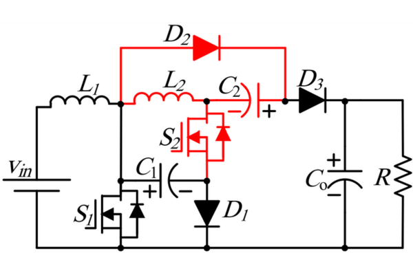
The article classifies DC-DC converters and discusses the benefits and limitations of them. It proposes a modified DC-DC converter topology that combines the Cuk and Positive Output Super Lift Luo topologies to achieve a higher voltage gain with fewer components.
Read More ‘6G Networks’ - Pioneering the Next Era of Connectivity And InnovationRakesh Kumar, Ph.D.18 March 20243449
The article provides a comprehensive overview of the evolving landscape of mobile networks, the requirements that will shape the future of mobile communication, and the innovative technologies driving the transition to 6G.
Read More Review of IoT-Based Smart Home Security Systems- Part 1Rakesh Kumar, Ph.D.28 March 20243807
The article discusses the evolution of IoT-based smart home security systems, integrating advanced technologies like Raspberry Pi, PIR sensors, and voice recognition for enhanced user experience and efficiency.
Read More Understanding Photodiodes: Working Principles and Applications - Part 2Rakesh Kumar, Ph.D.24 May 20244817
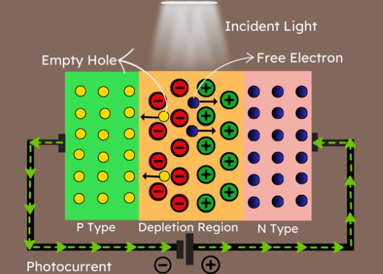
The article provides a comprehensive overview of photodiodes, focusing on their operational principles, key factors affecting their efficiency, advantages, and disadvantages, and highlights their diverse applications.
Read More
Subscribe to Utmel !
![T0051388799]() T0051388799
T0051388799Apex Tool Group
![T0051387299]() T0051387299
T0051387299Apex Tool Group
![T0051386099]() T0051386099
T0051386099Apex Tool Group
![T0051388599]() T0051388599
T0051388599Apex Tool Group
![T0051388099]() T0051388099
T0051388099Apex Tool Group
![T0051387499]() T0051387499
T0051387499Apex Tool Group
![T0051387099]() T0051387099
T0051387099Apex Tool Group
![T0051388299]() T0051388299
T0051388299Apex Tool Group
![83-6337-0027]() 83-6337-0027
83-6337-0027NTE Electronics, Inc.
![83-1001-8010]() 83-1001-8010
83-1001-8010NTE Electronics, Inc.


 Product
 Brand
Brand Articles
 Tools
Tools


