
 Product
 Brand
Brand Articles
 Tools
Tools
An Overview of JFET

JFET: Construction and Working Explained
Catalog
Ⅰ Basics of JFET
A transistor is a linear semiconductor component that regulates the current by applying an electrical signal of lesser power. Transistors can be classified into approximately two main divisions: bipolar and field-effect.
For electronics circuits, the junction field-effect transistor or JFET is commonly used. The junction field-effect transistor is a versatile and useful electronic device and can easily be used in a number of electronic circuits, from JFET amplifiers to JFET transfer circuits.
Junction field-effect transistor is available free of charge, and JFETs can be purchased for very little money. This makes them perfect for use in many circuits where you are interested in a strong balance between cost and efficiency.

JFET and circuit symbol
JFETs have been around for many years, and although they do not deliver the MOSFET's exceptionally high DC input resistance, they are nonetheless very reliable, durable, and easy to use. This makes those electronic components an ideal choice for many designs of electronic circuits. The modules are also available in both leaded system and surface mount configurations.
JFET is an integral feature for analog electronic controls controlled by precision level voltage. We can use JFET as a voltage controlled resistor or as a switch, or even use the JFET to make an amplifier. Replacing the BJTs, it is also an energy-friendly variant. JFET provides low power consumption and relatively low heat dissipation, thereby improving the overall circuit performance. This also has very high current impedance and is a major benefit over BJTs.
There are different types of transistors, two subtypes exist in the FETs family: JFET and MOSFET. Today we read about JFET here.
A field effect transistor or FET essentially consists of a portion of silicon whose conductivity is regulated by an electric field. The silicon segment into which the current flows are called the channel, and it consists of either N-type or P-type silicon. Connections are known as source and drain at each end of the system.
Since the current flowing in the channel is controlled only by the electric field, the device is said to be operated by voltage and it has a high input impedance, usually a lot of megohms. This can be a distinct advantage over the current regulated bipolar transistor which has a significantly lower input impedance.
Ⅱ Working of JFET
The Junction FET is a device that controls voltage. In other words, its operation is regulated by voltages that appear on the gate.

N-channel JFET and P-channel JFET
The N-channel and P-channel devices work in identical ways while the charging carriers are different, i.e. the electrons in one and the holes in the other.
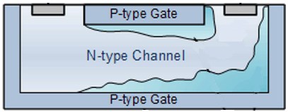
The thickness of this sheet varies according to the degree at the intersection of the reverse bias. In other words, the depletion layer only extends a small way into the channel when there is a small reverse bias and there is a large area to conduct current.
As the gate is positioned with a strong negative bias, the depletion layer rises, spreading deeper into the channel, limiting the region in which current can be performed.
The depletion layer will gradually increase to the degree that it spreads through the channel with increasing bias, and the channel is said to be cut off.
When a current flows through the channel the situation becomes somewhat different. With no gate voltage electrons in the channel, the positive potential on the drain will attract and migrate into it causing a current to pass within the device, and therefore within the external circuit.
The current magnitude depended on a variety of variables which included the channel's cross-sectional field, its length, and conductivity and the voltage applied.
It can be seen from this that the channel serves as a resistor, and a decrease in voltage can occur over its length. As a consequence, it means that as the drain reaches the p-n junction gets increasingly more reverse biased. As a consequence, the depletion layer is denser close to the drain as seen.
As the reverse bias on the gate rises a stage is reached at which the depletion layer almost cuts the channel off. Yet the channel never closes completely. The explanation for this is that the electrostatic forces between the electrons cause them to stretch out, allowing the depletion layer a counter-effect to the thickness rise.
The field around the electrons which flow in the channel successfully opposes any further increase in the depletion layer after a certain level. The voltage at which the depletion layer peaks is called pinch-off voltage.
Ⅲ Parameters of JFET
BVDGO - Drain-to-gate breakdown voltage, with open source. This voltage must not be increased by a cumulative rating or the device will be permanently impaired (unless power dissipation is limited to a reasonable level).
BVGSS - Gate-to-source breakdown voltage, with drain shortening to the source. Only a cumulative value that can not be reached or that will result in irreversible damage (unless power dissipation is kept to a reasonable level).
PD - Minimum Power Dissipation at 25°C ( 77°F) ambient temperature. The need to surpass this absolute limit level or the system will be lost.
IDSS - Drain-to-source current, with gate, shorted to the source (zero gate voltage). Often called pinchoff, or saturation current. This rating shows the highest usable current that can pass through a resistor for output loads. Overcoming the highest IDSS rating triggers the device's landslide, resulting in irreversible damage (unless power dissipation is kept to a safe level).
Yfs - Small-signal, common-source, forward (sometimes called gfs-transconductance) transmittance at 1 kHz. It is the primary competitive value statistic for FET's, as it shows how much gain is available.
VP or VGS(OFF) - Gate-to-source pinchoff (or cutoff) voltage. The gate bias voltage value the reduces drain-to - source current to a very low amount (usually much higher than the value of the lass leakage-current).
Giss - Input (gate-to-source or common-source) capacitance at 1 MHz. This ranking is especially important in rf and switching applications. (Also called Cgss and measured with drain shortened to source.)
IGSS - reverse-bias gate-to-source leakage current, shortened to source by drain. This current of leakage, which is typically low (due to the reverse gate junction), defines impedance of entry, which is usually high (several hundred megohms).
Ⅳ Structure & Fabrication of JFET
JFETs can either be P-channel N-channels. They can be made in very similar ways, with the main exception being that they interchange the N and P areas in the structure below.

Structure of JFET
The N-Channel JFET consists of P-type material in N-type substratum whereas the p-type substratum uses N-type materials to form a P channel JFET.
The JFET is constructed using the long semi-conductor material channel. Based on the design process, if the JFET has a large number of positive charging carriers (referred to as holes), it is a JFET type P, and if it has a large number of negative charging carriers (referred to as electrons) it is called N-type JFET.
Ohmic contacts are created at each end within the long channel of semiconductor materials to form the Source and Drain connections. A P-N junction is formed on one side of the channel or on both.
The devices are often made within a larger substratum and the FET itself is manufactured as shown in the diagram below.
There are a variety of methods to make the FETs. A highly doped substrate usually serves as a second gate for silicon devices.
The active n-type area can then be cultivated using epitaxy, or it can be produced by spreading the impurities into the substrate or by implanting ions.
Where gallium arsenide is used the substratum is formed from an inherent semi-insulating layer. This reduces the levels of any stray capacitances and allows to obtain good high-frequency performance.
The distance between drain and source is significant and should be held to a minimum, regardless of the material used for the FET. It reduces transit times when high-frequency output is needed and provides a low resistance that is critical for power or switching applications while the system is to be used.
JFETs are available in a number of bundles, despite their popularity. They are commonly available on the famous TO92 plastic package as lead electronic parts, as well as many others. Thereafter they are available as surface mount devices in packages including SOT-23 and SOT-223. JFETs are typically used most as surface mount devices. Most large-scale development is carried out using surface mount technology and the mounting systems on the corresponding surface.
While the JFET is less common than the MOSFET with fewer JFETs, it is still a part of great utility. Offering high input impedance, clear bias, low noise, and low cost, it provides a high output quality that can be found in many circumstances.
Related Article:
 UTMEL
UTMEL
We are the professional distributor of electronic components, providing a large variety of products to save you a lot of time, effort, and cost with our efficient self-customized service. careful order preparation fast delivery service
What is JFET and its working?
A JFET is a three terminal semiconductor device in which current conduction is by one type of carrier i.e. electrons or holes. The current conduction is controlled by means of an electric field between the gate and the conducting channel of the device. The JFET has high input impedance and low noise level
Where is JFET used?
The JFET transistors are used as electronically controlled switches, Voltage controlled resistors and as amplifiers. BJT transistors are constructed with the PN-junctions but the JFET transistors have a channel instead of the PN-junctions.
What are the characteristics of JFET?
Fast switching. For low frequency operation, source and drain can be interchanged. Gate voltage that controls drain current. Single majority carrier. Small in size. High “Z” input.
Is JFET and FET same?
FET stands for "Field Effect Transistor" it is a three terminal uni polar solid state device in which current is control by an electric field. P-Channel JFET is similarly is constructed except that it use P- type of bar and two N- types of junctions.
What are the advantages of JFET?
The JFET has high input impedance. The JFET can be fabricated in small size area. It is a majority charge carrier device, hence it has less noise. It is a low power consumption device. It can be fabricated in small size area. It occupies less space in circuits due to its smaller size.
 MOSFET vs. IGBT: Characteristics, Structure and Market AnalysisUTMEL25 December 202523111
With the rise of new energy in recent years, the market demand for MOSFETs and IGBTs is increasing steeply. Generally used as switching devices, they are widely used in electronic circuits. MOSFETs and IGBTs are relatively similar in appearance and characteristics parameters. So what is the difference between MOSFETs and IGBTs?
Read More Introduction to FinFETUTMEL18 March 202130067
The full name of FinFET is Fin Field-Effect Transistor. It is a new complementary metal oxide semiconductor transistor. The FinFET name is based on the similarity between the shape of the transistor and the fin.
Read More What is a MOSFET?UTMEL16 April 20217337
MOSFET, short for Metal-Oxide-Semiconductor Field-Effect Transistor, is a field-effect transistor that can be widely used in analog circuits and digital circuits. MOSFETs can be divided into N-channel type with the majority of electrons and P-channel type with the majority of holes according to their "channel" polarity. They are usually called NMOSFET and PMOSFET.
Read More NPN Transistors and PNP TransistorsUTMEL29 October 20209674
NPN and PNP are two types of transistors. Transistors are semiconductor devices made of doped p-type and n-type junctions. This article mainly introduces the differences between this two kinds of transistors, the methods of distinguishing them, and the application of them.
Read More An Overview of Bipolar TransistorsUTMEL27 August 20208947
Bipolar Transistor, full name bipolar junction transistor(BJT), is an electronic device with three terminals, made of three parts of semiconductors with different levels of doping. The charge flow in the transistor is mainly due to the diffusion and drift movement of carriers at the PN junction.
Read More
Subscribe to Utmel !
![BLM15AG102SN1D]() BLM15AG102SN1D
BLM15AG102SN1DMurata Electronics
![CMP04FSZ]() CMP04FSZ
CMP04FSZAnalog Devices Inc.
![7BB-35-3]() 7BB-35-3
7BB-35-3Murata Electronics
![PKM22EPPH2001-B0]() PKM22EPPH2001-B0
PKM22EPPH2001-B0Murata Electronics
![GRM155R60J475ME87D]() GRM155R60J475ME87D
GRM155R60J475ME87DMurata Electronics
![BLM18PG330SN1D]() BLM18PG330SN1D
BLM18PG330SN1DMurata Electronics
![ENW-89847A3KF]() ENW-89847A3KF
ENW-89847A3KFPanasonic Electronic Components
![GCM1885C2A150JA16D]() GCM1885C2A150JA16D
GCM1885C2A150JA16DMurata Electronics
![AVRL101A3R3FTA]() AVRL101A3R3FTA
AVRL101A3R3FTATDK Corporation
![BLM03AX102SN1D]() BLM03AX102SN1D
BLM03AX102SN1DMurata Electronics


