Apple M1 Ultra -- The Technology Behind the Chip Interconnection

M1 Ultra — How Apple DESTROYED Nvidia

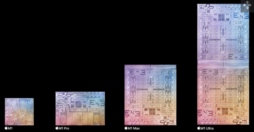
Nowadays, manufacturing high-performance microprocessors are becoming increasingly tricky and expensive. That's why developers must choose complex packaging technologies and designs for performance-demanding applications. Apple acknowledges that it had to fuse two M1 Max system chips together to build the M1 Ultra processor. But it did not say it had to use one of TSMC's most advanced packaging technologies to build the M1 Ultra.
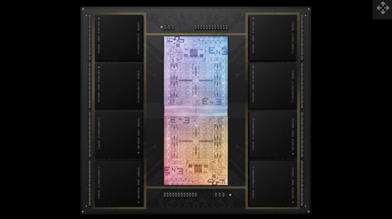
Fortunately, unofficial sources are not as secretive as Apple and were able to dig up more details about the interconnect between Apple's UltraFusion processors. The processor offers 2.5 TB/s of bandwidth. Media reports indicate that Apple's M1 Ultra processors are built using TSMC's CoWoS-S (wafer-on-chip substrate with silicon interposer) 2.5D interposer-based packaging process for the M1 Ultra. AMD, Nvidia, and Fujitsu are among the companies using similar technology to build high-performance processors for data centers and high-performance computing (HPC).
There is no doubt that Apple's M1 Ultra is a powerful design. Each M1 Max SoC has a die size of 432mm². So the M1Ultra must use more than 860mm² of intermediate layers. AMD and Nvidia use larger intermediate layers and their compute GPUs have high bandwidth memory.
But TSMC's CoWoS-S is not the world's largest semiconductor manufacturer's only option for bandwidth-intensive applications. Some experts speculate that Apple may choose TSMC's InFO_LSI technology for ultra-high-bandwidth small-chip integration. Unlike CoWoS-S, InFO_LSI uses local silicon interconnects rather than large and expensive intermediary layers. Intel's Embedded Chip Interconnect Bridge (EMIB) uses the same concept.
Apple showed an M1 Max die shot with a large I/O pad, similar to a native interconnect designed to connect to an intermediate chip. Therefore, it is not surprising that many believe Apple uses InFO_LSI.
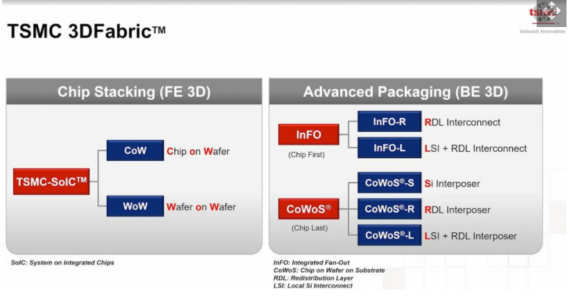
But there may be a reason why Apple is sticking with the more expensive CoWoS-S. TSMC's InFO_LSI officially launches in August 2020 and is scheduled to be certified by Q1 2021. Meanwhile, Apple's M1 Max will enter mass production in Q2 or Q3 of 2021. So Apple may simply not have enough time to implement InFO_LSI, or it may decide not to take any chances and stick with well-known technologies that are widely used by various companies.
DigiTimes revealed that Unimicron Technology is currently Apple's only ABF substrate supplier, as it is the only company that can provide the quality and quantity Apple needs. In any case, while we now know what packaging technology Apple is using to implement UltraFusion interconnect, we still don't know its clocking, bus width, power, etc.
Related News
1、MediaTek, Qualcomm announce joining Russia sanctions
2、Automotive chips rose across the board!
3、Apple M1 Ultra -- The Technology Behind the Chip Interconnection
4、Foxconn Announces Investment of $9 Billion to Build A Chip Factory in Saudi Arabia
5、Japanese Companies Increase Investment in Power Semiconductors
 UTMEL 2024 Annual gala: Igniting Passion, Renewing BrillianceUTMEL18 January 20244830
As the year comes to an end and the warm sun rises, Utmel Electronics celebrates its 6th anniversary.
Read More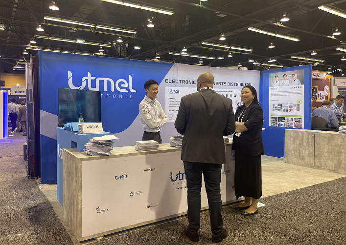 Electronic Components Distributor Utmel to Showcase at 2024 IPC APEX EXPOUTMEL10 April 20245818
Utmel, a leading electronic components distributor, is set to make its appearance at the 2024 IPC APEX EXPO.
Read More Electronic components distributor UTMEL to Showcase at electronica ChinaUTMEL07 June 20244401
The three-day 2024 Electronica China will be held at the Shanghai New International Expo Center from July 8th to 10th, 2024.
Read More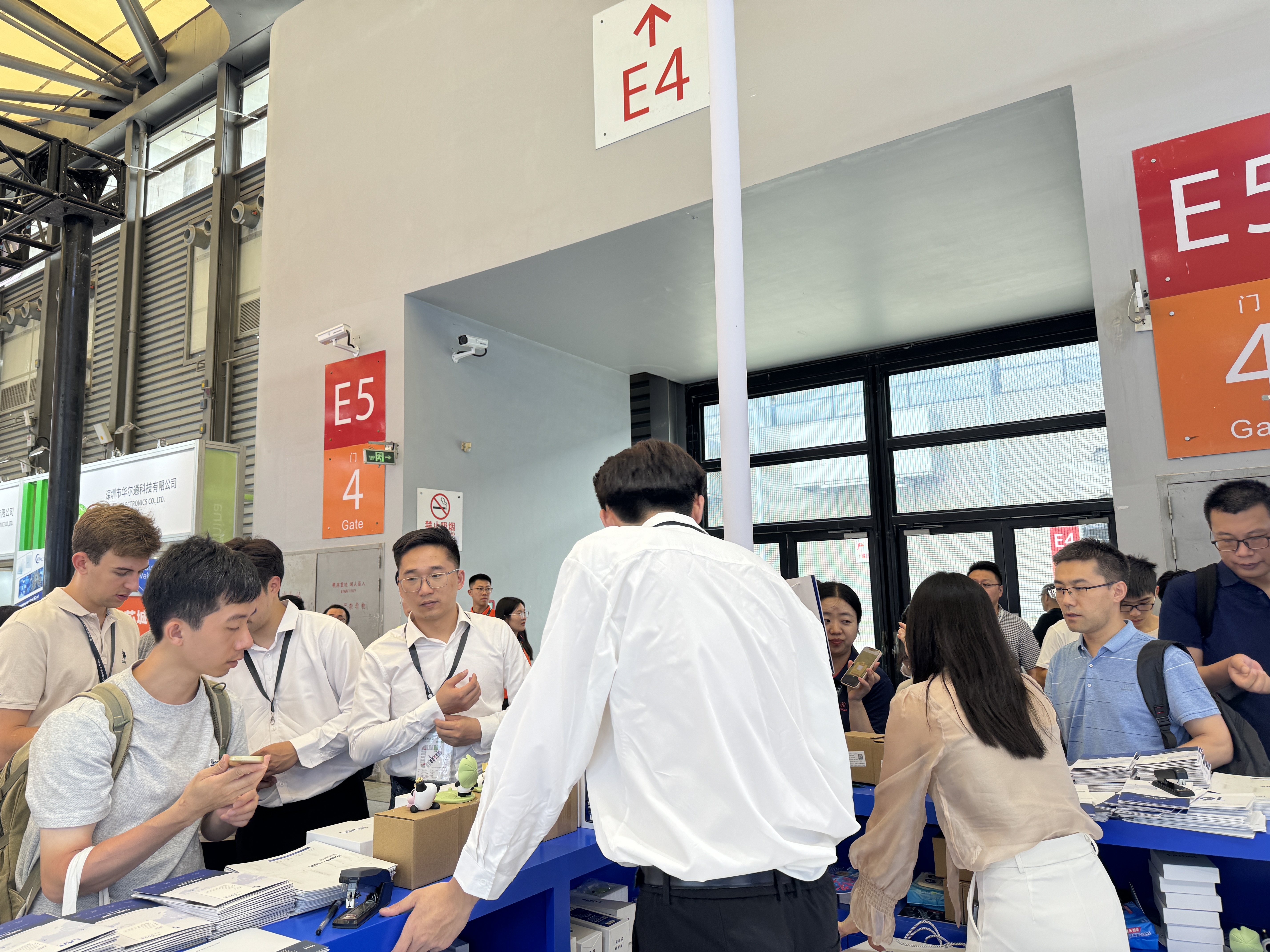 Electronic components distributor UTMEL Stands Out at electronica china 2024UTMEL09 July 20244770
From July 8th to 10th, the three-day electronica china 2024 kicked off grandly at the Shanghai New International Expo Center.
Read More A Combo for Innovation: Open Source and CrowdfundingUTMEL15 November 20195353
Open source is already known as a force multiplier, a factor that makes a company's staff, financing, and resources more effective. However, in the last few years, open source has started pairing with another force multiplier—crowdfunding. Now the results of this combination are starting to emerge: the creation of small, innovative companies run by design engineers turned entrepreneurs. Although the results are just starting to appear, they include a fresh burst of product innovation and further expansion of open source into business.
Read More
Subscribe to Utmel !
![PT10LH01-501A2020-PM-S]() PT10LH01-501A2020-PM-S
PT10LH01-501A2020-PM-SAmphenol Piher Sensing Systems
![AME15-24SMAZ-E]() AME15-24SMAZ-E
AME15-24SMAZ-Eaimtec
![AMEOF3-24SLJZ-450]() AMEOF3-24SLJZ-450
AMEOF3-24SLJZ-450aimtec
![AMEOF3-12SBJZ-324]() AMEOF3-12SBJZ-324
AMEOF3-12SBJZ-324aimtec
![AMEOF1-9SJZ-120]() AMEOF1-9SJZ-120
AMEOF1-9SJZ-120aimtec
![PT10LH01-205A2020]() PT10LH01-205A2020
PT10LH01-205A2020Amphenol Piher Sensing Systems
![PT10LH01-221A2020-PM-S]() PT10LH01-221A2020-PM-S
PT10LH01-221A2020-PM-SAmphenol Piher Sensing Systems
![PT15NV02-101A2020-S]() PT15NV02-101A2020-S
PT15NV02-101A2020-SAmphenol Piher Sensing Systems
![PT10LV10-303A2020]() PT10LV10-303A2020
PT10LV10-303A2020Amphenol Piher Sensing Systems
![PT10LH01-303A2020]() PT10LH01-303A2020
PT10LH01-303A2020Amphenol Piher Sensing Systems


 Product
 Brand
Brand Articles
 Tools
Tools


