Product
 Brand
Brand Articles
 Tools
Tools
The Art of Microchips: A Journey from Sand to Silicon
Microchips, the tiny semiconductors that power our world, have a near-divine creation story. At the heart of this story is silicon, the second-most common element on Earth, considered by many in the industry as a gift from God. The process of making microchips starts with silica sand, a material found in abundance on our planet. This sand is heated, spun, and then a small seed crystal is dipped into the hot mixture to create a large single-crystal silicon ingot. This ingot is then sliced into flat wafers, which are polished to remove all blemishes, creating the flattest objects in the world. The real magic happens when these wafers are processed into chips. Using photolithography machines, atomic-sized transistors are carved, layered, and latticed onto the wafer, creating a semiconductive nano-universe. The process of etching on materials a few atoms thick is a kind of transubstantiation, turning sand into mind. Each chip, with billions or even trillions of transistors and wires stacked on it, amounts to an atomic multidimensional chessboard. The potential combinations of ons and offs can only be considered endless. However, the history of the microchip is not without controversy. The transistors on the microchip were the brainchild of a eugenicist, William Shockley. Despite his problematic legacy, the microchip industry has evolved to become a cornerstone of modern technology, with companies like Taiwan Semiconductor Manufacturing Co. (TSMC) leading the way. TSMC, which makes 92 percent of the world’s most avant-garde chips, is at the forefront of this atomic construction, pushing the boundaries of what is possible in the realm of microchip technology.
 UTMEL
UTMEL
We are the professional distributor of electronic components, providing a large variety of products to save you a lot of time, effort, and cost with our efficient self-customized service. careful order preparation fast delivery service
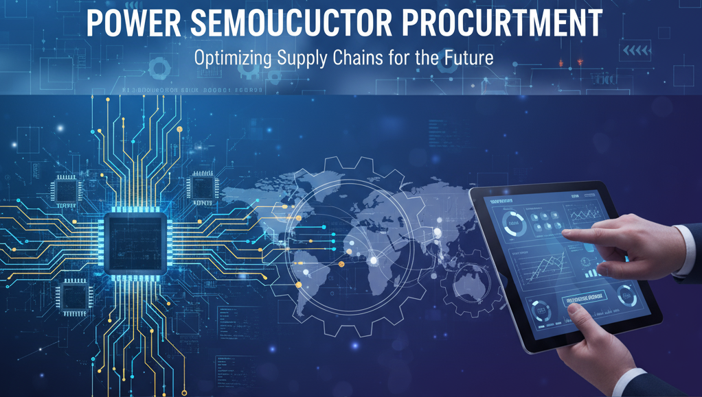 Power Semiconductor Procurement After the Nexperia Shake-Up—NXP for Stability, ON for Technology, or Nexperia for Value?UTMEL04 November 20254806
The recent supply chain turmoil surrounding Netherlands-based Nexperia has sent shockwaves through the global semiconductor industry, forcing procurement professionals to re-evaluate their sourcing strategies.
Read More AI Computing Power Gap: How Token Consumption is Reshaping Server Component SourcingUTMEL23 June 2026889
As global token consumption drives the transition to high-density 100kW+ AI data centers, power delivery networks require advanced Wide-Bandgap semiconductors (SiC/GaN) and high-capacitance MLCCs. This shift has triggered a component procurement crisis with lead times exceeding 24 weeks. To bypass shortages, hardware buyers must abandon just-in-time manufacturing and leverage independent global distributor networks to secure critical power and passive components.
Read More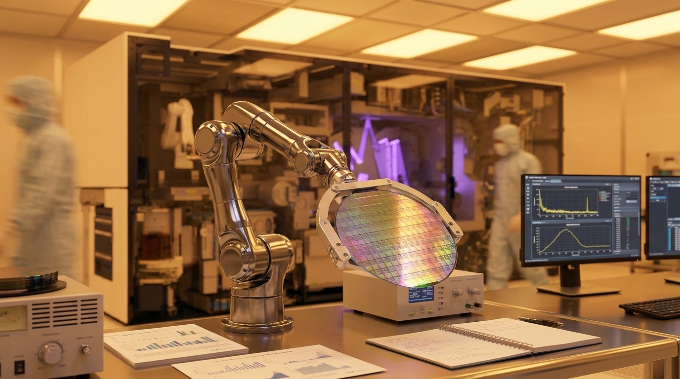 The BSPDN Revolution: Overcoming IR Drop in Sub-2nm GAAFET Nodes with Backside Power DeliveryUTMEL25 June 2026788
As semiconductor manufacturing enters the sub-2nm era, Backside Power Delivery Networks (BSPDN) are replacing traditional front-side routing to overcome critical IR drop bottlenecks. By separating power and signal delivery, chipmakers like Intel and TSMC drastically improve performance and density in GAAFET designs. However, this radical shift introduces manufacturing complexities, thermal challenges, and demands advanced packaging and power management solutions.
Read More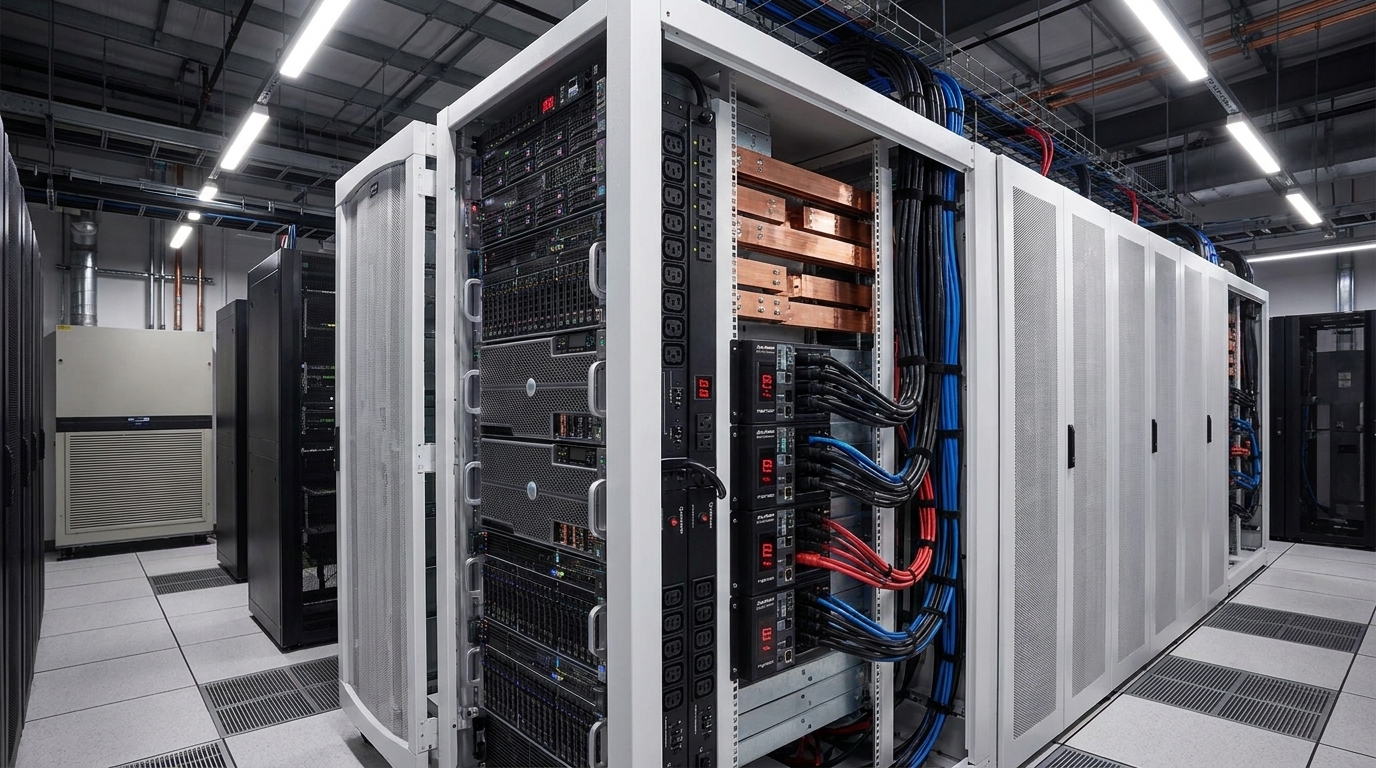 Power Management ICs Trends 2026: AI Demand, Supply Risks, and Sourcing StrategiesUTMEL06 July 20261261
As AI server racks surpass 100kW by 2026, data centers are shifting toward wide-bandgap semiconductors like SiC and GaN. However, this demand has triggered a critical shortage of mature-node Power Management ICs (PMICs). To prevent production halts, sourcing teams must abandon 'just-in-time' models, implement proactive 'just-in-case' strategies, and rapidly qualify pin-to-pin alternative components to secure their supply chains.
Read More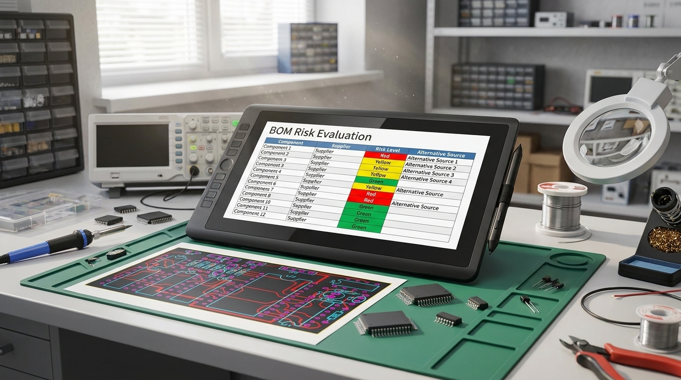 onsemi Synaptics Acquisition Impact: BOM Risk Checklist and Second-Source Strategy for Edge AI DesignsUTMEL27 July 2026287
The onsemi acquisition of Synaptics provides hardware program managers a 12-to-18-month window before potential product cancellations occur in mid-2027. This guide outlines how to audit BOM exposure across overlap and non-core product lines, calculate Last-Time-Buy volumes including hidden storage costs, establish proactive second-sourcing triggers, and implement supply chain monitoring to prevent line-down events.
Read More
Subscribe to Utmel !
![BLM15AX601SN1D]() BLM15AX601SN1D
BLM15AX601SN1DMurata Electronics
![BLM18HD102SN1D]() BLM18HD102SN1D
BLM18HD102SN1DMurata Electronics
![H050X044H1T]() H050X044H1T
H050X044H1TPanduit Corp
![SNR-10-223]() SNR-10-223
SNR-10-223Cosel USA, Inc.
![1-22279-6]() 1-22279-6
1-22279-6TE Application Tooling
![H100X044H1T-2]() H100X044H1T-2
H100X044H1T-2Panduit Corp
![83500000005]() 83500000005
83500000005Littelfuse Inc.
![BLM18SG700TN1D]() BLM18SG700TN1D
BLM18SG700TN1DMurata Electronics
![EMPLUS-2GO]() EMPLUS-2GO
EMPLUS-2GOPanduit Corp
![56000001009]() 56000001009
56000001009Littelfuse Inc.