74HC00 Quadruple 2-Input NAND Gates: 74LS Series vs. 74HC Series
15 ns ns 135 ns ns 8.74mm mm Gates & Inverters 1.48mm mm Surface Mount Surface Mount 2V~6V V 20μA μA
Unit Price: $0.217765
Ext Price: $0.22


15 ns ns 135 ns ns 8.74mm mm Gates & Inverters 1.48mm mm Surface Mount Surface Mount 2V~6V V 20μA μA
The 74HC00 provides four independent 2-input NAND gates with standard push-pull outputs. Furthermore, Huge range of Semiconductors, Capacitors, Resistors and IcS in stock. Welcome RFQ.

Quick 7400 74HC00 Quad 2 input NAND logic gate integrated circuit IC demonstration by electronzap
- 74HC00 Pinout
- 74HC00 CAD Model
- 74HC00 Overview
- 74HC00 Features
- Specifications
- 74HC00 Functional Block Diagram
- 74HC00 Parameter Measurement Information
- 74HC00 Equivalent
- Parts with Similar Specs
- When to use 74HC series chips?
- 74LS Series vs. 74HC Series
- 74HC00 Application
- 74HC00 Package
- 74HC00 Marking Information
- 74HC00 Suggested Pad Layout
- 74HC00 Manufacturer
- Datasheet PDF
- Trend Analysis
74HC00 Pinout

Pinout
| Pin Number | Pin Name | Function |
| 1 | 1A | Data Input |
| 2 | 1B | Data Input |
| 3 | 1Y | Data Output |
| 4 | 2A | Data Input |
| 5 | 2B | Data Input |
| 6 | 2Y | Data Output |
| 7 | GND | Ground |
| 8 | 3Y | Data Output |
| 9 | 3A | Data Input |
| 10 | 3B | Data Input |
| 11 | 4Y | Data Output |
| 12 | 4A | Data Input |
| 13 | 4B | Data Input |
| 14 | VCC | Supply Voltage |
Pin description
74HC00 CAD Model
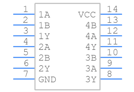
Symbol
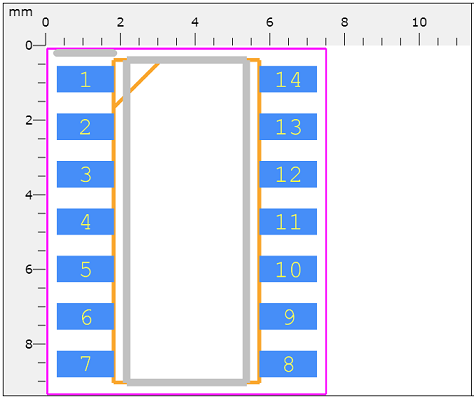
Footprint
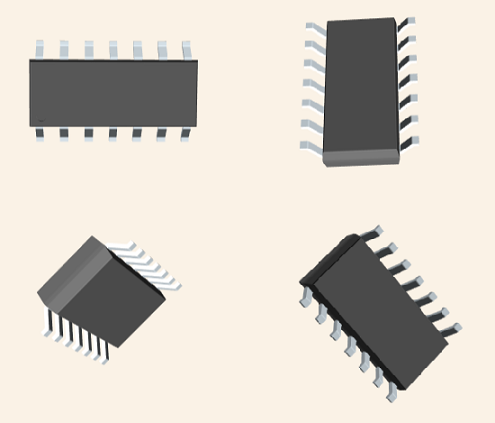
3D Model
74HC00 Overview
The 74HC00 provides four independent 2-input NAND gates with standard push-pull outputs. The device is designed for operation with a power supply range of 2.0V to 6.0V.
This article provides you with a basic overview of the 74HC00, including its pin descriptions, features and specifications, etc., to help you quickly understand what 74HC00 is.
74HC00 Features
● Wide Supply Voltage Range from 2.0V to 6.0V
● Sinks or Sources 4mA at VCC = 4.5V
● CMOS Low Power Consumption
● Schmitt Trigger Action at All Inputs
● ESD Protection Exceeds JESD 22
◆ 200-V Machine Model (A115-A)
◆ 2000-V Human Body Model (A114-A)
◆ Exceeds 1000-V Charged Device Model (C101C)
● Range of Package Options SO-14 and TSSOP-14
● Totally Lead-Free & Fully RoHS Compliant
● Halogen and Antimony Free. “Green” Device
Specifications
- TypeParameter
- Mount
In electronic components, the term "Mount" typically refers to the method or process of physically attaching or fixing a component onto a circuit board or other electronic device. This can involve soldering, adhesive bonding, or other techniques to secure the component in place. The mounting process is crucial for ensuring proper electrical connections and mechanical stability within the electronic system. Different components may have specific mounting requirements based on their size, shape, and function, and manufacturers provide guidelines for proper mounting procedures to ensure optimal performance and reliability of the electronic device.
Surface Mount - Mounting Type
The "Mounting Type" in electronic components refers to the method used to attach or connect a component to a circuit board or other substrate, such as through-hole, surface-mount, or panel mount.
Surface Mount - Package / Case
refers to the protective housing that encases an electronic component, providing mechanical support, electrical connections, and thermal management.
14-SOIC (0.154, 3.90mm Width) - Number of Pins14
- Logic Level-High1.5V ~ 4.2V
- Logic Level-Low0.5V ~ 1.8V
- Operating Temperature
The operating temperature is the range of ambient temperature within which a power supply, or any other electrical equipment, operate in. This ranges from a minimum operating temperature, to a peak or maximum operating temperature, outside which, the power supply may fail.
-40°C~125°C TA - Packaging
Semiconductor package is a carrier / shell used to contain and cover one or more semiconductor components or integrated circuits. The material of the shell can be metal, plastic, glass or ceramic.
Tape & Reel (TR) - Series
In electronic components, the "Series" refers to a group of products that share similar characteristics, designs, or functionalities, often produced by the same manufacturer. These components within a series typically have common specifications but may vary in terms of voltage, power, or packaging to meet different application needs. The series name helps identify and differentiate between various product lines within a manufacturer's catalog.
74HC - Published2013
- JESD-609 Code
The "JESD-609 Code" in electronic components refers to a standardized marking code that indicates the lead-free solder composition and finish of electronic components for compliance with environmental regulations.
e3 - Pbfree Code
The "Pbfree Code" parameter in electronic components refers to the code or marking used to indicate that the component is lead-free. Lead (Pb) is a toxic substance that has been widely used in electronic components for many years, but due to environmental concerns, there has been a shift towards lead-free alternatives. The Pbfree Code helps manufacturers and users easily identify components that do not contain lead, ensuring compliance with regulations and promoting environmentally friendly practices. It is important to pay attention to the Pbfree Code when selecting electronic components to ensure they meet the necessary requirements for lead-free applications.
yes - Part Status
Parts can have many statuses as they progress through the configuration, analysis, review, and approval stages.
Active - Moisture Sensitivity Level (MSL)
Moisture Sensitivity Level (MSL) is a standardized rating that indicates the susceptibility of electronic components, particularly semiconductors, to moisture-induced damage during storage and the soldering process, defining the allowable exposure time to ambient conditions before they require special handling or baking to prevent failures
1 (Unlimited) - Number of Terminations14
- Terminal Finish
Terminal Finish refers to the surface treatment applied to the terminals or leads of electronic components to enhance their performance and longevity. It can improve solderability, corrosion resistance, and overall reliability of the connection in electronic assemblies. Common finishes include nickel, gold, and tin, each possessing distinct properties suitable for various applications. The choice of terminal finish can significantly impact the durability and effectiveness of electronic devices.
Matte Tin (Sn) - Voltage - Supply
Voltage - Supply refers to the range of voltage levels that an electronic component or circuit is designed to operate with. It indicates the minimum and maximum supply voltage that can be applied for the device to function properly. Providing supply voltages outside this range can lead to malfunction, damage, or reduced performance. This parameter is critical for ensuring compatibility between different components in a circuit.
2V~6V - Terminal Position
In electronic components, the term "Terminal Position" refers to the physical location of the connection points on the component where external electrical connections can be made. These connection points, known as terminals, are typically used to attach wires, leads, or other components to the main body of the electronic component. The terminal position is important for ensuring proper connectivity and functionality of the component within a circuit. It is often specified in technical datasheets or component specifications to help designers and engineers understand how to properly integrate the component into their circuit designs.
DUAL - Terminal Form
Occurring at or forming the end of a series, succession, or the like; closing; concluding.
GULL WING - Peak Reflow Temperature (Cel)
Peak Reflow Temperature (Cel) is a parameter that specifies the maximum temperature at which an electronic component can be exposed during the reflow soldering process. Reflow soldering is a common method used to attach electronic components to a circuit board. The Peak Reflow Temperature is crucial because it ensures that the component is not damaged or degraded during the soldering process. Exceeding the specified Peak Reflow Temperature can lead to issues such as component failure, reduced performance, or even permanent damage to the component. It is important for manufacturers and assemblers to adhere to the recommended Peak Reflow Temperature to ensure the reliability and functionality of the electronic components.
260 - Number of Functions4
- Supply Voltage
Supply voltage refers to the electrical potential difference provided to an electronic component or circuit. It is crucial for the proper operation of devices, as it powers their functions and determines performance characteristics. The supply voltage must be within specified limits to ensure reliability and prevent damage to components. Different electronic devices have specific supply voltage requirements, which can vary widely depending on their design and intended application.
4.5V - Time@Peak Reflow Temperature-Max (s)
Time@Peak Reflow Temperature-Max (s) refers to the maximum duration that an electronic component can be exposed to the peak reflow temperature during the soldering process, which is crucial for ensuring reliable solder joint formation without damaging the component.
40 - Pin Count
a count of all of the component leads (or pins)
14 - Supply Voltage-Max (Vsup)
The parameter "Supply Voltage-Max (Vsup)" in electronic components refers to the maximum voltage that can be safely applied to the component without causing damage. It is an important specification to consider when designing or using electronic circuits to ensure the component operates within its safe operating limits. Exceeding the maximum supply voltage can lead to overheating, component failure, or even permanent damage. It is crucial to adhere to the specified maximum supply voltage to ensure the reliable and safe operation of the electronic component.
6V - Supply Voltage-Min (Vsup)
The parameter "Supply Voltage-Min (Vsup)" in electronic components refers to the minimum voltage level required for the component to operate within its specified performance range. This parameter indicates the lowest voltage that can be safely applied to the component without risking damage or malfunction. It is crucial to ensure that the supply voltage provided to the component meets or exceeds this minimum value to ensure proper functionality and reliability. Failure to adhere to the specified minimum supply voltage may result in erratic behavior, reduced performance, or even permanent damage to the component.
2V - Number of Circuits4
- Propagation Delay
the flight time of packets over the transmission link and is limited by the speed of light.
15 ns - Quiescent Current
The quiescent current is defined as the current level in the amplifier when it is producing an output of zero.
20μA - Turn On Delay Time
Turn-on delay, td(on), is the time taken to charge the input capacitance of the device before drain current conduction can start.
135 ns - Family
In electronic components, the parameter "Family" typically refers to a categorization or classification system used to group similar components together based on their characteristics, functions, or applications. This classification helps users easily identify and select components that meet their specific requirements. The "Family" parameter can include various subcategories such as resistors, capacitors, diodes, transistors, integrated circuits, and more. Understanding the "Family" of an electronic component can provide valuable information about its compatibility, performance specifications, and potential uses within a circuit or system. It is important to consider the "Family" parameter when designing or troubleshooting electronic circuits to ensure proper functionality and compatibility with other components.
HC/UH - Logic Function
In electronic components, the term "Logic Function" refers to the specific operation or behavior of a component based on its input signals. It describes how the component processes the input signals to produce the desired output. Logic functions are fundamental to digital circuits and are used to perform logical operations such as AND, OR, NOT, and XOR.Each electronic component, such as logic gates or flip-flops, is designed to perform a specific logic function based on its internal circuitry. By understanding the logic function of a component, engineers can design and analyze complex digital systems to ensure proper functionality and performance. Different logic functions can be combined to create more complex operations, allowing for the creation of sophisticated digital devices and systems.
NAND - Number of Inputs2
- Logic Type
Logic Type in electronic components refers to the classification of circuits based on the logical operations they perform. It includes types such as AND, OR, NOT, NAND, NOR, XOR, and XNOR, each defining the relationship between binary inputs and outputs. The logic type determines how the inputs affect the output state based on specific rules of Boolean algebra. This classification is crucial for designing digital circuits and systems, enabling engineers to select appropriate components for desired functionalities.
NAND Gate - Max Propagation Delay @ V, Max CL
The parameter "Max Propagation Delay @ V, Max CL" in electronic components refers to the maximum amount of time it takes for a signal to propagate through the component from input to output when operating at a specific voltage (V) and driving a maximum specified load capacitance (CL). This parameter is crucial in determining the speed and performance of the component in a circuit. A shorter propagation delay indicates faster signal processing and better overall performance. Designers use this parameter to ensure that signals can be transmitted and received within the required timing constraints in their electronic systems.
15ns @ 6V, 50pF - Schmitt Trigger Input
The Schmitt Trigger is a logic input type that provides hysteresis or two different threshold voltage levels for rising and falling edge.
Yes - Height1.48mm
- Length8.74mm
- Width3.99mm
- REACH SVHC
The parameter "REACH SVHC" in electronic components refers to the compliance with the Registration, Evaluation, Authorization, and Restriction of Chemicals (REACH) regulation regarding Substances of Very High Concern (SVHC). SVHCs are substances that may have serious effects on human health or the environment, and their use is regulated under REACH to ensure their safe handling and minimize their impact.Manufacturers of electronic components need to declare if their products contain any SVHCs above a certain threshold concentration and provide information on the safe use of these substances. This information allows customers to make informed decisions about the potential risks associated with using the components and take appropriate measures to mitigate any hazards.Ensuring compliance with REACH SVHC requirements is essential for electronics manufacturers to meet regulatory standards, protect human health and the environment, and maintain transparency in their supply chain. It also demonstrates a commitment to sustainability and responsible manufacturing practices in the electronics industry.
No SVHC - Radiation Hardening
Radiation hardening is the process of making electronic components and circuits resistant to damage or malfunction caused by high levels of ionizing radiation, especially for environments in outer space (especially beyond the low Earth orbit), around nuclear reactors and particle accelerators, or during nuclear accidents or nuclear warfare.
No - RoHS Status
RoHS means “Restriction of Certain Hazardous Substances” in the “Hazardous Substances Directive” in electrical and electronic equipment.
ROHS3 Compliant - Lead Free
Lead Free is a term used to describe electronic components that do not contain lead as part of their composition. Lead is a toxic material that can have harmful effects on human health and the environment, so the electronics industry has been moving towards lead-free components to reduce these risks. Lead-free components are typically made using alternative materials such as silver, copper, and tin. Manufacturers must comply with regulations such as the Restriction of Hazardous Substances (RoHS) directive to ensure that their products are lead-free and environmentally friendly.
Lead Free
74HC00 Functional Block Diagram

Logic Diagram
74HC00 Parameter Measurement Information
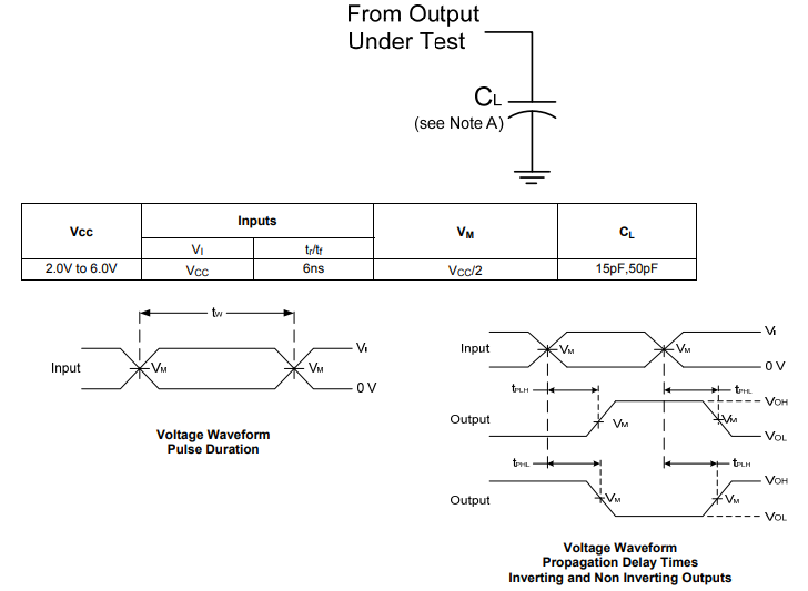
Load Circuit and Voltage Waveforms
74HC00 Equivalent
| Model number | Manufacturer | Description |
| 74HC03DB,118 | NXP Semiconductors | 74HC(T)03 - Quad 2-input NAND gate SSOP1 14-Pin |
| M54HC00F1 | SGS-Ates Componenti Electronici SPA | NAND Gate, CMOS, CDIP14 |
| CD74HC00MTE4 | Rochester Electronics LLC | NAND Gate, HC/UH Series, 4-Func, 2-Input, CMOS, PDSO14, GREEN, PLASTIC, MS-012AB, SOIC-14 |
| 74HCT132D | Philips Semiconductors | NAND Gate, CMOS, PDSO14 |
| 74HC00DB-T | NXP Semiconductors | IC HC/UH SERIES, QUAD 2-INPUT NAND GATE, PDSO14, 5.30 MM, PLASTIC, MO-150, SOT337-1, SSOP-14, Gate |
| M74HC00M1 | STMicroelectronics | HC/UH SERIES, QUAD 2-INPUT NAND GATE, PDSO14, MICRO, PLASTIC, GULLWING, DIP-14 |
| SN74HCT00DTE4 | Texas Instruments | HCT SERIES, QUAD 2-INPUT NAND GATE, PDSO14, GREEN, PLASTIC, SOIC-14 |
| 74HC00D/T3 | NXP Semiconductors | IC HC/UH SERIES, QUAD 2-INPUT NAND GATE, PDSO14, 3.90 MM, PLASTIC, MS-012, SOT-108-1, SOP-14, Gate |
| MM74HC132M | Rochester Electronics LLC | HC/UH SERIES, QUAD 2-INPUT NAND GATE, PDSO14, 0.150 INCH, MS-012, SOIC-14 |
| MC54HC00AJD | Motorola Semiconductor Products | NAND Gate, HC/UH Series, 4-Func, 2-Input, CMOS, CDIP14, CERAMIC, DIP-14 |
Parts with Similar Specs
- ImagePart NumberManufacturerPackage / CaseNumber of InputsNumber of PinsLogic FunctionNumber of CircuitsPropagation DelaySupply VoltageQuiescent CurrentView Compare
74HC00S14-13
14-SOIC (0.154, 3.90mm Width)
2
14
NAND
4
15 ns
4.5 V
20 μA
14-SOIC (0.154, 3.90mm Width)
2
14
NAND
4
4.1 ns
3.3 V
40 μA
14-SOIC (0.154, 3.90mm Width)
2
14
NAND, Schmitt Trigger
-
21 ns
5 V
2 μA
14-SOIC (0.154, 3.90mm Width)
2
14
AND, NAND
-
7 ns
5 V
40 μA
14-SOIC (0.154, 3.90mm Width)
2
14
NAND
-
16 ns
5 V
2 μA
When to use 74HC series chips?
When to use CD40 chip? When to use 74LS series chips? When to use 74HC series chips? Under what circumstances can chips with the same logic function convert each other?
The CMOS chip has a wide power supply voltage and low power consumption, while the 74LS series power supply voltage must be 5V and high power consumption. Therefore, when the power supply voltage is not 5V or the circuit power consumption is required to be low, such as battery power supply, it is required to save Electricity and the voltage is not 5V, it is suitable to use CMOS chip, but its driving ability is relatively small. When a larger drive capability is required, the 74LS chip is appropriate. For example, when power saving is required at the same time, the 74HC chip is appropriate. Now 74HC is almost substituted for the 74LS chip, because it has the advantages of both CMOS and 74LS. As long as the 74HC and 74LS chips are of the same model, the two can be directly replaced.
74LS Series vs. 74HC Series
The difference between 74LS series and 74HC series of electronic circuits is:
1. LS is a low-power Schottky, HC is a high-speed COMS. The speed of LS is slightly faster than that of HC. HCT input and output are compatible with LS, but low power consumption; F is a high-speed Schottky circuit;
2. LS is TTL level, HC is CMOS level.
3. The LS input is open for high level, and the HC input is not allowed to be open. HC generally requires a pull-up and pull- down resistor to determine the level when the input is invalid. LS does not have this requirement
4. The pull-down of LS output is strong and the pull-up is weak. The pull-up and pull-down of HC are the same.
5. The working voltage is different, LS can only use 5V, while HC is generally 2V to 6V;
6. The level is different. LS is TTL level, its low level and high level are 0.8V and 2.4V respectively, while CMOS is 0.3V and 3.6V when the working voltage is 5V, so CMOS can drive TTL, but the reverse is not possible
7. The driving ability is different. The driving ability of LS is generally 5mA for high level and 20mA for low level; while the high and low level of CMOS are both 5mA;
8. CMOS devices have poor antistatic ability and are prone to latching problems, so the input pins of CMOS cannot be directly connected to power.
74HC00 Application
● General Purpose Logic
● Wide array of products such as:
◆ PCs, Networking, Notebooks, Netbooks
◆ Computer Peripherals, Hard Drives, CD/DVD ROM
◆ TV, DVD, DVR, Set Top Box
74HC00 Package
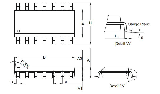
Package
74HC00 Marking Information

Marking Information
74HC00 Suggested Pad Layout
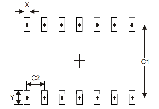
Suggested Pad Layout
74HC00 Manufacturer
Diodes Incorporated (Nasdaq: DIOD), a Standard and Poor's Smallcap 600 and Russell 3000 Index company, is a leading global manufacturer and supplier of high-quality application-specific standard products within the broad discrete, logic, analog, and mixed-signal semiconductor markets. Diodes serves the consumer electronics, computing, communications, industrial, and automotive markets.
Diodes Incorporated is devoted to be the leading provider for large-volume and high-growing markets. With cutting-edge products of package technology, analog, discrete and mixed-signal products, Diodes Incorporated is capable to provide high-quality semiconductor products to meet the customers' needs from walks of communications, computing, consumer electronics, automotive and industrial markets. Their product lines cover a wide range of application solutions together with 25 operations around the world which serve with examine, engineering, manufacturing and customer service.
Datasheet PDF
- Environmental Information :
- RohsStatement :
- Datasheets :
Trend Analysis
Is 74LS00P the same as 74HC00?
Both 74LS00P and 74HC00 are Quadruple 2-Input NAND Gates. 74LS00P is a TTL device with a working power supply voltage of 5V; 74HC00 is a CMOS device with a working power supply voltage of 2V-6V.
Is 74LS00 interchangeable with 74HC00?
74HC00 and 74LS00 are of the same model, 74HC00 is a high-speed circuit, 74LS00 is a low-speed circuit, 74HC00 can replace 74LS00, but not vice versa.
What are the similarities and differences between CD4011, 74LS00, and 74HC00?
CD4011, 74LS00, 74HC00 are all 2-input four-NAND gates. The pin arrangement of CD4011 and 74LS00, 74HC00 is different. 74LS00 and 74HC00 have the same pin arrangement. CD4011 is a CMOS device with a power supply operating voltage of 3V-18V. 74LS00 is a TTL device, and the operating voltage of the power supply is 5V. 74HC00 is a high-speed CMOS device with a power supply voltage of 2V-6V.
![2N3053 BJT Transistor: Datasheet, Pinout, Circuit [FAQ&Video]](https://res.utmel.com/Images/Article/73b60587-50f2-45df-b152-447f4f044b9f.jpg) 2N3053 BJT Transistor: Datasheet, Pinout, Circuit [FAQ&Video]
2N3053 BJT Transistor: Datasheet, Pinout, Circuit [FAQ&Video]04 May 20223486
 IRF830 Power MOSFET: Pinout, Datasheet, and Test Circuit
14 July 20214711
 Exploring the Microchip PIC16F62820ISS Microcontroller: Architecture, Modules, and Applications
29 February 2024112
 IRL540 Power MOSFET: N-Channel, IRL540 Datasheet, Pinout, Equivalent
19 January 20226813
![PC817 Optocoupler: PC817 vs EL817 Pinout, Schematic, Equivalent [FAQ]](https://res.utmel.com/Images/Article/6a882619-81b5-4cff-8d9e-f8f601980f58.jpg) PC817 Optocoupler: PC817 vs EL817 Pinout, Schematic, Equivalent [FAQ]
PC817 Optocoupler: PC817 vs EL817 Pinout, Schematic, Equivalent [FAQ]03 September 202222265
 LM324 vs LM358 : Which one is better?
02 March 20226328
 DHT11 Sensor: DHT11 Pinout, Application, Equivalent
15 April 20223238
 AO6800:30V Dual N-Channel MOSFET
08 March 2022508
 European Chipmakers Experience Decline Following SMIC's Profit Slump
20 November 20231674
 Key Networking Solutions Trends Every IT Leader Should Know
17 July 2025558
 What Are Wi-Fi Modules and Their Uses in IoT Today
04 June 2025722
 What is Safety Relay?
12 April 202522753
 What are the Types of Phone Displays?
07 July 20213065
 NOR Flash: Working, Structure and Applications
18 November 202112493
 What is a Servo Motor?
09 March 20214657
 Will AI Eventually Compete With Humans for Energy Resources?
14 February 20232802
Diodes Incorporated
In Stock: 2500
Minimum: 1 Multiples: 1
Qty
Unit Price
Ext Price
1
$0.217765
$0.22
10
$0.205439
$2.05
100
$0.193810
$19.38
500
$0.182840
$91.42
1000
$0.172490
$172.49
Not the price you want? Send RFQ Now and we'll contact you ASAP.
Inquire for More Quantity


