
 Product
 Brand
Brand Articles
 Tools
Tools
IRF830 Power MOSFET: Pinout, Datasheet, and Test Circuit


N-Channel Tube 1.5 Ω @ 2.7A, 10V ±20V 610pF @ 25V 30nC @ 10V TO-220-3
The IRF830 is a fast switching high voltage N-Channel Power MOSFET with a low on-state resistance.

100V IRF530 Mosfet compared to 500V IRF830 Mosfet
IRF830 Description
The IRF830 is a fast switching high voltage N-Channel Power MOSFET with a low on-state resistance. The MOSFET has a maximum drain to source voltage of 500V. The MOSFET will have a drain to source internal resistance of 1.5Ω when triggered with 10V gate voltage. It can withstand a specified level of energy in the breakdown avalanche mode of operation and is designed for applications such as switching regulators, switching converters, motor drivers, relay drivers, and drivers for high power bipolar switching transistors requiring high speed and low gate drive power. The IRF830 can be operated directly from integrated circuits.
IRF830 Pinout


IRF830 Features
Package: TO-220
Type of Transistor: MOSFET
Type of Control Channel: N-Channel
Max Power Dissipation (Pd): 75 W
Max Drain-Source Voltage |Vds|: 500 V
Max Gate-Source Voltage |Vgs|: ±20 V
Max Gate-Threshold Voltage |Vgs(th)|: 4 V
Max Drain Current |Id|: 4.5A
Max Junction Temperature (Tj): 150 °C
Total Gate Charge (Qg): 22 nC
Drain-Source Capacitance (Cd): 800 pF
Max Drain-Source On-State Resistance (Rds): 1.5 Ohm
Max Storage & Operating temperature: -55 to +150 °C
IRF830 Advantages
Dynamic dV/dt rating
Repetitive avalanche rated
Fast switching
Ease of paralleling
Simple drive requirements
Specifications
- TypeParameter
- Mount
In electronic components, the term "Mount" typically refers to the method or process of physically attaching or fixing a component onto a circuit board or other electronic device. This can involve soldering, adhesive bonding, or other techniques to secure the component in place. The mounting process is crucial for ensuring proper electrical connections and mechanical stability within the electronic system. Different components may have specific mounting requirements based on their size, shape, and function, and manufacturers provide guidelines for proper mounting procedures to ensure optimal performance and reliability of the electronic device.
Through Hole - Mounting Type
The "Mounting Type" in electronic components refers to the method used to attach or connect a component to a circuit board or other substrate, such as through-hole, surface-mount, or panel mount.
Through Hole - Package / Case
refers to the protective housing that encases an electronic component, providing mechanical support, electrical connections, and thermal management.
TO-220-3 - Transistor Element Material
The "Transistor Element Material" parameter in electronic components refers to the material used to construct the transistor within the component. Transistors are semiconductor devices that amplify or switch electronic signals and are a fundamental building block in electronic circuits. The material used for the transistor element can significantly impact the performance and characteristics of the component. Common materials used for transistor elements include silicon, germanium, and gallium arsenide, each with its own unique properties and suitability for different applications. The choice of transistor element material is crucial in designing electronic components to meet specific performance requirements such as speed, power efficiency, and temperature tolerance.
SILICON - Current - Continuous Drain (Id) @ 25℃4.5A Tc
- Drive Voltage (Max Rds On, Min Rds On)10V
- Number of Elements1
- Power Dissipation (Max)100W Tc
- Operating Temperature
The operating temperature is the range of ambient temperature within which a power supply, or any other electrical equipment, operate in. This ranges from a minimum operating temperature, to a peak or maximum operating temperature, outside which, the power supply may fail.
150°C TJ - Packaging
Semiconductor package is a carrier / shell used to contain and cover one or more semiconductor components or integrated circuits. The material of the shell can be metal, plastic, glass or ceramic.
Tube - Series
In electronic components, the "Series" refers to a group of products that share similar characteristics, designs, or functionalities, often produced by the same manufacturer. These components within a series typically have common specifications but may vary in terms of voltage, power, or packaging to meet different application needs. The series name helps identify and differentiate between various product lines within a manufacturer's catalog.
PowerMESH™ - JESD-609 Code
The "JESD-609 Code" in electronic components refers to a standardized marking code that indicates the lead-free solder composition and finish of electronic components for compliance with environmental regulations.
e3 - Part Status
Parts can have many statuses as they progress through the configuration, analysis, review, and approval stages.
Obsolete - Moisture Sensitivity Level (MSL)
Moisture Sensitivity Level (MSL) is a standardized rating that indicates the susceptibility of electronic components, particularly semiconductors, to moisture-induced damage during storage and the soldering process, defining the allowable exposure time to ambient conditions before they require special handling or baking to prevent failures
1 (Unlimited) - Number of Terminations3
- Terminal Finish
Terminal Finish refers to the surface treatment applied to the terminals or leads of electronic components to enhance their performance and longevity. It can improve solderability, corrosion resistance, and overall reliability of the connection in electronic assemblies. Common finishes include nickel, gold, and tin, each possessing distinct properties suitable for various applications. The choice of terminal finish can significantly impact the durability and effectiveness of electronic devices.
Matte Tin (Sn) - Additional Feature
Any Feature, including a modified Existing Feature, that is not an Existing Feature.
HIGH VOLTAGE, FAST SWITCHING - Voltage - Rated DC
Voltage - Rated DC is a parameter that specifies the maximum direct current (DC) voltage that an electronic component can safely handle without being damaged. This rating is crucial for ensuring the proper functioning and longevity of the component in a circuit. Exceeding the rated DC voltage can lead to overheating, breakdown, or even permanent damage to the component. It is important to carefully consider this parameter when designing or selecting components for a circuit to prevent any potential issues related to voltage overload.
500V - Current Rating
Current rating is the maximum current that a fuse will carry for an indefinite period without too much deterioration of the fuse element.
4.5A - Base Part Number
The "Base Part Number" (BPN) in electronic components serves a similar purpose to the "Base Product Number." It refers to the primary identifier for a component that captures the essential characteristics shared by a group of similar components. The BPN provides a fundamental way to reference a family or series of components without specifying all the variations and specific details.
IRF8 - Pin Count
a count of all of the component leads (or pins)
3 - JESD-30 Code
JESD-30 Code refers to a standardized descriptive designation system established by JEDEC for semiconductor-device packages. This system provides a systematic method for generating designators that convey essential information about the package's physical characteristics, such as size and shape, which aids in component identification and selection. By using JESD-30 codes, manufacturers and engineers can ensure consistency and clarity in the specification of semiconductor packages across various applications and industries.
R-PSFM-T3 - Element Configuration
The distribution of electrons of an atom or molecule (or other physical structure) in atomic or molecular orbitals.
Single - Operating Mode
A phase of operation during the operation and maintenance stages of the life cycle of a facility.
ENHANCEMENT MODE - Power Dissipation
the process by which an electronic or electrical device produces heat (energy loss or waste) as an undesirable derivative of its primary action.
100W - Turn On Delay Time
Turn-on delay, td(on), is the time taken to charge the input capacitance of the device before drain current conduction can start.
11.5 ns - FET Type
"FET Type" refers to the type of Field-Effect Transistor (FET) being used in an electronic component. FETs are three-terminal semiconductor devices that can be classified into different types based on their construction and operation. The main types of FETs include Metal-Oxide-Semiconductor FETs (MOSFETs), Junction FETs (JFETs), and Insulated-Gate Bipolar Transistors (IGBTs).Each type of FET has its own unique characteristics and applications. MOSFETs are commonly used in digital circuits due to their high input impedance and low power consumption. JFETs are often used in low-noise amplifiers and switching circuits. IGBTs combine the high input impedance of MOSFETs with the high current-carrying capability of bipolar transistors, making them suitable for high-power applications like motor control and power inverters.When selecting an electronic component, understanding the FET type is crucial as it determines the device's performance and suitability for a specific application. It is important to consider factors such as voltage ratings, current handling capabilities, switching speeds, and power dissipation when choosing the right FET type for a particular circuit design.
N-Channel - Transistor Application
In the context of electronic components, the parameter "Transistor Application" refers to the specific purpose or function for which a transistor is designed and used. Transistors are semiconductor devices that can amplify or switch electronic signals and are commonly used in various electronic circuits. The application of a transistor can vary widely depending on its design and characteristics, such as whether it is intended for audio amplification, digital logic, power control, or radio frequency applications. Understanding the transistor application is important for selecting the right type of transistor for a particular circuit or system to ensure optimal performance and functionality.
SWITCHING - Rds On (Max) @ Id, Vgs
Rds On (Max) @ Id, Vgs refers to the maximum on-resistance of a MOSFET or similar transistor when it is fully turned on or in the saturation region. It is specified at a given drain current (Id) and gate-source voltage (Vgs). This parameter indicates how much resistance the component will offer when conducting, impacting power loss and efficiency in a circuit. Lower Rds On values are preferred for better performance in switching applications.
1.5 Ω @ 2.7A, 10V - Vgs(th) (Max) @ Id
The parameter "Vgs(th) (Max) @ Id" in electronic components refers to the maximum gate-source threshold voltage at a specified drain current (Id). This parameter is commonly found in field-effect transistors (FETs) and is used to define the minimum voltage required at the gate terminal to turn on the transistor and allow current to flow from the drain to the source. The maximum value indicates the upper limit of this threshold voltage under specified operating conditions. It is an important parameter for determining the proper biasing and operating conditions of the FET in a circuit to ensure proper functionality and performance.
4V @ 250μA - Input Capacitance (Ciss) (Max) @ Vds
The parameter "Input Capacitance (Ciss) (Max) @ Vds" in electronic components refers to the maximum input capacitance measured at a specific drain-source voltage (Vds). Input capacitance is a crucial parameter in field-effect transistors (FETs) and power MOSFETs, as it represents the total capacitance at the input terminal of the device. This capacitance affects the device's switching speed and overall performance, as it influences the time required for charging and discharging during operation. Manufacturers provide this parameter to help designers understand the device's input characteristics and make informed decisions when integrating it into a circuit.
610pF @ 25V - Gate Charge (Qg) (Max) @ Vgs
Gate Charge (Qg) (Max) @ Vgs refers to the maximum amount of charge that must be supplied to the gate of a MOSFET or similar device to fully turn it on, measured at a specific gate-source voltage (Vgs). This parameter is crucial for understanding the switching characteristics of the device, as it influences the speed at which the gate can charge and discharge. A higher gate charge value often implies slower switching speeds, which can impact the efficiency of high-frequency applications. This parameter is typically specified in nanocoulombs (nC) in the component's datasheet.
30nC @ 10V - Rise Time
In electronics, when describing a voltage or current step function, rise time is the time taken by a signal to change from a specified low value to a specified high value.
8ns - Vgs (Max)
Vgs (Max) refers to the maximum gate-source voltage that can be applied to a field-effect transistor (FET) without causing damage to the component. This parameter is crucial in determining the safe operating limits of the FET and helps prevent overvoltage conditions that could lead to device failure. Exceeding the specified Vgs (Max) rating can result in breakdown of the gate oxide layer, leading to permanent damage to the FET. Designers must ensure that the applied gate-source voltage does not exceed the maximum rating to ensure reliable and long-term operation of the electronic component.
±20V - Fall Time (Typ)
Fall Time (Typ) is a parameter used to describe the time it takes for a signal to transition from a high level to a low level in an electronic component, such as a transistor or an integrated circuit. It is typically measured in nanoseconds or microseconds and is an important characteristic that affects the performance of the component in digital circuits. A shorter fall time indicates faster switching speeds and can result in improved overall circuit performance, such as reduced power consumption and increased data transmission rates. Designers often consider the fall time specification when selecting components for their circuits to ensure proper functionality and efficiency.
5 ns - Continuous Drain Current (ID)
Continuous Drain Current (ID) is a key parameter in electronic components, particularly in field-effect transistors (FETs) such as MOSFETs. It refers to the maximum current that can flow continuously through the drain terminal of the FET without causing damage to the component. This parameter is crucial for determining the power handling capability of the FET and is specified by the manufacturer in the component's datasheet. Designers must ensure that the actual operating current does not exceed the specified Continuous Drain Current to prevent overheating and potential failure of the component.
4.5A - JEDEC-95 Code
JEDEC-95 Code is a standardized identification system used by the Joint Electron Device Engineering Council to categorize and describe semiconductor devices. This code provides a unique alphanumeric identifier for various memory components, ensuring consistency in documentation and communication across the electronics industry. The format includes information about the type, capacity, and technology of the device, facilitating easier specification and understanding for manufacturers and engineers.
TO-220AB - Gate to Source Voltage (Vgs)
The Gate to Source Voltage (Vgs) is a crucial parameter in electronic components, particularly in field-effect transistors (FETs) such as MOSFETs. It refers to the voltage difference between the gate and source terminals of the FET. This voltage determines the conductivity of the FET and controls the flow of current through the device. By varying the Vgs, the FET can be switched on or off, allowing for precise control of electronic circuits. Understanding and properly managing the Vgs is essential for ensuring the reliable and efficient operation of FET-based circuits.
20V - Drain to Source Breakdown Voltage
Drain to Source Breakdown Voltage, often denoted as V(BR) D-S, is a critical parameter in electronic components, particularly in field-effect transistors (FETs) and metal-oxide-semiconductor FETs (MOSFETs). It represents the maximum voltage that can be applied between the drain and source terminals of the device without causing breakdown or permanent damage. Exceeding this voltage can lead to excessive current flow, resulting in thermal failure or destruction of the component. It is essential for ensuring reliable operation in circuit designs where high voltages may be encountered.
500V - Pulsed Drain Current-Max (IDM)
The parameter "Pulsed Drain Current-Max (IDM)" in electronic components refers to the maximum current that the device can handle when operated under pulsed conditions. This specification is important for understanding the device's capability to handle short bursts of high current without causing damage. It is typically measured in amperes and is specified for a specific pulse width and duty cycle. Designers use this parameter to ensure that the component can withstand transient current spikes without failing, making it crucial for applications where pulsed operation is common, such as in power electronics and RF circuits.
18A - Avalanche Energy Rating (Eas)
Avalanche Energy Rating (Eas) is a parameter that quantifies the energy handling capability of a semiconductor device, particularly during avalanche breakdown conditions. It indicates the maximum energy that the device can withstand without being damaged when it experiences an avalanche effect. This rating is crucial for applications where devices might be exposed to over-voltage or other conditions that could cause unintended breakdown, ensuring reliability and longevity in operation. The Eas value helps designers select appropriate components for circuits that may encounter transient events.
290 mJ - Feedback Cap-Max (Crss)
Feedback Cap-Max (Crss) refers to the maximum capacitance between the output and input of an electronic component, such as a transistor or an operational amplifier. It indicates the level of feedback capacitance that can negatively affect the performance, stability, and bandwidth of the device. A higher Crss value may introduce unintended phase shifts or frequency response issues, making it crucial to consider in circuit design to ensure optimal operation.
55 pF - Turn On Time-Max (ton)
Turn On Time-Max (ton) is a parameter in electronic components that refers to the maximum time it takes for a device to transition from an off state to an on state when a specific input signal is applied. This parameter is crucial in determining the speed and efficiency of the component in switching operations. A shorter turn-on time indicates faster response and better performance in applications where quick switching is required. It is typically specified in the component's datasheet and is important for designers to consider when selecting components for their circuits to ensure proper functionality and timing requirements are met.
102ns - Radiation Hardening
Radiation hardening is the process of making electronic components and circuits resistant to damage or malfunction caused by high levels of ionizing radiation, especially for environments in outer space (especially beyond the low Earth orbit), around nuclear reactors and particle accelerators, or during nuclear accidents or nuclear warfare.
No - RoHS Status
RoHS means “Restriction of Certain Hazardous Substances” in the “Hazardous Substances Directive” in electrical and electronic equipment.
Non-RoHS Compliant - Lead Free
Lead Free is a term used to describe electronic components that do not contain lead as part of their composition. Lead is a toxic material that can have harmful effects on human health and the environment, so the electronics industry has been moving towards lead-free components to reduce these risks. Lead-free components are typically made using alternative materials such as silver, copper, and tin. Manufacturers must comply with regulations such as the Restriction of Hazardous Substances (RoHS) directive to ensure that their products are lead-free and environmentally friendly.
Contains Lead
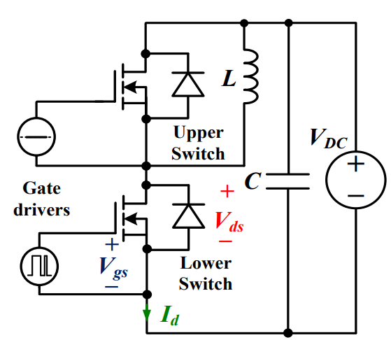
IRF830 Test Circuits
IRF830 Alternatives
8N50, FTK480, KF12N50
Where to use IRF830
IRF830 can be used in many settings. For example, it can be used in high voltage circuits, high speed applications, motor drivers and in any general purpose applications which fall under its ratings. It can also be used at the output of ICs, Microcontroller and electronic platforms as described above. Also, it can be used to build high power audio amplifiers.
IRF830 Applications
High current, high speed switching
Swith mode power supplies (smps)
DC-AC converters for welding equipment and uninterruptible power supplies and motor driver
Switching high power devices
Inverter Circuits
DC-DC Converters
Control speed of motors
LED dimmers or flashers


IRF830 Manufacturer
STMicroelectronics is a global independent semiconductor company and is a leader in developing and delivering semiconductor solutions across the spectrum of microelectronics applications. An unrivaled combination of silicon and system expertise, manufacturing strength, Intellectual Property (IP) portfolio and strategic partners positions the Company at the forefront of System-on-Chip (SoC) technology and its products play a key role in enabling today's convergence trends.
Trend Analysis
Datasheet PDF
- Datasheets :
1.What is IRF830?
The IRF830 is a fast switching high voltage N-Channel MOSFET with a low on-state resistance. The MOSFET has a maximum drain to source voltage of 500V. The MOSFET will have a drain to source internal resistance of 1.5Ω when triggered with 10V gate voltage.
2.What is IRF in Mosfet?
It is basically an N-Channel power Metal Oxide Silicon Field Effect Transistor (MOSFET) and operates in enhancement mode.
3.What is an N-channel Mosfet?
An N-Channel MOSFET is a type of MOSFET in which the channel of the MOSFET is composed of a majority of electrons as current carriers. When the MOSFET is activated and is on, the majority of the current flowing are electrons moving through the channel.
4.I'm working on a project and I need to switch IRF830 N-Channel MOSFET at roughly 100KHz as low-side. So, how much output current I need to drive this MOSFET 4 in parallel?
First, gate drive current is not typically chosen to just meet the capacitance of the MOSFET. Instead the drive is selected to move the gate voltage as quickly as necessary to maximize the switching efficiency of the circuit. This is why even small gate drivers are specified to deliver a few Amps (in a brief pulse).
Now let me answer your question. The datasheet shows Qg = 38 nC with Vgs ending at 10 V and Vds starting at 400 V. Of this 5 nC is Qgs and 22 nC is Qgd. Roughly speaking the gate driver has to drive 2 capacitors. One between Gate and Drain and one between Gate and Source. I tried a simple diagram below.
Vdrive --| Cgd |-- Drain
Vdrive --| Cgs |-- Source
The capacitance is junction and oxide capacitance so it is not constant but changes significantly -- Cgd especially -- with voltage. This is why both gate charge and gate capacitance are given.
Assume the drive is 10 V then 5 nC is put onto the gate 100 k times a second = 5 uA. For the gate charge only. The gate to drain capacitance dominates but the drain is probably not a fixed voltage so this an calculation is an estimate. With the scant information provided it's a wild guess. But 38 nC * 100 kHz = 3.8 mA.
Of course scale all this up by 4 when you put 4 FETs in parallel.
5.How to safely long run IRF830 in a Circuit?
For long life performance it is suggested to not use this transistor on its max limits. Using a component on its max limits can provide stress on a component and may result internal and outer damage of the component. Therefore we suggest using a component at least 20% below from its maximum ratings. The max drains to source current is 4.5A, therefore do not drive load more than 3.6A. The max drain to source voltage is 500V therefore d not drive load of more than 400V and always store and operate the transistor in temperature above -55 degree Celsius and below +150 degree Celsius.
 ADS1262 ADC: Feature, Pinout and Datasheet
16 August 20246421
 How to use BME280 with Arduino?
07 June 20223753
![TLP521-2XGB Optocoupler: TLP521 Series, Datasheet, Pinout [FAQ]](https://res.utmel.com/Images/Article/03d1cf24-6a28-4952-9a58-b45ee6eedbf4.jpg) TLP521-2XGB Optocoupler: TLP521 Series, Datasheet, Pinout [FAQ]
TLP521-2XGB Optocoupler: TLP521 Series, Datasheet, Pinout [FAQ]06 January 20231776
![Arduino VS Raspberry pi[Video]: How to differentiate them?](https://res.utmel.com/Images/Article/d2187b34-53c4-4a01-8c0b-c062c718249f.png) Arduino VS Raspberry pi[Video]: How to differentiate them?
Arduino VS Raspberry pi[Video]: How to differentiate them?20 April 20225114
 LM7915 Regulator IC: Equivalent, Schematic and Datasheet
14 September 20217959
 Top 5 Digital-to-Analog Converters for Industrial Applications
07 June 2025975
 AS1120 LCD Driver: Datasheet, Pinout, Application
06 September 2021386
 Unveiling the ATtiny25/45/85 Microcontroller: A Detailed Exploration
29 February 2024281
 Applications of FPGAs in Artificial Intelligence: A Comprehensive Guide
29 August 20253988
 Introduction to Temperature Sensors
24 October 20259631
 Chiplet Brings Change to the Business Model of IP Design Companies
05 September 20224256
 Introduction to PCB Layout Principles
13 November 20206845
 Resistor Symbols: From Circuit Diagrams to PCB Design
20 March 202616052
 Discovering New and Advanced Methodology for Determining the Dynamic Characterization of Wide Bandgap Devices
15 March 20242518
 TinyML Takes a Major Step Forward as Israeli Company Releases New Chip
19 April 20221098
 SEMI: Semiconductor Materials Market to Exceed US$70 Billion By 2023
27 September 20222633
STMicroelectronics
In Stock
United States
China
Canada
Japan
Russia
Germany
United Kingdom
Singapore
Italy
Hong Kong(China)
Taiwan(China)
France
Korea
Mexico
Netherlands
Malaysia
Austria
Spain
Switzerland
Poland
Thailand
Vietnam
India
United Arab Emirates
Afghanistan
Åland Islands
Albania
Algeria
American Samoa
Andorra
Angola
Anguilla
Antigua & Barbuda
Argentina
Armenia
Aruba
Australia
Azerbaijan
Bahamas
Bahrain
Bangladesh
Barbados
Belarus
Belgium
Belize
Benin
Bermuda
Bhutan
Bolivia
Bonaire, Sint Eustatius and Saba
Bosnia & Herzegovina
Botswana
Brazil
British Indian Ocean Territory
British Virgin Islands
Brunei
Bulgaria
Burkina Faso
Burundi
Cabo Verde
Cambodia
Cameroon
Cayman Islands
Central African Republic
Chad
Chile
Christmas Island
Cocos (Keeling) Islands
Colombia
Comoros
Congo
Congo (DRC)
Cook Islands
Costa Rica
Côte d’Ivoire
Croatia
Cuba
Curaçao
Cyprus
Czechia
Denmark
Djibouti
Dominica
Dominican Republic
Ecuador
Egypt
El Salvador
Equatorial Guinea
Eritrea
Estonia
Eswatini
Ethiopia
Falkland Islands
Faroe Islands
Fiji
Finland
French Guiana
French Polynesia
Gabon
Gambia
Georgia
Ghana
Gibraltar
Greece
Greenland
Grenada
Guadeloupe
Guam
Guatemala
Guernsey
Guinea
Guinea-Bissau
Guyana
Haiti
Honduras
Hungary
Iceland
Indonesia
Iran
Iraq
Ireland
Isle of Man
Israel
Jamaica
Jersey
Jordan
Kazakhstan
Kenya
Kiribati
Kosovo
Kuwait
Kyrgyzstan
Laos
Latvia
Lebanon
Lesotho
Liberia
Libya
Liechtenstein
Lithuania
Luxembourg
Macao(China)
Madagascar
Malawi
Maldives
Mali
Malta
Marshall Islands
Martinique
Mauritania
Mauritius
Mayotte
Micronesia
Moldova
Monaco
Mongolia
Montenegro
Montserrat
Morocco
Mozambique
Myanmar
Namibia
Nauru
Nepal
New Caledonia
New Zealand
Nicaragua
Niger
Nigeria
Niue
Norfolk Island
North Korea
North Macedonia
Northern Mariana Islands
Norway
Oman
Pakistan
Palau
Palestinian Authority
Panama
Papua New Guinea
Paraguay
Peru
Philippines
Pitcairn Islands
Portugal
Puerto Rico
Qatar
Réunion
Romania
Rwanda
Samoa
San Marino
São Tomé & Príncipe
Saudi Arabia
Senegal
Serbia
Seychelles
Sierra Leone
Sint Maarten
Slovakia
Slovenia
Solomon Islands
Somalia
South Africa
South Sudan
Sri Lanka
St Helena, Ascension, Tristan da Cunha
St. Barthélemy
St. Kitts & Nevis
St. Lucia
St. Martin
St. Pierre & Miquelon
St. Vincent & Grenadines
Sudan
Suriname
Svalbard & Jan Mayen
Sweden
Syria
Tajikistan
Tanzania
Timor-Leste
Togo
Tokelau
Tonga
Trinidad & Tobago
Tunisia
Turkey
Turkmenistan
Turks & Caicos Islands
Tuvalu
U.S. Outlying Islands
U.S. Virgin Islands
Uganda
Ukraine
Uruguay
Uzbekistan
Vanuatu
Vatican City
Venezuela
Wallis & Futuna
Yemen
Zambia
Zimbabwe
![STW9NK90Z]() STW9NK90Z
STW9NK90ZSTMicroelectronics
![STD20NF20]() STD20NF20
STD20NF20STMicroelectronics
![STP80NF10]() STP80NF10
STP80NF10STMicroelectronics
![STW9N150]() STW9N150
STW9N150STMicroelectronics
![STW11NK100Z]() STW11NK100Z
STW11NK100ZSTMicroelectronics
![STH3N150-2]() STH3N150-2
STH3N150-2STMicroelectronics
![STP12NM50FP]() STP12NM50FP
STP12NM50FPSTMicroelectronics
![STW45NM60]() STW45NM60
STW45NM60STMicroelectronics
![STP11NK50ZFP]() STP11NK50ZFP
STP11NK50ZFPSTMicroelectronics
![STP12NM50]() STP12NM50
STP12NM50STMicroelectronics


