

 Product
 Brand
Brand Articles
 Tools
Tools
The Comprehensive Introduction to Si53306

1 Circuit 1:4 Clock Buffer QUAD SI53306 16-VFQFN Exposed Pad
Unit Price: $3.563690
Ext Price: $3.56


1 Circuit 1:4 Clock Buffer QUAD SI53306 16-VFQFN Exposed Pad
The Si53306 comes from the Si5330x family of Universal/Any-format fanout buffers and is ideal for clock distribution (1 MHz minimum) and redundant clocking applications. This post will unlock its datasheet, features, pinout and more detailed information about Si53306.
Si53306 Pinout
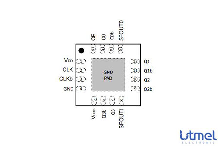
Si53306 Pinout
Si53306 CAD Model
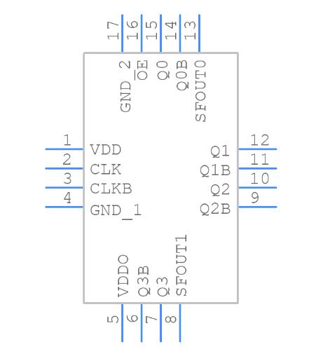
Si53306 Symbol
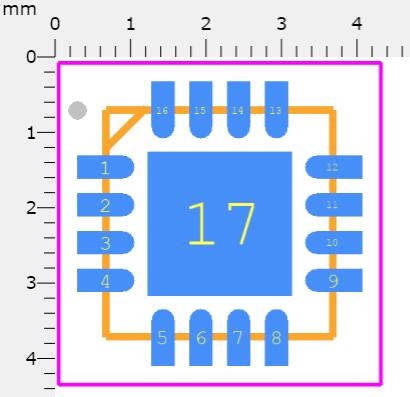
Si53306 Footprint
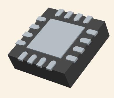
Si53306 3D Model
Si53306 Key Features
• Ultra-low additive jitter: 50 fs RMS
• Built-in LDOs for high PSRR performance
• Up to 10 outputs
• Any-format Inputs (LVPECL, Low-power LVPECL, LVDS, CML, HCSL, LVCMOS)
• Wide frequency range
• Output Enable option
• Multiple configuration options
• Dual Bank option
-2:1 Input Mux operation
-Synchronous output enable
• Loss of signal (LOS) monitors for loss of input clock
• Output clock division: /1, /2, /4
• RoHS compliant, Pb-free
• Temperature range: –40 to +85 °C
Si53306 Block Diagram
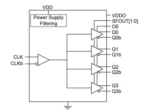
Si53306 Block Diagram
Si53306 Funtion Performance
The Si5330x family of low-jitter, low-skew, universal/any-format buffers accepts the most common differential or LVCMOS input signals. These devices are available in multiple configurations customized for the end application.
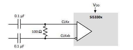
Si53306 Differential (HCSL, LVPECL, Low-Power LVPECL, LVDS, CML) AC-Coupled Input Termination
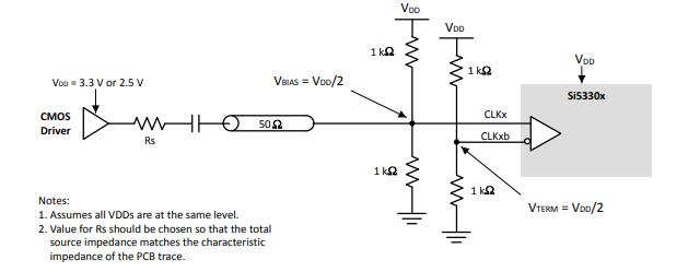
Si53306 AC-Coupled, Single-Ended (LVCMOS) Input Termination
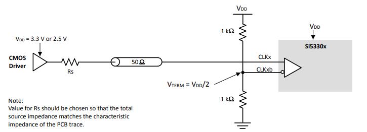
Si53306 DC-Coupled, Single-Ended (LVCMOS) Input Termination
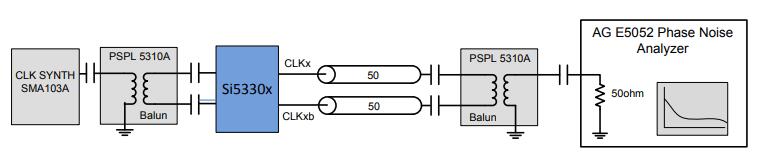
Si53306 Differential Measurement Method Using a Balun
Each of the phase noise plots superimposes Source Jitter, Total SE Jitter, and Total Diff Jitter on the same diagram.
• Source Jitter—Reference clock phase noise (measured Single-ended to PNA).
• Total Jitter (SE)—Combined source and clock buffer phase noise measured as a single-ended output to the phase noise analyzer and integrated from 12 kHz to 20 MHz.
• Total Jitter (Diff)—Combined source and clock buffer phase noise measured as a differential output to the phase noise analyzer and integrated from 12 kHz to 20 MHz. The differential measurement as shown in each figure is made using a balun.
Si53306 Package
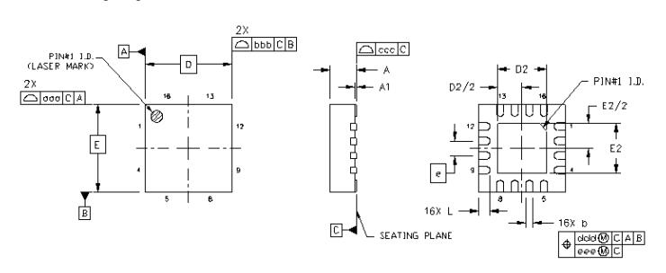
Si53306 Package
Specifications
- TypeParameter
- Factory Lead Time6 Weeks
- Mount
In electronic components, the term "Mount" typically refers to the method or process of physically attaching or fixing a component onto a circuit board or other electronic device. This can involve soldering, adhesive bonding, or other techniques to secure the component in place. The mounting process is crucial for ensuring proper electrical connections and mechanical stability within the electronic system. Different components may have specific mounting requirements based on their size, shape, and function, and manufacturers provide guidelines for proper mounting procedures to ensure optimal performance and reliability of the electronic device.
Surface Mount - Mounting Type
The "Mounting Type" in electronic components refers to the method used to attach or connect a component to a circuit board or other substrate, such as through-hole, surface-mount, or panel mount.
Surface Mount - Package / Case
refers to the protective housing that encases an electronic component, providing mechanical support, electrical connections, and thermal management.
16-VFQFN Exposed Pad - Number of Pins16
- Frequency(Max)725MHz
- Operating Temperature
The operating temperature is the range of ambient temperature within which a power supply, or any other electrical equipment, operate in. This ranges from a minimum operating temperature, to a peak or maximum operating temperature, outside which, the power supply may fail.
-40°C~85°C - Packaging
Semiconductor package is a carrier / shell used to contain and cover one or more semiconductor components or integrated circuits. The material of the shell can be metal, plastic, glass or ceramic.
Tape & Reel (TR) - Published1997
- JESD-609 Code
The "JESD-609 Code" in electronic components refers to a standardized marking code that indicates the lead-free solder composition and finish of electronic components for compliance with environmental regulations.
e3 - Part Status
Parts can have many statuses as they progress through the configuration, analysis, review, and approval stages.
Active - Moisture Sensitivity Level (MSL)
Moisture Sensitivity Level (MSL) is a standardized rating that indicates the susceptibility of electronic components, particularly semiconductors, to moisture-induced damage during storage and the soldering process, defining the allowable exposure time to ambient conditions before they require special handling or baking to prevent failures
2 (1 Year) - Number of Terminations16
- TypeFanout Buffer (Distribution), Translator
- Terminal Finish
Terminal Finish refers to the surface treatment applied to the terminals or leads of electronic components to enhance their performance and longevity. It can improve solderability, corrosion resistance, and overall reliability of the connection in electronic assemblies. Common finishes include nickel, gold, and tin, each possessing distinct properties suitable for various applications. The choice of terminal finish can significantly impact the durability and effectiveness of electronic devices.
Matte Tin (Sn) - Voltage - Supply
Voltage - Supply refers to the range of voltage levels that an electronic component or circuit is designed to operate with. It indicates the minimum and maximum supply voltage that can be applied for the device to function properly. Providing supply voltages outside this range can lead to malfunction, damage, or reduced performance. This parameter is critical for ensuring compatibility between different components in a circuit.
1.71V~3.63V - Terminal Position
In electronic components, the term "Terminal Position" refers to the physical location of the connection points on the component where external electrical connections can be made. These connection points, known as terminals, are typically used to attach wires, leads, or other components to the main body of the electronic component. The terminal position is important for ensuring proper connectivity and functionality of the component within a circuit. It is often specified in technical datasheets or component specifications to help designers and engineers understand how to properly integrate the component into their circuit designs.
QUAD - Terminal Form
Occurring at or forming the end of a series, succession, or the like; closing; concluding.
NO LEAD - Terminal Pitch
The center distance from one pole to the next.
0.5mm - Base Part Number
The "Base Part Number" (BPN) in electronic components serves a similar purpose to the "Base Product Number." It refers to the primary identifier for a component that captures the essential characteristics shared by a group of similar components. The BPN provides a fundamental way to reference a family or series of components without specifying all the variations and specific details.
SI53306 - Output
In electronic components, the parameter "Output" typically refers to the signal or data that is produced by the component and sent to another part of the circuit or system. The output can be in the form of voltage, current, frequency, or any other measurable quantity depending on the specific component. The output of a component is often crucial in determining its functionality and how it interacts with other components in the circuit. Understanding the output characteristics of electronic components is essential for designing and troubleshooting electronic circuits effectively.
CML, HCSL, LVCMOS, LVDS, LVPECL - Qualification Status
An indicator of formal certification of qualifications.
Not Qualified - Number of Circuits1
- Nominal Supply Current
Nominal current is the same as the rated current. It is the current drawn by the motor while delivering rated mechanical output at its shaft.
55mA - Quiescent Current
The quiescent current is defined as the current level in the amplifier when it is producing an output of zero.
100mA - Logic Function
In electronic components, the term "Logic Function" refers to the specific operation or behavior of a component based on its input signals. It describes how the component processes the input signals to produce the desired output. Logic functions are fundamental to digital circuits and are used to perform logical operations such as AND, OR, NOT, and XOR.Each electronic component, such as logic gates or flip-flops, is designed to perform a specific logic function based on its internal circuitry. By understanding the logic function of a component, engineers can design and analyze complex digital systems to ensure proper functionality and performance. Different logic functions can be combined to create more complex operations, allowing for the creation of sophisticated digital devices and systems.
Translator - Input
In electronic components, "Input" refers to the signal or data that is provided to a device or system for processing or manipulation. It is the information or command that is received by the component to initiate a specific function or operation. The input can come from various sources such as sensors, other electronic devices, or user interactions. It is crucial for the proper functioning of the component as it determines how the device will respond or behave based on the input received. Understanding and managing the input parameters is essential in designing and using electronic components effectively.
CML, HCSL, LVCMOS, LVDS, LVPECL - Ratio - Input:Output
The parameter "Ratio - Input:Output" in electronic components refers to the relationship between the input and output quantities of a device or system. It is a measure of how the input signal or energy is transformed or converted into the output signal or energy. This ratio is often expressed as a numerical value or percentage, indicating the efficiency or effectiveness of the component in converting the input to the desired output. A higher ratio typically signifies better performance or higher efficiency, while a lower ratio may indicate losses or inefficiencies in the conversion process. Understanding and optimizing the input-output ratio is crucial in designing and evaluating electronic components for various applications.
1:4 - Differential - Input:Output
Differential - Input:Output refers to the relationship between the input and output signals in differential amplifiers or circuits. It measures the difference in voltage between two input terminals and produces an output that is proportional to this difference. This parameter is essential for noise rejection and improving signal integrity in various applications, such as operational amplifiers and data acquisition systems. It allows circuits to effectively amplify small signals while minimizing interference and common-mode noise.
Yes/Yes - Prop. Delay@Nom-Sup
The parameter "Prop. Delay@Nom-Sup" in electronic components refers to the propagation delay at nominal supply voltage. Propagation delay is the time it takes for a signal to travel from the input of a component to the output, typically measured in nanoseconds or picoseconds. The nominal supply voltage is the standard operating voltage specified for the component.This parameter is important because it affects the overall speed and performance of the electronic circuit. A shorter propagation delay means faster signal processing and better overall performance. Designers need to consider the propagation delay at the nominal supply voltage when selecting components for their circuits to ensure proper functionality and meet performance requirements.
0.825 ns - RoHS Status
RoHS means “Restriction of Certain Hazardous Substances” in the “Hazardous Substances Directive” in electrical and electronic equipment.
RoHS Compliant
Parts with Similar Specs
- ImagePart NumberManufacturerPackage / CaseNumber of PinsNumber of CircuitsLogic FunctionFrequency (Max)Quiescent CurrentMountView Compare
![SI53306-B-GMR]()
SI53306-B-GMR
16-VFQFN Exposed Pad
16
1
Translator
725MHz
100 mA
Surface Mount
![5PB1106CMGI]()
16-VFQFN Exposed Pad
16
1
Clock
-
-
Surface Mount
![SY89833ALMG]()
16-VFQFN Exposed Pad
16
1
-
725MHz
-
Surface Mount
![SI53307-B-GM]()
16-VFQFN Exposed Pad, 16-MLF?
16
1
-
2GHz
100 mA
Surface Mount
![SI53340-B-GM]()
QFN
16
1
-
200 MHz
-
Surface Mount


Conclusion
The Si5330x family is available in multiple configurations, with some versions offering a selectable input clock using a 2:1 input mux. Other features include an independent (synchronous) output enable, glitchless switching, LOS monitor of input clocks, output clock division, and built-in format translation. These buffers can be paired with the Si534x clocks and jitter attenuators, the Si5332 clocks, and the Si5xx oscillators to deliver end-to-end clock tree performance
Datasheet PDF
- Datasheets :
- PCN Design/Specification :
- PCN Other :
 Guide to onsemi MBRS360T3G Datasheets
19 August 2025289
 LM1084 Positive Regulators : Price, Application and Circuit
31 July 20213911
 AO3401A P-Channel 30V Fast Switching MOSFETs, 4A SOT23 and AO3401A Equivalents
08 February 202211546
 MOC3052 Photocoupler: Datasheet, Alternatives and Pinout
16 August 20218559
 HMC344LC3TR-R5 RF Switch: Pinout, Feature, Datasheet
14 August 2024550
 CS4270 Stereo Audio CODEC: CS4270 Datasheet, Pinout, CS4272 VS. CS4270
02 March 20224397
 ULN2004A Darlington Array: Pinout, Equivalent and Datasheet
29 November 20217742
 2N5952 N-Channel RFAmplifier: Equivalent, Pinout, Datasheet
10 January 20222893
 How to Design Reliable High-Side Switching Circuits with P-Channel MOSFETs?
22 July 202514698
 Chip Packaging Lead Time Has Grown to 50 Weeks
07 April 20226313
 Microcontroller (MCU) Market Analysis
09 February 20226560
 Insulation Approaches for Power Electronic Converters
12 October 20234769
 How to Use the Oscilloscope's X-Y Display Correctly
19 September 202216634
 Introduction To Different Types Of Relays
10 November 202020817
 Volkswagen CFO: Chip Supply Shortage Will Continue Until 2024
11 April 20224985
 Introduction to AC motor
05 March 20219926
Silicon Labs
In Stock
Minimum: 1 Multiples: 1
Qty
Unit Price
Ext Price
1
$3.563690
$3.56
10
$3.361972
$33.62
100
$3.171671
$317.17
500
$2.992143
$1,496.07
1000
$2.822776
$2,822.78
Not the price you want? Send RFQ Now and we'll contact you ASAP.
Inquire for More Quantity
![SI5330F-B00214-GM]() SI5330F-B00214-GM
SI5330F-B00214-GMSilicon Labs
![SI53306-B-GM]() SI53306-B-GM
SI53306-B-GMSilicon Labs
![SI53302-B-GM]() SI53302-B-GM
SI53302-B-GMSilicon Labs
![SI53301-B-GMR]() SI53301-B-GMR
SI53301-B-GMRSilicon Labs
![SI5330G-B00217-GM]() SI5330G-B00217-GM
SI5330G-B00217-GMSilicon Labs
![SI53304-B-GM]() SI53304-B-GM
SI53304-B-GMSilicon Labs
![SI53305-B-GM]() SI53305-B-GM
SI53305-B-GMSilicon Labs
![SI5330M-B00231-GM]() SI5330M-B00231-GM
SI5330M-B00231-GMSilicon Labs
![SI5330B-B00205-GMR]() SI5330B-B00205-GMR
SI5330B-B00205-GMRSilicon Labs


