
LM324 vs LM358 : Which one is better?

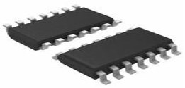
4 Channels 40mA per Channel 45nA 65 dB Instrumentational OP Amps 0.5μA 16V 3V~32V ±1.5V~16V LM324 14 Pins 14-SOIC (0.154, 3.90mm Width)


4 Channels 40mA per Channel 45nA 65 dB Instrumentational OP Amps 0.5μA 16V 3V~32V ±1.5V~16V LM324 14 Pins 14-SOIC (0.154, 3.90mm Width)
The LM124 consists of four independent, high-gain, internally frequency compensated operational amplifiers designed to operate from a single power supply over a wide range of voltages. The LM358 is made using two internally compensated, two−stage operational amplifiers. This article is going to cover the differences between LM124 and LM358 from the perspective of description, absolute maximum ratings, features, electrical characteristics, and more details.

dạy sửa main nguồn 1.05 1. 8 pch IC LM324 LM358 giga h61mds23.0
LM124 Description
The LM124 consists of four independent, high-gain, internally frequency compensated operational amplifiers designed to operate from a single power supply over a wide range of voltages. Operation from split-power supplies is also possible and the low-power supply current drain is independent of the magnitude of the power supply voltage.
Application areas include transducer amplifiers, DC gain blocks, and all the conventional op-amp circuits which now can be more easily implemented in single power supply systems. For example, the LM124 can directly operate off of the standard 5 -V power supply voltage which is used in digital systems, and easily provides the required interface electronics without requiring the additional ±15 V power supplies.
LM358 Description
The LM358 is equivalent to one−half of an LM324. These amplifiers have several distinct advantages over standard operational amplifier types in single supply applications. They can operate at supply voltages as low as 3.0 V or as high as 32 V, with quiescent currents about one−fifth of those associated with the MC1741 (on a per amplifier basis). The common-mode input range includes the negative supply, thereby eliminating the necessity for external biasing components in many applications. The output voltage range also includes the negative power supply voltage.
Comparison of Absolute Maximum Ratings of the LM324 vs LM358
| LM124-N/LM224-N/LM324-N LM124A/LM224A/LM324A | LM2902-N | ||||||
| MIN | MAX | MIN | MAX | UNIT | |||
| Supply Voltage, V+ | 32 | 26 | V | ||||
| Differential Input Voltage | 32 | 26 | V | ||||
| Input Voltage | −0.3 | 32 | −0.3 | 26 | V | ||
| Input Current (VIN < −0.3 V)(3) | 50 | 50 | mA | ||||
| Power Dissipation(4) | PDIP | 1130 | 1130 | mW | |||
| CDIP | 1260 | 1260 | mW | ||||
| SOIC Package | 800 | 800 | mW | ||||
| Output Short-Circuit to GND (One Amplifier) (5) | V+ ≤ 15 V and TA = 25°C | Continuous | Continuous | ||||
| Lead Temperature (Soldering, 10 seconds) | 260 | 260 | °C | ||||
| Soldering Information | Dual-In-Line Package | Soldering (10 seconds) | 260 | 260 | °C | ||
| Small Outline Package | Vapor Phase (60 seconds) | 215 | 215 | °C | |||
| Infrared (15 seconds) | 220 | 220 | °C | ||||
| Storage temperature, Tstg | –65 | 150 | –65 | 150 | °C | ||
LM324 Absolute Maximum Ratings
| Rating | Symbol | Value | Unit |
| Power Supply Voltages Split Supplies Single Supply | VCC VCC, VEE | 32 ±16 | Vdc |
| Input Differential Voltage Range (Note 1) | VIDR | ±32 | Vdc |
| Input Common-Mode Voltage Range | VICR | −0.3 to 32 | Vdc |
| Output Short Circuit Duration | tSC | Continuous | |
| Junction Temperature | TJ | 150 | °C |
| Thermal Resistance, Junction−to−Air (Note 2) Case 846A Case 751 Case 626 | RθJA | 238 212 161 | ° C/W |
| Storage Temperature Range | Tstg | −65 to +150 | °C |
| Operating Ambient Temperature Range LM258 LM358, LM358A, LM358E LM2904, LM2904A, LM2904E LM2904V, NCV2904 (Note 3) | TA | −25 to +85 0 to +70 −40 to +105 −40 to +125 | °C |
LM358 Absolute Maximum Ratings
Comparison of features of the LM324 vs LM358
Features of the LM324 include the following:
Internally Frequency Compensated for Unity Gain
Large DC Voltage Gain100 dB
Wide Bandwidth (Unity Gain) 1 MHz
(Temperature Compensated)
Wide Power Supply Range:
– Single Supply 3 V to 32 V
– or Dual Supplies ±1.5 V to ±16 V
Very Low Supply Current Drain(700 μA)
—Essentially Independent of Supply Voltage
Low Input Biasing Current45 nA
(Temperature Compensated)
Low Input Offset Voltage 2 mV
and Offset Current: 5 nA
Input Common-Mode Voltage Range Includes
Ground
Differential Input Voltage Range Equal to the
Power Supply Voltage
Large Output Voltage Swing0 V to V +− 1.5 V
Features of the LM358 include the following:
Short circuit protected Outputs
True Differential Input Stage
Single Supply Operation: 3.0 V to 32 V
Low Input Bias Currents
Internally Compensated
Common Mode Range Extends to Negative Supply
Single and Split Supply Operation
ESDClamps on the Inputs Increase Ruggedness of the Device
without Affecting Operation
NCVPrefix for Automotive and Other Applications Requiring
Unique Site and Control Change Requirements; AEC−Q100
Qualified and PPAP Capable
These Devices are Pb−Free, Halogen Free/BFRFree, and are RoHS
Compliant
Comparison of Electrical Characteristics of the LM324 vs LM358
| PARAMETER | TEST CONDITIONS | LM124A | LM224A | LM324A | UNIT | |||||||
| MIN | TYP | MAX | MIN | TYP | MAX | MIN | TYP | MAX | ||||
| Input Offset Voltage | TA = 25°C(2) | 1 | 2 | 1 | 3 | 2 | 3 | mV | ||||
| Input Bias Current(3) | IIN(+) or IIN(−), VCM = 0 V, TA = 25°C | 20 | 50 | 40 | 80 | 45 | 100 | nA | ||||
| Input Offset Current | IIN(+) or IIN(−), VCM = 0 V, TA = 25°C | 2 | 10 | 2 | 15 | 5 | 30 | nA | ||||
| Input Common-Mode Voltage Range(4) | V+ = 30 V, (LM2902-N, V+ = 26 V), TA = 25°C | 0 | V+−1.5 | 0 | V+−1.5 | 0 | V+−1.5 | V | ||||
| Supply Current | Over Full Temperature Range, RL = ∞ On All Op Amps V+ = 30 V (LM2902-N V+ = 26 V) | 1.5 3 | 1.5 3 | 1.5 3 | mA | |||||||
| V+ = 5 V | 0.7 | 1.2 | 0.7 | 1.2 | 0.7 | 1.2 | ||||||
| Large Signal Voltage Gain | V+ = 15 V, RL≥ 2 kΩ, (VO = 1 V to 11 V), TA = 25°C | 50 | 100 | 50 | 100 | 25 | 100 | V/mV | ||||
| Common-Mode Rejection Ratio | DC, VCM = 0 V to V+ − 1.5 V, TA = 25°C | 70 | 85 | 70 | 85 | 65 | 85 | dB | ||||
| Power Supply Rejection Ratio | V+ = 5 V to 30 V, (LM2902-N, V+ = 5V to 26 V), TA = 25°C | 65 | 100 | 65 | 100 | 65 | 100 | dB | ||||
| Amplifier-to-Amplifier Coupling(5) | f = 1 kHz to 20 kHz, TA = 25°C, (Input Referred) | −120 | −120 | −120 | dB | |||||||
| Output Current | Source | V + = 1 V, V − = 0 V, IN IN V+ = 15 V, VO = 2 V, TA = 25°C | 20 | 40 | 20 | 40 | 20 | 40 | mA | |||
| Sink | V − = 1 V, V + = 0 V, IN IN V+ = 15 V, VO = 2 V, TA = 25°C | 10 | 20 | 10 | 20 | 10 | 20 | μA | ||||
| V − = 1 V, V + = 0 V, IN IN V+ = 15 V, VO = 200 mV, TA = 25°C | 12 | 50 | 12 | 50 | 12 | 50 | ||||||
| Short Circuit to Ground | V+ = 15 V, TA = 25°C(6) | 40 | 60 | 40 | 60 | 40 | 60 | mA | ||||
| Input Offset Voltage | See(2) | 4 | 4 | 5 | mV | |||||||
| VOS Drift | RS = 0 Ω | 7 | 20 | 7 | 20 | 7 | 30 | μV/°C | ||||
| Input Offset Current | IIN(+) − IIN(−), VCM = 0 V | 30 | 30 | 75 | nA | |||||||
LM324 Electrical Characteristics
| Characteristic | Symbol | LM258 | LM358, LM358E | LM358A | Unit | ||||||
| Min | Typ | Max | Min | Typ | Max | Min | Typ | Max | |||
| Input Offset Voltage VCC = 5.0 V to 30 V, VIC = 0 V to VCC −1.7 V, VO 1.4 V, RS = 0 Ω TA = 25°C TA = Thigh (Note 4) TA = Tlow (Note 4) | VIO | mV | |||||||||
| − | 2 | 5 | − | 2 | 7 | − | 2 | 3 | |||
| − | − | 7 | − | − | 9 | − | − | 5 | |||
| − | − | 7 | − | − | 9 | − | − | 5 | |||
| Average Temperature Coefficient of Input Offset Voltage TA = Thigh to Tlow (Note 4) | ΔVIO/ΔT | − | 7 | − | − | 7 | − | − | 7 | − | µV/°C |
| Input Offset Current TA = Thigh to Tlow (Note 4) Input Bias Current TA = Thigh to Tlow (Note 4) | IIO IIB | − | 3 | 30 | − | 5 | 50 | − | 5 | 30 | nA |
| − | − | 100 | − | − | 150 | − | − | 75 | |||
| − | −45 | −150 | − | −45 | −250 | − | −45 | −100 | |||
| − | −50 | −300 | − | −50 | −500 | − | −50 | −200 | |||
| Average Temperature Coefficient of Input Offset Current TA = Thigh to Tlow (Note 4) | ΔIIO/ΔT | − | 10 | − | − | 10 | − | − | 10 | − | pA/°C |
| Input Common Mode Voltage Range (Note 5), VCC = 30 V VCC = 30 V, TA = Thigh to Tlow | VICR | 0 | − | 28.3 | 0 | − | 28.3 28 | 0 | − | 28.5 28 | V |
| 0 | − | 28 | 0 | − | 0 | − | |||||
| Differential Input Voltage Range | VIDR | − | − | VCC | − | − | VCC | − | − | VCC | V |
| Large Signal Open Loop Voltage Gain RL = 2.0 kΩ, VCC = 15 V, For Large VO Swing, TA = Thigh to Slow (Note 4) | AVOL | 50 25 | V/mV | ||||||||
| 100 | − | 25 | 100 | − | 25 | 100 | − | ||||
| − | − | 15 | − | − | 15 | − | − | ||||
| Channel Separation 1.0 kHz £ f £ 20 kHz, Input Referenced | CS | − | −120 | − | − | −120 | − | − | −120 | − | dB |
| Common Mode Rejection RS £ 10 kΩ | CMR | 70 | 85 | − | 65 | 70 | − | 65 | 70 | − | dB |
| Power Supply Rejection | PSR | 65 | 100 | − | 65 | 100 | − | 65 | 100 | − | dB |
| Output Voltage−High Limit TA = Thigh to Tlow (Note 4) VCC = 5.0 V, RL = 2.0 kΩ, TA = 25°C VCC = 30 V, RL = 2.0 kΩ VCC = 30 V, RL = 10 kΩ | VOH | 3.3 26 27 | 3.5 − 28 | − − − | 3.3 26 27 | 3.5 − 28 | − − − | 3.3 26 27 | 3.5 − 28 | − − − | V |
| Output Voltage−Low Limit VCC = 5.0 V, RL = 10 kΩ, TA = Thigh to Tlow (Note 4) | VOL | − | 5 | 20 | − | 5 | 20 | − | 5 | 20 | mV |
| Output Source Current VID = +1.0 V, VCC = 15 V TA = Thigh to Tlow (LM358A Only) | IO + | mA | |||||||||
| 20 | 40 | − | 20 | 40 | − | 20 | 40 | − | |||
| 10 | − | − | |||||||||
| Output Sink Current VID = −1.0 V, VCC = 15 V TA = Thigh to Tlow (LM358A Only) VID = −1.0 V, VO = 200 mV | IO − | 10 12 | 20 50 | mA mA µA | |||||||
| − | 10 | 20 | − | 10 | 20 | − | |||||
| 5 | − | − | |||||||||
| − | 12 | 50 | − | 12 | 50 | − | |||||
| Output Short Circuit to Ground (Note 6) | ISC | − | 40 | 60 | − | 40 | 60 | − | 40 | 60 | mA |
| Power Supply Current (Total Device) TA = Thigh to Tlow (Note 4) VCC = 30 V, VO = 0 V, RL = ¥ VCC = 5 V, VO = 0 V, RL = ¥ | ICC | mA | |||||||||
| − | 1.5 | 3 | − | 1.5 | 3 | − | 1.5 | 2 | |||
| − | 0.7 | 1.2 | − | 0.7 | 1.2 | − | 0.7 | 1.2 | |||
LM358 Electrical Characteristics
Specifications
- TypeParameter
- Lifecycle Status
Lifecycle Status refers to the current stage of an electronic component in its product life cycle, indicating whether it is active, obsolete, or transitioning between these states. An active status means the component is in production and available for purchase. An obsolete status indicates that the component is no longer being manufactured or supported, and manufacturers typically provide a limited time frame for support. Understanding the lifecycle status is crucial for design engineers to ensure continuity and reliability in their projects.
NRND (Last Updated: 3 days ago) - Mount
In electronic components, the term "Mount" typically refers to the method or process of physically attaching or fixing a component onto a circuit board or other electronic device. This can involve soldering, adhesive bonding, or other techniques to secure the component in place. The mounting process is crucial for ensuring proper electrical connections and mechanical stability within the electronic system. Different components may have specific mounting requirements based on their size, shape, and function, and manufacturers provide guidelines for proper mounting procedures to ensure optimal performance and reliability of the electronic device.
Surface Mount - Mounting Type
The "Mounting Type" in electronic components refers to the method used to attach or connect a component to a circuit board or other substrate, such as through-hole, surface-mount, or panel mount.
Surface Mount - Package / Case
refers to the protective housing that encases an electronic component, providing mechanical support, electrical connections, and thermal management.
14-SOIC (0.154, 3.90mm Width) - Number of Pins14
- Operating Temperature
The operating temperature is the range of ambient temperature within which a power supply, or any other electrical equipment, operate in. This ranges from a minimum operating temperature, to a peak or maximum operating temperature, outside which, the power supply may fail.
0°C~70°C - Packaging
Semiconductor package is a carrier / shell used to contain and cover one or more semiconductor components or integrated circuits. The material of the shell can be metal, plastic, glass or ceramic.
Tube - JESD-609 Code
The "JESD-609 Code" in electronic components refers to a standardized marking code that indicates the lead-free solder composition and finish of electronic components for compliance with environmental regulations.
e0 - Part Status
Parts can have many statuses as they progress through the configuration, analysis, review, and approval stages.
Not For New Designs - Moisture Sensitivity Level (MSL)
Moisture Sensitivity Level (MSL) is a standardized rating that indicates the susceptibility of electronic components, particularly semiconductors, to moisture-induced damage during storage and the soldering process, defining the allowable exposure time to ambient conditions before they require special handling or baking to prevent failures
1 (Unlimited) - Number of Terminations14
- ECCN Code
An ECCN (Export Control Classification Number) is an alphanumeric code used by the U.S. Bureau of Industry and Security to identify and categorize electronic components and other dual-use items that may require an export license based on their technical characteristics and potential for military use.
EAR99 - Terminal Finish
Terminal Finish refers to the surface treatment applied to the terminals or leads of electronic components to enhance their performance and longevity. It can improve solderability, corrosion resistance, and overall reliability of the connection in electronic assemblies. Common finishes include nickel, gold, and tin, each possessing distinct properties suitable for various applications. The choice of terminal finish can significantly impact the durability and effectiveness of electronic devices.
Tin/Lead (Sn/Pb) - Max Power Dissipation
The maximum power that the MOSFET can dissipate continuously under the specified thermal conditions.
800mW - Terminal Position
In electronic components, the term "Terminal Position" refers to the physical location of the connection points on the component where external electrical connections can be made. These connection points, known as terminals, are typically used to attach wires, leads, or other components to the main body of the electronic component. The terminal position is important for ensuring proper connectivity and functionality of the component within a circuit. It is often specified in technical datasheets or component specifications to help designers and engineers understand how to properly integrate the component into their circuit designs.
DUAL - Terminal Form
Occurring at or forming the end of a series, succession, or the like; closing; concluding.
GULL WING - Peak Reflow Temperature (Cel)
Peak Reflow Temperature (Cel) is a parameter that specifies the maximum temperature at which an electronic component can be exposed during the reflow soldering process. Reflow soldering is a common method used to attach electronic components to a circuit board. The Peak Reflow Temperature is crucial because it ensures that the component is not damaged or degraded during the soldering process. Exceeding the specified Peak Reflow Temperature can lead to issues such as component failure, reduced performance, or even permanent damage to the component. It is important for manufacturers and assemblers to adhere to the recommended Peak Reflow Temperature to ensure the reliability and functionality of the electronic components.
235 - Number of Functions4
- Supply Voltage
Supply voltage refers to the electrical potential difference provided to an electronic component or circuit. It is crucial for the proper operation of devices, as it powers their functions and determines performance characteristics. The supply voltage must be within specified limits to ensure reliability and prevent damage to components. Different electronic devices have specific supply voltage requirements, which can vary widely depending on their design and intended application.
5V - Terminal Pitch
The center distance from one pole to the next.
1.27mm - Base Part Number
The "Base Part Number" (BPN) in electronic components serves a similar purpose to the "Base Product Number." It refers to the primary identifier for a component that captures the essential characteristics shared by a group of similar components. The BPN provides a fundamental way to reference a family or series of components without specifying all the variations and specific details.
LM324 - Pin Count
a count of all of the component leads (or pins)
14 - Operating Supply Voltage
The voltage level by which an electrical system is designated and to which certain operating characteristics of the system are related.
16V - Power Supplies
an electronic circuit that converts the voltage of an alternating current (AC) into a direct current (DC) voltage.?
5/30V - Number of Channels4
- Operating Supply Current
Operating Supply Current, also known as supply current or quiescent current, is a crucial parameter in electronic components that indicates the amount of current required for the device to operate under normal conditions. It represents the current drawn by the component from the power supply while it is functioning. This parameter is important for determining the power consumption of the component and is typically specified in datasheets to help designers calculate the overall power requirements of their circuits. Understanding the operating supply current is essential for ensuring proper functionality and efficiency of electronic systems.
1.5mA - Nominal Supply Current
Nominal current is the same as the rated current. It is the current drawn by the motor while delivering rated mechanical output at its shaft.
1.5mA - Power Dissipation
the process by which an electronic or electrical device produces heat (energy loss or waste) as an undesirable derivative of its primary action.
800mW - Output Current
The rated output current is the maximum load current that a power supply can provide at a specified ambient temperature. A power supply can never provide more current that it's rated output current unless there is a fault, such as short circuit at the load.
40mA - Max Supply Current
Max Supply Current refers to the maximum amount of electrical current that a component can draw from its power supply under normal operating conditions. It is a critical parameter that ensures the component operates reliably without exceeding its thermal limits or damaging internal circuitry. Exceeding this current can lead to overheating, performance degradation, or failure of the component. Understanding this parameter is essential for designing circuits that provide adequate power while avoiding overload situations.
1.2mA - Slew Rate
the maximum rate of output voltage change per unit time.
0.5V/μs - Architecture
In electronic components, the parameter "Architecture" refers to the overall design and structure of the component. It encompasses the arrangement of internal components, the layout of circuitry, and the physical form of the component. The architecture of an electronic component plays a crucial role in determining its functionality, performance, and compatibility with other components in a system. Different architectures can result in variations in power consumption, speed, size, and other key characteristics of the component. Designers often consider the architecture of electronic components carefully to ensure optimal performance and integration within a larger system.
VOLTAGE-FEEDBACK - Amplifier Type
Amplifier Type refers to the classification or categorization of amplifiers based on their design, functionality, and characteristics. Amplifiers are electronic devices that increase the amplitude of a signal, such as voltage or current. The type of amplifier determines its specific application, performance capabilities, and operating characteristics. Common types of amplifiers include operational amplifiers (op-amps), power amplifiers, audio amplifiers, and radio frequency (RF) amplifiers. Understanding the amplifier type is crucial for selecting the right component for a particular circuit or system design.
General Purpose - Common Mode Rejection Ratio
Common Mode Rejection Ratio (CMRR) is a measure of the ability of a differential amplifier to reject input signals that are common to both input terminals. It is defined as the ratio of the differential gain to the common mode gain. A high CMRR indicates that the amplifier can effectively eliminate noise and interference that affects both inputs simultaneously, enhancing the fidelity of the amplified signal. CMRR is typically expressed in decibels (dB), with higher values representing better performance in rejecting common mode signals.
65 dB - Current - Input Bias
The parameter "Current - Input Bias" in electronic components refers to the amount of current required at the input terminal of a device to maintain proper operation. It is a crucial specification as it determines the minimum input current needed for the component to function correctly. Input bias current can affect the performance and accuracy of the device, especially in precision applications where small signal levels are involved. It is typically specified in datasheets for operational amplifiers, transistors, and other semiconductor devices to provide users with important information for circuit design and analysis.
45nA - Voltage - Supply, Single/Dual (±)
The parameter "Voltage - Supply, Single/Dual (±)" in electronic components refers to the power supply voltage required for the proper operation of the component. This parameter indicates whether the component requires a single power supply voltage (e.g., 5V) or a dual power supply voltage (e.g., ±15V). For components that require a single power supply voltage, only one voltage level is needed for operation. On the other hand, components that require a dual power supply voltage need both positive and negative voltage levels to function correctly.Understanding the voltage supply requirements of electronic components is crucial for designing and integrating them into circuits to ensure proper functionality and prevent damage due to incorrect voltage levels.
3V~32V ±1.5V~16V - Output Current per Channel
Output Current per Channel is a specification commonly found in electronic components such as amplifiers, audio interfaces, and power supplies. It refers to the maximum amount of electrical current that can be delivered by each individual output channel of the component. This parameter is important because it determines the capacity of the component to drive connected devices or loads. A higher output current per channel means the component can deliver more power to connected devices, while a lower output current may limit the performance or functionality of the component in certain applications. It is crucial to consider the output current per channel when selecting electronic components to ensure they can meet the power requirements of the intended system or setup.
40mA - Input Offset Voltage (Vos)
Input Offset Voltage (Vos) is a key parameter in electronic components, particularly in operational amplifiers. It refers to the voltage difference that must be applied between the two input terminals of the amplifier to nullify the output voltage when the input terminals are shorted together. In simpler terms, it represents the voltage required to bring the output of the amplifier to zero when there is no input signal present. Vos is an important parameter as it can introduce errors in the output signal of the amplifier, especially in precision applications where accuracy is crucial. Minimizing Vos is essential to ensure the amplifier operates with high precision and accuracy.
7mV - Bandwidth
In electronic components, "Bandwidth" refers to the range of frequencies over which the component can effectively operate or pass signals without significant loss or distortion. It is a crucial parameter for devices like amplifiers, filters, and communication systems. The bandwidth is typically defined as the difference between the upper and lower frequencies at which the component's performance meets specified criteria, such as a certain level of signal attenuation or distortion. A wider bandwidth indicates that the component can handle a broader range of frequencies, making it more versatile for various applications. Understanding the bandwidth of electronic components is essential for designing and optimizing circuits to ensure proper signal transmission and reception within the desired frequency range.
1MHz - Unity Gain BW-Nom
Unity Gain Bandwidth, often abbreviated as Unity Gain BW or UGBW, refers to the frequency at which an amplifier can provide a gain of one (0 dB). It is a critical parameter in assessing the performance of operational amplifiers and other amplifying devices, indicating the range of frequencies over which the amplifier can operate without distortion. Unity Gain BW is particularly important in applications where signal fidelity is crucial, as it helps determine the maximum frequency of operation for a given gain level. As the gain is reduced, the bandwidth typically increases, ensuring that the amplifier can still operate effectively across various signal frequencies.
1000 kHz - Voltage Gain
Voltage gain is a measure of how much an electronic component or circuit amplifies an input voltage signal to produce an output voltage signal. It is typically expressed as a ratio or in decibels (dB). A higher voltage gain indicates a greater amplification of the input signal. Voltage gain is an important parameter in amplifiers, where it determines the level of amplification provided by the circuit. It is calculated by dividing the output voltage by the input voltage and is a key factor in determining the overall performance and functionality of electronic devices.
100dB - Average Bias Current-Max (IIB)
The parameter "Average Bias Current-Max (IIB)" in electronic components refers to the maximum average bias current that the component can handle without exceeding its specified operating limits. Bias current is the current that flows through a component when it is in its quiescent state or when it is not actively processing a signal. Exceeding the maximum average bias current can lead to overheating, reduced performance, or even damage to the component. Therefore, it is important to ensure that the bias current does not exceed the specified maximum value to maintain the reliability and longevity of the electronic component.
0.5μA - Power Supply Rejection Ratio (PSRR)
Power Supply Rejection Ratio (PSRR) is a measure of how well an electronic component, such as an operational amplifier or voltage regulator, can reject changes in its supply voltage. It indicates the ability of the component to maintain a stable output voltage despite fluctuations in the input supply voltage. A higher PSRR value signifies better performance in rejecting noise and variations from the power supply, leading to improved signal integrity and more reliable operation in electronic circuits. PSRR is typically expressed in decibels (dB).
65dB - Low-Offset
Low-offset is a parameter used to describe the level of offset voltage in electronic components, particularly in operational amplifiers. Offset voltage refers to the small voltage difference that exists between the input terminals of the amplifier when the input voltage is zero. A low-offset value indicates that this voltage difference is minimal, which is desirable for accurate signal processing and amplification. Components with low-offset specifications are preferred in applications where precision and accuracy are critical, such as in instrumentation and measurement systems. Minimizing offset voltage helps reduce errors and ensures the faithful reproduction of input signals by the amplifier.
NO - Frequency Compensation
Frequency compensation is implemented by modifying the gain and phase characteristics of the amplifier's open loop output or of its feedback network, or both, in such a way as to avoid the conditions leading to oscillation. This is usually done by the internal or external use of resistance-capacitance networks.
YES - Supply Voltage Limit-Max
The parameter "Supply Voltage Limit-Max" in electronic components refers to the maximum voltage that the component can safely handle without getting damaged. This specification is crucial for ensuring the reliable operation and longevity of the component within a given electrical system. Exceeding the maximum supply voltage limit can lead to overheating, electrical breakdown, or permanent damage to the component. It is important to carefully adhere to this limit when designing and operating electronic circuits to prevent potential failures and ensure the overall system's performance and safety.
32V - Voltage - Input Offset
Voltage - Input Offset is a parameter that refers to the difference in voltage between the input terminals of an electronic component, such as an operational amplifier, when the input voltage is zero. It is an important characteristic that can affect the accuracy and performance of the component in various applications. A low input offset voltage is desirable as it indicates that the component will have minimal error in its output when the input signal is near zero. Manufacturers typically provide this specification in the component's datasheet to help users understand the component's behavior and make informed decisions when designing circuits.
2mV - Low-Bias
Low-bias in electronic components refers to a design or configuration that minimizes the amount of bias current flowing through the component. Bias current is a small, steady current that is used to establish the operating point of a component, such as a transistor or amplifier. By reducing the bias current to a low level, the component can operate with lower power consumption and potentially lower distortion. Low-bias components are often used in applications where power efficiency and signal fidelity are important, such as in audio amplifiers or battery-powered devices. Overall, the low-bias parameter indicates the ability of the component to operate efficiently and accurately with minimal bias current.
NO - Micropower
the use of very small electric generators and prime movers or devices to convert heat or motion to electricity, for use close to the generator.
YES - Bias Current-Max (IIB) @25C
The parameter "Bias Current-Max (IIB) @25C" in electronic components refers to the maximum input bias current that the component can handle at a specified temperature of 25 degrees Celsius. Bias current is the current flowing into the input terminal of a device when no signal is applied. This parameter is important because excessive bias current can affect the performance and stability of the component, leading to potential issues such as distortion or offset errors in the output signal. By specifying the maximum bias current allowed at a certain temperature, manufacturers provide users with important information to ensure proper operation and reliability of the component in their circuit designs.
0.25μA - Programmable Power
A programmable power supply provides remote control capability of the output voltage(s) via an analog control signal controlled by keypad or rotary switch from the front panel of the power supply or via a computer interface such as RS232, GPIB, or USB.
NO - Dual Supply Voltage
Dual Supply Voltage refers to an electronic component's requirement for two separate power supply voltages, typically one positive and one negative. This configuration is commonly used in operational amplifiers, analog circuits, and certain digital devices to allow for greater signal handling capabilities and improved performance. The use of dual supply voltages enables the device to process bipolar signals, thereby enhancing its functionality in various applications.
15V - Input Offset Current-Max (IIO)
Input Offset Current-Max (IIO) is a parameter that describes the maximum difference in input bias currents between two input terminals of an electronic component, such as an operational amplifier. Input offset current can cause errors in the output of the component, especially in precision applications where accuracy is crucial. The IIO specification provides a limit on the maximum allowable difference in input currents to ensure that the component operates within its specified performance range. Designers need to consider the IIO value when selecting components and designing circuits to minimize errors and ensure reliable operation.
0.05μA - Height1.75mm
- Length8.65mm
- Width3.91mm
- Thickness
Thickness in electronic components refers to the measurement of how thick a particular material or layer is within the component structure. It can pertain to various aspects, such as the thickness of a substrate, a dielectric layer, or conductive traces. This parameter is crucial as it impacts the electrical, mechanical, and thermal properties of the component, influencing its performance and reliability in electronic circuits.
1.58mm - REACH SVHC
The parameter "REACH SVHC" in electronic components refers to the compliance with the Registration, Evaluation, Authorization, and Restriction of Chemicals (REACH) regulation regarding Substances of Very High Concern (SVHC). SVHCs are substances that may have serious effects on human health or the environment, and their use is regulated under REACH to ensure their safe handling and minimize their impact.Manufacturers of electronic components need to declare if their products contain any SVHCs above a certain threshold concentration and provide information on the safe use of these substances. This information allows customers to make informed decisions about the potential risks associated with using the components and take appropriate measures to mitigate any hazards.Ensuring compliance with REACH SVHC requirements is essential for electronics manufacturers to meet regulatory standards, protect human health and the environment, and maintain transparency in their supply chain. It also demonstrates a commitment to sustainability and responsible manufacturing practices in the electronics industry.
No SVHC - Radiation Hardening
Radiation hardening is the process of making electronic components and circuits resistant to damage or malfunction caused by high levels of ionizing radiation, especially for environments in outer space (especially beyond the low Earth orbit), around nuclear reactors and particle accelerators, or during nuclear accidents or nuclear warfare.
No - RoHS Status
RoHS means “Restriction of Certain Hazardous Substances” in the “Hazardous Substances Directive” in electrical and electronic equipment.
Non-RoHS Compliant
Parts with Similar Specs
- ImagePart NumberManufacturerPackage / CaseNumber of PinsSlew RateInput Offset Voltage (Vos)Power Supply Rejection Ratio (PSRR)Common Mode Rejection RatioSupply VoltageOperating Supply CurrentView Compare
![LM324M]()
LM324M
14-SOIC (0.154, 3.90mm Width)
14
0.5V/μs
7 mV
65 dB
65 dB
5 V
1.5 mA
![LM324M/NOPB]()
14-SOIC (0.154, 3.90mm Width)
14
0.5V/μs
7 mV
65 dB
65 dB
5 V
1 mA
![LM324MX/NOPB]()
14-SOIC (0.154, 3.90mm Width)
14
0.5V/μs
7 mV
65 dB
65 dB
5 V
-
![LM324MX]()
14-SOIC (0.154, 3.90mm Width)
14
0.5 V/μs
7 mV
65 dB
65 dB
-
1 mA
![LM324M]()
14-SOIC (0.154, 3.90mm Width)
14
0.5V/μs
7 mV
65 dB
65 dB
5 V
1.5 mA


Trend Analysis
Datasheet PDF
- Datasheets :
- PCN Assembly/Origin :
 LP5569RTWR 9 CHANNEL RGB DRIVER
24 March 2022669
 max31855 Cold-Junction Converter:Pinout Benefits and Application
22 September 20213029
 1N4148 Signal Diode: Pinout, Datasheet and Equivalent
12 July 20216011
 UA741CP Operational Amplifier: Pinout, Specification, and Datasheet
18 June 202116337
 UC3844 PWM Controller: Uses, Pinout and Datasheet
11 August 202112166
 CR2450 vs. CR2032: Are they interchangeable?
13 March 2024214076
 TLV61046ADBVT DC-DC Switching Boost Converter, 1 MHz, 3.3V-28V, and SOT-23-6
14 February 20222620
 AD590 Temperature Sensor: Datasheet, Schematic Diagram, Alternatives
29 September 20216647
 7 Promising Semiconductor Stocks Amid U.S.-China Chip War
18 September 20232631
 What is 3D XPoint?
09 November 20213996
 An Overview of Linear Integrated Circuits
23 October 202511205
 Understanding UARTs: The Basics and Benefits of Serial Communication
06 March 20231508
 What is a Great Choice for Digital Isolators to Build Isolation Barriers?
31 March 20223208
 Texas Semiconductor Summit: A Step Towards Overcoming Chip Shortage
14 October 20231005
 What is a Server CPU?
22 December 202110785
 What are Avalanche Diodes?
02 April 202011978
Texas Instruments
In Stock: 90
United States
China
Canada
Japan
Russia
Germany
United Kingdom
Singapore
Italy
Hong Kong(China)
Taiwan(China)
France
Korea
Mexico
Netherlands
Malaysia
Austria
Spain
Switzerland
Poland
Thailand
Vietnam
India
United Arab Emirates
Afghanistan
Åland Islands
Albania
Algeria
American Samoa
Andorra
Angola
Anguilla
Antigua & Barbuda
Argentina
Armenia
Aruba
Australia
Azerbaijan
Bahamas
Bahrain
Bangladesh
Barbados
Belarus
Belgium
Belize
Benin
Bermuda
Bhutan
Bolivia
Bonaire, Sint Eustatius and Saba
Bosnia & Herzegovina
Botswana
Brazil
British Indian Ocean Territory
British Virgin Islands
Brunei
Bulgaria
Burkina Faso
Burundi
Cabo Verde
Cambodia
Cameroon
Cayman Islands
Central African Republic
Chad
Chile
Christmas Island
Cocos (Keeling) Islands
Colombia
Comoros
Congo
Congo (DRC)
Cook Islands
Costa Rica
Côte d’Ivoire
Croatia
Cuba
Curaçao
Cyprus
Czechia
Denmark
Djibouti
Dominica
Dominican Republic
Ecuador
Egypt
El Salvador
Equatorial Guinea
Eritrea
Estonia
Eswatini
Ethiopia
Falkland Islands
Faroe Islands
Fiji
Finland
French Guiana
French Polynesia
Gabon
Gambia
Georgia
Ghana
Gibraltar
Greece
Greenland
Grenada
Guadeloupe
Guam
Guatemala
Guernsey
Guinea
Guinea-Bissau
Guyana
Haiti
Honduras
Hungary
Iceland
Indonesia
Iran
Iraq
Ireland
Isle of Man
Israel
Jamaica
Jersey
Jordan
Kazakhstan
Kenya
Kiribati
Kosovo
Kuwait
Kyrgyzstan
Laos
Latvia
Lebanon
Lesotho
Liberia
Libya
Liechtenstein
Lithuania
Luxembourg
Macao(China)
Madagascar
Malawi
Maldives
Mali
Malta
Marshall Islands
Martinique
Mauritania
Mauritius
Mayotte
Micronesia
Moldova
Monaco
Mongolia
Montenegro
Montserrat
Morocco
Mozambique
Myanmar
Namibia
Nauru
Nepal
New Caledonia
New Zealand
Nicaragua
Niger
Nigeria
Niue
Norfolk Island
North Korea
North Macedonia
Northern Mariana Islands
Norway
Oman
Pakistan
Palau
Palestinian Authority
Panama
Papua New Guinea
Paraguay
Peru
Philippines
Pitcairn Islands
Portugal
Puerto Rico
Qatar
Réunion
Romania
Rwanda
Samoa
San Marino
São Tomé & Príncipe
Saudi Arabia
Senegal
Serbia
Seychelles
Sierra Leone
Sint Maarten
Slovakia
Slovenia
Solomon Islands
Somalia
South Africa
South Sudan
Sri Lanka
St Helena, Ascension, Tristan da Cunha
St. Barthélemy
St. Kitts & Nevis
St. Lucia
St. Martin
St. Pierre & Miquelon
St. Vincent & Grenadines
Sudan
Suriname
Svalbard & Jan Mayen
Sweden
Syria
Tajikistan
Tanzania
Timor-Leste
Togo
Tokelau
Tonga
Trinidad & Tobago
Tunisia
Turkey
Turkmenistan
Turks & Caicos Islands
Tuvalu
U.S. Outlying Islands
U.S. Virgin Islands
Uganda
Ukraine
Uruguay
Uzbekistan
Vanuatu
Vatican City
Venezuela
Wallis & Futuna
Yemen
Zambia
Zimbabwe
![LMV722MX]() LMV722MX
LMV722MXTexas Instruments
![LMC6082AIN]() LMC6082AIN
LMC6082AINTexas Instruments
![RC4558P]() RC4558P
RC4558PTexas Instruments
![LMC6482IMM/NOPB]() LMC6482IMM/NOPB
LMC6482IMM/NOPBTexas Instruments
![LM324MX/NOPB]() LM324MX/NOPB
LM324MX/NOPBTexas Instruments
![LM324AM/NOPB]() LM324AM/NOPB
LM324AM/NOPBTexas Instruments
![LMV324IDR]() LMV324IDR
LMV324IDRTexas Instruments
![LMC7101BIM5/NOPB]() LMC7101BIM5/NOPB
LMC7101BIM5/NOPBTexas Instruments
![TLV2372IDR]() TLV2372IDR
TLV2372IDRTexas Instruments
![NE5532P]() NE5532P
NE5532PTexas Instruments


