
 Product
 Brand
Brand Articles
 Tools
Tools
What are Avalanche Diodes?

What is AVALANCHE DIODE?
Catalog
I Working Principle of Avalanche Diodes
In a PN junction with a low material doping concentration, the electric field in the space charge region increases as the reverse voltage of the PN junction increases. In this way, the energy obtained by the electrons and holes passing through the space charge region will increase under the action of the electric field. The electrons and holes moving in the crystal will constantly collide with the atoms, and when the energy of the electrons and holes is large enough, the electrons in the covalent bond can be excited to form a free electron-hole pair. The newly generated electrons and holes also move in the opposite direction, regaining energy and generating electron-hole pairs through collision. This is the multiplication effect of carriers.

Avalanche Breakdown Phenomenon
When the reverse voltage increases to a certain value, the multiplication situation is like an avalanche occurs on a steep snow-covered mountain. The carriers increase much more quickly and the reverse current increases sharply, and the avalanche breakdown occurs in the PN junction. This feature can be used to make high-reverse-voltage diodes.
II Oscillation Modes of Avalanche Diodes
The avalanche diode is a kind of negative resistance device with large output power and big noise. The noise mainly comes from the irregular generation of electrons and holes during the avalanche multiplication process, which is similar to shot noise.
Avalanche diodes can oscillate in a variety of modes, including the impact avalanche and transit time (IMPATT) mode. Its basic working principle is to use collision ionization and transit time effects of carriers in the PN junctions to produce negative resistance at microwave frequencies, thereby generating oscillations.

IMPATT Diodes Schematic
Another important working mode is the trapped plasma avalanche triggered transit time(TRAPATT) mode. The working process of this mode is to generate a voltage over excitation in the circuit to trigger the device so that the diode barrier region is filled with electron-hole plasma, causing the internal electric field of the device to suddenly decrease, and the plasma will gradually drift out of the barrier region. This mode works at a lower frequency, but the output power and efficiency are much larger.

Arrangement in TRAPATT Diode
In addition to the two main operating modes described above, avalanche diodes can also operate in harmonic, parametric, static, and thermal modes.
III Generation Process of Microwave Oscillations
If an alternating voltage is added on the reverse voltage of the diode, the electric field in the avalanche region is large enough to cause impact ionization to generate a large number of electron-hole pairs in the positive half cycle of the alternating voltage. The electrons are quickly swept into the N + region by the electric field, while the holes enter the drift region at a certain speed. With the increase of the alternating voltage, the avalanche current entering the drift region will increase rapidly. When the alternating voltage gradually decreases from the maximum value, the avalanche current continues to increase and reaches a maximum value when the alternating voltage is reduced to zero. This is because the electrons and holes generated by the avalanche phenomenon are not only related to the electric field intensity, but also to the number of carriers that collided with each other.
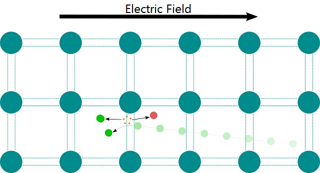
An example of an incoming electron impact ionizing to produce a new electron-hole pair
Therefore, even if the alternating voltage has fallen from the maximum value, a large number of electrons and holes have been generated before, which can continuously generate new electrons and holes through collisions. As a result, the number of electrons and holes will increase constantly when the electric field is larger than the avalanche electric field. And only when the electric field decreases below the avalanche electric field, that is, after the alternating voltage enters the negative half cycle, the avalanche current will begin to decrease.
In this way, the current produced by the avalanche is one-quarter cycle fall behind the alternating voltage in time, or 90 ° lag behind in the phase. After the carriers enter the drift region, the transition process begins. During the transit time, a current appears in the external circuit. As the avalanche current increases, the induced current of the external circuit continues to increase.
Since the holes generated by the avalanche pass through the drift zone at a certain speed, when the avalanche current reaches the maximum value, the induction current does not reach the maximum value. And after the avalanche current decreases from the maximum value, the continuously drifting carriers continue to increase the induced current. When the avalanche current drops to a certain value, the induced current reaches its maximum value and then begins to decrease. Therefore, the induced current lags behind the avalanche current in time.
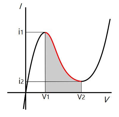
As for a resistor, if an alternating voltage is applied across its two ends, an alternating current will pass through the resistor. The alternating voltage and the alternating current are in the same phase, which means the voltage and the current increase at the same time. When the voltage reaches the maximum value, the current also reaches the maximum value, and when the voltage is zero, the current is also zero.
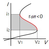
However, for avalanche diodes, the phases of the current and voltage are opposite, and the current-voltage relationship at this time is exactly the opposite of that in the resistor. When the voltage increases, the current decreases. This phenomenon is called "negative resistance", which is a concept to explain the special relationship between current and voltage in a circuit, and does not mean the resistance is “negative”. The current flowing through the resistor consumes energy, and the negative resistance effect can replenish the energy to maintain the resonance circuit for oscillation.
Voltage Controlled Negative Resistance
Current Controlled Negative Resistance
The avalanche diodes can generate large microwave power, but it also has loud noise. They have been widely used as solid microwave power sources in pumping sources for local oscillators and parametric amplifiers.
IV Avalanche Photon Diodes(APD)
Avalanche photon diodes(APD) refer to the photosensitive elements used in laser communications. After a reverse bias is added to the PN junction of a photon diode made of silicon or germanium, the incident light is absorbed by the P-N junction and forms a photocurrent. If we increase the reverse bias, the light current will multiply exponentially, which is called the phenomenon of "avalanche".
1. Working Principle of APD
The avalanche photon diode is a type of optical detection diode with p-n junctions. The avalanche multiplication effect of carriers is used to amplify the photoelectric signal to improve the detection sensitivity. Its basic structure often adopts the Read diode structure (N + PIP +, one side of P + receives light) that is prone to generate avalanche multiplication effect. A large reverse bias can make it reach the avalanche multiplication state. And the light absorption region (P region)is the same as the light multiplication region (I region).

Avalanche Multiplication
When a suitable high reverse bias voltage is applied to the PN junction, the photo-generated carriers in the depletion layer will obtain sufficiently high kinetic energy accelerated by the strong electric field, which will then collide with the lattice and ionize to produce new electron-hole pairs. These carriers will constantly collide and ionize, resulting in the avalanche multiplication of the carriers and obtaining the current gain.
InGaAs (indium gallium arsenide) / InP (indium phosphorus) APD is an ideal photodetector for long-wavelength (1.3 μn, 1.55 μm) optical fiber communication. The optimized structure is shown in the figure. The light-absorbing layer is made of InGaAs material, which has a high absorption coefficient for the light of 1.3 μm and 1.55 μn. In order to avoid the tunnel breakdown of the InGaAs homojunction to occur before the avalanche breakdown, the PN junction is made in the InP window layer to separate the avalanche area from the absorption region. Given that the ionization coefficient of holes in the InP material is larger than that of electrons, n-type InP is used in the avalanche region. And as there is a large valence band barrier in the hetero-interface between n-InP and n-InGaAs, it will easily cause the photo-generated holes to collapse. Therefore, InGaAsP (indium gallium arsenic phosphorus) transition region with the gradually varied band and the gap can be added to form a SAGM (absorption, classification, and multiplication) structure.
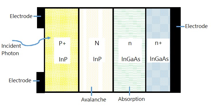
Schematic Model of an InGaAs-InP SAM APD
In APD manufacturing, it is necessary to add a protection ring on the surface of the device to improve the withstand performance for reverse voltage. Si is widely used in APD to detect light below 0.9um, and Ge and InGaAs are commonly used for long-wavelength light above 1um. However, the multiplication of the tunneling current will produce a larger shot noise. Though we could decrease the p-region doping to reduce the tunneling current, this will increase the avalanche voltage. An improved structure called SAM-APD can be adopted. Material with a wide bandgap is used for the doubling region to avoid absorbing light, and a material with a narrow bandgap is applied for the light absorption region. Here, a hetero-junction is used, for which the doping density of the multiplication region can be reduced without affecting the light absorption region to decrease the tunneling current. if it is an abrupt heterojunction, ΔEv will cause the accumulation of photo-generated holes thus affecting the response speed of the device. In this case, a slowly varying layer can be inserted in the middle of the abrupt heterojunction to reduce the effect of ΔEv.
2. Features of Avalanche Photon Diodes
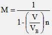
① Avalanche Gain Coefficient(Multiplication Factor)(M)
For the junction with sudden change,
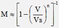
where V is the reverse bias voltage and VB is the avalanche breakdown voltage. N is related to the material, structure, and incident wavelength of the device, which is a constant between 1 to 3.
② Gain Bandwidth Product
When the gain is large and the frequency is high,
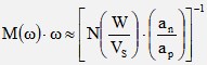
In the equation, ω is the angular frequency, N is a constant, which changes slowly with the ionization coefficient ratio, W is the thickness of the depletion region, Vs is the saturating speed, αn and αp are respectively the ionization coefficients of electrons and holes. The gain-bandwidth product is also constant. To get a high product, an APD with a large Vs, a small W, and a small αn / αp, which means the ionization coefficients of the electrons and holes should have a large difference, and carriers with higher ionization coefficients should be injected into the avalanche area.
③ Excess Noise Factor(F)
During the multiplication process, the noise current increases faster than the signal current.
![]()
where x is called the excess noise index. Avalanche photon diodes with appropriate M value, can gain the best signal-to-noise ratio and make the system reach the highest sensitivity.
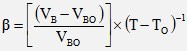
④ Temperature Characteristics
The carrier ionization coefficient decreases with the increase of temperature, which will reduce the multiplication factor increase breakdown voltage. Here, we use the temperature coefficient of the breakdown voltage to describe the temperature characteristics of APD:
 .
.
In this equation, VB and VB0 are breakdown voltages when the temperature is T and T0, respectively.
During the use, the temperature of the working point should be controlled, and an even P-N junction should be manufactured to prevent the breakdown of local junction surfaces.
3. Common Materials of APD
Theoretically, any semiconductor materials can be used in the doubling zone:
● Silicon materials are suitable for visible and near-infrared detection with low multiplication noise (excess noise).
● Germanium (Ge) materials can detect infrared rays with wavelengths no longer than 1.7µ m, but with high multiplication noise.
● InGaAs materials can detect infrared rays with wavelengths exceeding 1.6µ m and the multiplication noise is lower than that of germanium materials. It is generally used in the multiplier region for heterostructure diodes and is also suitable for high-speed(10Gbit/s or higher) optical communication.
● GaN diodes can be applied for ultraviolet detection.
● HgCdTe diodes can detect infrared light with a wavelength up to 14µ m, but need to be cooled to reduce dark current. Very low excess noise can be obtained with this type of diode.
Schematic Illustration of the HgCdTe APD Architecture.
4. Factors Affecting the Avalanche Effect
When a high reverse bias voltage is applied to the diode, the carriers moving in the depletion layer may obtain an avalanche multiplication due to the impact ionization effect. This phenomenon was first discovered in the study of the reverse breakdown mechanism of semiconductor diodes. When the avalanche gain of the carriers reaches very high, the diode enters an avalanche breakdown state. However, in the past, as long as the electric field in the depletion layer was sufficient enough to cause collision ionization, the carriers passing through the depletion layer would have a certain avalanche multiplying value.
The impact ionization effect can also generate the avalanche multiplication of photo-generated carriers so that the semiconductor photon diode has an internal photocurrent gain. In 1953, K.G. McKay and K.B. McCafferty reported the photocurrent multiplication of PN junctions of germanium and silicon as the device approached breakdown. In 1955, S.L.Miller pointed out that in a mutant PN junction, the relation between the multiplication factor M and the reverse bias voltage V can be approximately expressed by the following empirical formula:
where VB is the body breakdown voltage, and n is an index related to the material properties and the types of injected carriers. When the applied bias voltage is very close to the body breakdown voltage, the diode obtains a very high photocurrent gain. The premature breakdown of the PN junction in any small local area will limit the use of the diode, so only when an actual device is highly uniform across the entire PN junction plane, can a high useful average photocurrent gain be obtained. Therefore, from the working state, the avalanche photon diode is a highly uniform semiconductor photon diode that works close to (but has not reached) the avalanche breakdown state.
The average photocurrent gain of APD with good performance can reach tens, hundreds, or even more times The impact ionization capabilities of two kinds of carriers in semiconductors may be different, so the injection of carriers with higher ionization capabilities injected into the depletion region is beneficial to obtain higher avalanche multipliers under the same electric field conditions. However, the avalanche multiplication of photocurrent is not ideal. As the impact ionization of carriers is a random process, the avalanche gain obtained by each carrier in the depletion layer can have a wide probability distribution, so the photocurrent I after multiplication has larger fluctuations than the photocurrent I0 before multiplication, causing additional noise. Compared with the vacuum photomultiplier, this kind of fluctuation is more obvious because both carriers in the semiconductor have ionization ability.
Summary
This time, we've learned about the working principle, oscillation modes, and process of avalanche diodes. Besides, another typical type一 avalanche photon diodes were explained in the final chapter, which includes its working principle and features and influencing factors of the avalanche effect. Hope all of you could have a better understanding of avalanche diodes after reading this article!
Recommended Articles:
 UTMEL
UTMEL
We are the professional distributor of electronic components, providing a large variety of products to save you a lot of time, effort, and cost with our efficient self-customized service. careful order preparation fast delivery service
1.What does an avalanche diode do?
In electronics, an avalanche diode is a diode (made from silicon or other semiconductor) that is designed to experience avalanche breakdown at a specified reverse bias voltage.
2.What is the difference between zener diode and avalanche diode?
The main difference between Zener breakdown and avalanche breakdown is their mechanism of occurrence. Zener breakdown occurs because of the high electric field whereas, the avalanche breakdown occurs because of the collision of free electrons with atoms. Both these breakdowns can occur simultaneously.
3.What is the condition that causes a diode to go into avalanche?
Avalanche occurs in diodes when the voltage across a diode exceeds a specified value. An avalanche diode is a diode that is designed to break down and conduct at a specified reverse bias voltage. This is somewhat similar, but not identical to Zener breakdown.
4.At which voltage avalanche occurs in a diode?
Avalanche breakdown in a diode occurs when we apply high reverse voltage across the diode which is higher than the zener break down voltage. Hence Avalanche breakdown in a diode occurs when reverse bias exceeds a certain value.
5.What is Zener effect and Avalanche effect?
The Zener effect is distinct from avalanche breakdown. The avalanche breakdown occurs in lightly doped junctions, which produce a wider depletion region. Temperature increase in the junction increases the contribution of the Zener effect to breakdown, and decreases the contribution of the avalanche effect.
 All You Need to Know About Rectifier CircuitUTMEL24 April 202517649
All You Need to Know About Rectifier Circuit
Read More 15 Key Elements of Diode SelectionUTMEL26 November 202118921
Hello everyone, I am Rose. Welcome back to the new post today. Diodes are one of the most common components in our circuit boards. So, what factors should be considered when selecting models?
Read More What is a PIN Diode?UTMEL04 February 202110245
While diodes with a simple PN junction are by far the most common type of diode in operation, in a variety of applications, other forms of diode may be used. The PIN diode is one type that is used for a number of circuits. In a variety of places, this diode type is used. For RF switching, the PIN diode is very fine, and the PIN structure in photodiodes is very useful as well.
Read More Microwave Diode: Introduction and TypesUTMEL07 January 202126064
Microwave diodes are diodes that work in the microwave frequency band. It is a solid-state microwave device. Microwave band usually refers to the frequency from 300 MHz to 3000 GHz. After the discovery of the point contact diode effect at the end of the 19th century, microwave diodes such as PIN diodes, varactor diodes, and Schottky diode tubes appeared one after another. Microwave diodes have the advantages of small size and high reliability, and are used in microwave oscillation, amplification, frequency conversion, switching, phase shifting and modulation.
Read More What Determines the Maximum Operating Frequency of a Diode?UTMEL29 June 202212945
Hello, wish you a wonderful day. In this essay, we first pose the following query: what determines the diode's maximum operating frequency? In regards to the solution, the first thing we need to understand is that the junction capacitance and the reverse recovery time of the diode are two distinct concepts. The charging and discharging times of the junction capacitance cannot match the reverse recovery time. You say that, why? Let's start by taking a look at these facts.
Read More
Subscribe to Utmel !
![BLM41PG102SH1L]() BLM41PG102SH1L
BLM41PG102SH1LMurata Electronics
![FBMH1608HM102-T]() FBMH1608HM102-T
FBMH1608HM102-TTaiyo Yuden
![BLM18BA121SN1D]() BLM18BA121SN1D
BLM18BA121SN1DMurata Electronics
![742792034]() 742792034
742792034Würth Elektronik
![FBMH1608HM101-T]() FBMH1608HM101-T
FBMH1608HM101-TTaiyo Yuden
![MH2029-221Y]() MH2029-221Y
MH2029-221YBourns Inc.
![ACF321825-102-TD01]() ACF321825-102-TD01
ACF321825-102-TD01TDK Corporation
![NFM18PC225B0J3D]() NFM18PC225B0J3D
NFM18PC225B0J3DMurata Electronics
![BK1005LM182-T]() BK1005LM182-T
BK1005LM182-TTaiyo Yuden
![742792096]() 742792096
742792096Würth Elektronik


