
 Product
 Brand
Brand Articles
 Tools
Tools
Analog Devices AD8032 Selection Guide for Your Projects

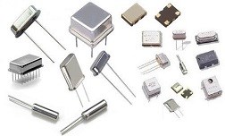
2 Channels 15mA per Channel 450nA 90 dB Instrumentational OP Amps 5V 2.7V~12V ±1.35V~6V AD8032 8 Pins 8-TSSOP, 8-MSOP (0.118, 3.00mm Width)


2 Channels 15mA per Channel 450nA 90 dB Instrumentational OP Amps 5V 2.7V~12V ±1.35V~6V AD8032 8 Pins 8-TSSOP, 8-MSOP (0.118, 3.00mm Width)
Choose the right AD8032 variant for your 2025 project by evaluating performance metrics, environmental factors, and compatibility for optimal results.
Product Introduction
Choosing the right AD8032 variant can make or break your project. Each variant offers unique features, and selecting the wrong one may lead to performance issues or inefficiencies. You must align your choice with your project's specific needs to ensure success. This guide simplifies the selection process, helping you confidently navigate the options and make an informed decision.
Pro tip: A well-matched AD8032 variant not only enhances performance but also saves time and resources.
Define Your Project Requirements
When selecting the right AD8032 variant, understanding your project requirements is the first and most critical step. This ensures that the chosen component aligns perfectly with your goals and delivers optimal performance.
Identify Key Performance Metrics
Start by identifying the key performance metrics your project demands. These metrics often include bandwidth, slew rate, power consumption, and noise levels. For example, if your project involves high-speed signal processing, you’ll need an AD8032 variant with a high slew rate and wide bandwidth. On the other hand, low-power applications may prioritize energy efficiency over speed.
Recent research highlights the growing importance of energy-efficient semiconductor designs. Innovations in advanced chip packaging have become essential for meeting the performance needs of modern electronic projects. These advancements not only enhance performance but also reduce production costs and energy consumption. With data centers projected to consume nearly 1,000 TWh of electricity globally by 2030, selecting components like the AD8032 that support efficient designs is more important than ever.
Tip: Create a checklist of your project’s performance requirements. This will help you compare AD8032 variants more effectively.
Consider Environmental Factors
Environmental conditions can significantly impact the performance of your AD8032. Factors such as temperature range, humidity, and electromagnetic interference (EMI) should guide your selection. For instance, if your project operates in extreme temperatures, choose an AD8032 variant with a wide operating temperature range. Similarly, environments with high EMI may require additional shielding or a variant with better noise immunity.
Think about where and how your project will function. Will it be used outdoors, in industrial settings, or within a controlled lab environment? Each scenario presents unique challenges. By accounting for these factors early, you can avoid costly redesigns or performance issues later.
Note: Always consult the datasheet for detailed environmental specifications of each AD8032 variant.
Understand AD8032 Variants
Overview of Available Variants
The AD8032 family includes several variants, each designed to meet specific application needs. These variants differ in performance characteristics, making it essential to understand their unique features before making a choice. By doing so, you can ensure that the selected variant aligns with your project requirements.
Here are some of the key variants available:
Standard AD8032: This variant offers a balance between speed and power consumption, making it suitable for general-purpose applications.
Low-Power AD8032: Designed for energy-efficient systems, this variant minimizes power usage without compromising essential performance metrics.
High-Speed AD8032: Ideal for high-frequency applications, this variant provides a higher slew rate and wider bandwidth.
Extended Temperature Range AD8032: Built for harsh environments, this variant operates reliably across a broader temperature range.
Tip: Always check the datasheet for each variant to understand its specific capabilities and limitations.
Compare Specifications
Comparing the specifications of AD8032 variants helps you identify the best match for your project. Focus on the parameters that matter most to your application. Below is a table summarizing some key specifications of the common AD8032 variants:
| Variant | Bandwidth (MHz) | Slew Rate (V/µs) | Power Consumption (mW) | Operating Temperature (°C) |
|---|---|---|---|---|
| Standard AD8032 | 80 | 30 | 5.5 | -40 to 85 |
| Low-Power AD8032 | 60 | 20 | 3.0 | -40 to 85 |
| High-Speed AD8032 | 120 | 50 | 7.0 | -40 to 85 |
| Extended Temperature AD8032 | 80 | 30 | 5.5 | -55 to 125 |
When comparing these specifications, consider how each parameter impacts your project. For instance, if your design requires rapid signal transitions, prioritize a variant with a higher slew rate. If energy efficiency is critical, focus on power consumption.
Note: The operating temperature range is crucial for projects in extreme environments. Always verify that the selected variant meets your environmental requirements.
By carefully analyzing these specifications, you can confidently choose the AD8032 variant that best suits your needs.
Evaluate Compatibility
Circuit Design Considerations
When integrating the AD8032 into your circuit, you must evaluate its compatibility with your design. Start by reviewing the input and output impedance requirements of your circuit. The AD8032 operates optimally when paired with components that match its impedance characteristics. Mismatched impedance can lead to signal distortion or reduced performance.
You should also consider the feedback network. The AD8032 supports various configurations, including inverting and non-inverting setups. Each configuration affects gain, stability, and bandwidth differently. For example, a non-inverting configuration provides higher input impedance, which may benefit sensor-based applications. Always simulate your circuit design using tools like SPICE to verify stability and performance before finalizing the layout.
Tip: Keep trace lengths short and use proper grounding techniques to minimize noise and interference in your circuit.
Power Supply and Pin Configuration
The AD8032 offers flexibility in power supply configurations, making it suitable for single-supply or dual-supply systems. This versatility allows you to adapt the component to your project's specific power requirements. For instance, the CN0277 reference design demonstrates how the AD8032 can operate effectively in various configurations. Below is a table summarizing compatibility with other components:
| Component | Description |
|---|---|
| AD8032 | Can be used in various power supply configurations as per CN0277 reference design. |
| ADA4897-1 | Can be replaced with ADA4897-2, indicating compatibility with dual versions. |
Pin configuration is another critical factor. The AD8032 features a standard pinout, simplifying integration into existing designs. Ensure that your PCB layout aligns with the pin assignments to avoid connection errors. Double-check the datasheet for details on pin functions, such as power supply pins, input/output pins, and ground connections.
Note: Proper decoupling capacitors near the power supply pins can improve stability and reduce noise.
Test and Validate
Testing and validation ensure that your chosen AD8032 variant performs as expected in your project. This step helps you identify potential issues early and refine your design for optimal results.
Prototype Testing
Building a prototype is the first step in testing. Assemble your circuit with the selected AD8032 variant and verify that all connections match your design. Use a breadboard or PCB to create a functional model. This allows you to test the component in a controlled environment before finalizing your design.
During testing, focus on key performance metrics like signal integrity, gain, and stability. Use an oscilloscope to observe the output waveform and confirm that it meets your expectations. If you notice any discrepancies, adjust the circuit parameters or consider alternative configurations. For example, tweaking the feedback resistor values can improve gain accuracy.
Tip: Document your observations during testing. This will help you track changes and identify what works best for your application.
Performance Validation
After prototype testing, validate the AD8032's performance under real-world conditions. Simulate the actual operating environment of your project. For instance, if your design will function in high-temperature settings, test the circuit at elevated temperatures to ensure reliability.
Measure parameters like bandwidth, noise levels, and power consumption. Compare these results with the specifications in the datasheet to confirm that the component meets your requirements. If your project involves high-speed signals, pay close attention to the slew rate and ensure it aligns with your design goals.
Note: Use tools like the Analog Filter Wizard to fine-tune your design and achieve optimal performance.
Testing and validation provide confidence in your design. By addressing potential issues early, you can avoid costly revisions and ensure your project succeeds.
Selecting the right AD8032 variant involves four key steps: defining your project requirements, understanding the available variants, evaluating compatibility, and testing your design. Each step ensures that the component aligns with your specific goals and delivers optimal performance.
Reminder: Always consult the datasheet for detailed specifications. Tools like the Analog Filter Wizard can simplify design adjustments and improve results.
By following this guide, you can confidently choose the best AD8032 variant for your 2025 projects, ensuring efficiency and success.
FAQ
What makes the AD8032 suitable for high-speed applications?
The AD8032 offers a high slew rate and wide bandwidth, making it ideal for rapid signal transitions. These features ensure accurate signal reproduction in high-frequency designs, such as communication systems or video processing.
How do I choose the right AD8032 variant for my project?
Focus on your project’s key requirements, like bandwidth, power consumption, and operating temperature. Use a checklist to compare specifications across variants. Always consult the datasheet for detailed insights.
Can I use the AD8032 in low-power designs?
Yes, the Low-Power AD8032 variant is optimized for energy-efficient applications. It minimizes power consumption while maintaining essential performance metrics, making it perfect for battery-operated devices.
What tools can help me design with the AD8032?
You can use tools like SPICE for circuit simulation and the Analog Filter Wizard for filter design. These tools simplify testing and ensure your design meets performance goals.
Does the AD8032 work in extreme environments?
The Extended Temperature Range AD8032 variant operates reliably between -55°C and 125°C. This makes it suitable for industrial or outdoor applications where temperature extremes are common.
Tip: Always test your design under real-world conditions to ensure reliability.
Specifications
- TypeParameter
- Lifecycle Status
Lifecycle Status refers to the current stage of an electronic component in its product life cycle, indicating whether it is active, obsolete, or transitioning between these states. An active status means the component is in production and available for purchase. An obsolete status indicates that the component is no longer being manufactured or supported, and manufacturers typically provide a limited time frame for support. Understanding the lifecycle status is crucial for design engineers to ensure continuity and reliability in their projects.
PRODUCTION (Last Updated: 1 week ago) - Factory Lead Time8 Weeks
- Contact Plating
Contact plating (finish) provides corrosion protection for base metals and optimizes the mechanical and electrical properties of the contact interfaces.
Tin - Mounting Type
The "Mounting Type" in electronic components refers to the method used to attach or connect a component to a circuit board or other substrate, such as through-hole, surface-mount, or panel mount.
Surface Mount - Package / Case
refers to the protective housing that encases an electronic component, providing mechanical support, electrical connections, and thermal management.
8-TSSOP, 8-MSOP (0.118, 3.00mm Width) - Surface Mount
having leads that are designed to be soldered on the side of a circuit board that the body of the component is mounted on.
YES - Number of Pins8
- Operating Temperature
The operating temperature is the range of ambient temperature within which a power supply, or any other electrical equipment, operate in. This ranges from a minimum operating temperature, to a peak or maximum operating temperature, outside which, the power supply may fail.
-40°C~85°C - Packaging
Semiconductor package is a carrier / shell used to contain and cover one or more semiconductor components or integrated circuits. The material of the shell can be metal, plastic, glass or ceramic.
Tube - JESD-609 Code
The "JESD-609 Code" in electronic components refers to a standardized marking code that indicates the lead-free solder composition and finish of electronic components for compliance with environmental regulations.
e3 - Pbfree Code
The "Pbfree Code" parameter in electronic components refers to the code or marking used to indicate that the component is lead-free. Lead (Pb) is a toxic substance that has been widely used in electronic components for many years, but due to environmental concerns, there has been a shift towards lead-free alternatives. The Pbfree Code helps manufacturers and users easily identify components that do not contain lead, ensuring compliance with regulations and promoting environmentally friendly practices. It is important to pay attention to the Pbfree Code when selecting electronic components to ensure they meet the necessary requirements for lead-free applications.
no - Part Status
Parts can have many statuses as they progress through the configuration, analysis, review, and approval stages.
Active - Moisture Sensitivity Level (MSL)
Moisture Sensitivity Level (MSL) is a standardized rating that indicates the susceptibility of electronic components, particularly semiconductors, to moisture-induced damage during storage and the soldering process, defining the allowable exposure time to ambient conditions before they require special handling or baking to prevent failures
1 (Unlimited) - Number of Terminations8
- ECCN Code
An ECCN (Export Control Classification Number) is an alphanumeric code used by the U.S. Bureau of Industry and Security to identify and categorize electronic components and other dual-use items that may require an export license based on their technical characteristics and potential for military use.
EAR99 - Max Power Dissipation
The maximum power that the MOSFET can dissipate continuously under the specified thermal conditions.
600mW - Terminal Position
In electronic components, the term "Terminal Position" refers to the physical location of the connection points on the component where external electrical connections can be made. These connection points, known as terminals, are typically used to attach wires, leads, or other components to the main body of the electronic component. The terminal position is important for ensuring proper connectivity and functionality of the component within a circuit. It is often specified in technical datasheets or component specifications to help designers and engineers understand how to properly integrate the component into their circuit designs.
DUAL - Terminal Form
Occurring at or forming the end of a series, succession, or the like; closing; concluding.
GULL WING - Peak Reflow Temperature (Cel)
Peak Reflow Temperature (Cel) is a parameter that specifies the maximum temperature at which an electronic component can be exposed during the reflow soldering process. Reflow soldering is a common method used to attach electronic components to a circuit board. The Peak Reflow Temperature is crucial because it ensures that the component is not damaged or degraded during the soldering process. Exceeding the specified Peak Reflow Temperature can lead to issues such as component failure, reduced performance, or even permanent damage to the component. It is important for manufacturers and assemblers to adhere to the recommended Peak Reflow Temperature to ensure the reliability and functionality of the electronic components.
260 - Number of Functions2
- Supply Voltage
Supply voltage refers to the electrical potential difference provided to an electronic component or circuit. It is crucial for the proper operation of devices, as it powers their functions and determines performance characteristics. The supply voltage must be within specified limits to ensure reliability and prevent damage to components. Different electronic devices have specific supply voltage requirements, which can vary widely depending on their design and intended application.
5V - Terminal Pitch
The center distance from one pole to the next.
0.65mm - Time@Peak Reflow Temperature-Max (s)
Time@Peak Reflow Temperature-Max (s) refers to the maximum duration that an electronic component can be exposed to the peak reflow temperature during the soldering process, which is crucial for ensuring reliable solder joint formation without damaging the component.
30 - Base Part Number
The "Base Part Number" (BPN) in electronic components serves a similar purpose to the "Base Product Number." It refers to the primary identifier for a component that captures the essential characteristics shared by a group of similar components. The BPN provides a fundamental way to reference a family or series of components without specifying all the variations and specific details.
AD8032 - Pin Count
a count of all of the component leads (or pins)
8 - Output Type
The "Output Type" parameter in electronic components refers to the type of signal or data that is produced by the component as an output. This parameter specifies the nature of the output signal, such as analog or digital, and can also include details about the voltage levels, current levels, frequency, and other characteristics of the output signal. Understanding the output type of a component is crucial for ensuring compatibility with other components in a circuit or system, as well as for determining how the output signal can be utilized or processed further. In summary, the output type parameter provides essential information about the nature of the signal that is generated by the electronic component as its output.
Rail-to-Rail - Operating Supply Voltage
The voltage level by which an electrical system is designated and to which certain operating characteristics of the system are related.
5V - Number of Channels2
- Operating Supply Current
Operating Supply Current, also known as supply current or quiescent current, is a crucial parameter in electronic components that indicates the amount of current required for the device to operate under normal conditions. It represents the current drawn by the component from the power supply while it is functioning. This parameter is important for determining the power consumption of the component and is typically specified in datasheets to help designers calculate the overall power requirements of their circuits. Understanding the operating supply current is essential for ensuring proper functionality and efficiency of electronic systems.
3.2mA - Nominal Supply Current
Nominal current is the same as the rated current. It is the current drawn by the motor while delivering rated mechanical output at its shaft.
3.2mA - Power Dissipation
the process by which an electronic or electrical device produces heat (energy loss or waste) as an undesirable derivative of its primary action.
600mW - Output Current
The rated output current is the maximum load current that a power supply can provide at a specified ambient temperature. A power supply can never provide more current that it's rated output current unless there is a fault, such as short circuit at the load.
15mA - Quiescent Current
The quiescent current is defined as the current level in the amplifier when it is producing an output of zero.
900μA - Slew Rate
the maximum rate of output voltage change per unit time.
35V/μs - Amplifier Type
Amplifier Type refers to the classification or categorization of amplifiers based on their design, functionality, and characteristics. Amplifiers are electronic devices that increase the amplitude of a signal, such as voltage or current. The type of amplifier determines its specific application, performance capabilities, and operating characteristics. Common types of amplifiers include operational amplifiers (op-amps), power amplifiers, audio amplifiers, and radio frequency (RF) amplifiers. Understanding the amplifier type is crucial for selecting the right component for a particular circuit or system design.
Voltage Feedback - Common Mode Rejection Ratio
Common Mode Rejection Ratio (CMRR) is a measure of the ability of a differential amplifier to reject input signals that are common to both input terminals. It is defined as the ratio of the differential gain to the common mode gain. A high CMRR indicates that the amplifier can effectively eliminate noise and interference that affects both inputs simultaneously, enhancing the fidelity of the amplified signal. CMRR is typically expressed in decibels (dB), with higher values representing better performance in rejecting common mode signals.
90 dB - Current - Input Bias
The parameter "Current - Input Bias" in electronic components refers to the amount of current required at the input terminal of a device to maintain proper operation. It is a crucial specification as it determines the minimum input current needed for the component to function correctly. Input bias current can affect the performance and accuracy of the device, especially in precision applications where small signal levels are involved. It is typically specified in datasheets for operational amplifiers, transistors, and other semiconductor devices to provide users with important information for circuit design and analysis.
450nA - Voltage - Supply, Single/Dual (±)
The parameter "Voltage - Supply, Single/Dual (±)" in electronic components refers to the power supply voltage required for the proper operation of the component. This parameter indicates whether the component requires a single power supply voltage (e.g., 5V) or a dual power supply voltage (e.g., ±15V). For components that require a single power supply voltage, only one voltage level is needed for operation. On the other hand, components that require a dual power supply voltage need both positive and negative voltage levels to function correctly.Understanding the voltage supply requirements of electronic components is crucial for designing and integrating them into circuits to ensure proper functionality and prevent damage due to incorrect voltage levels.
2.7V~12V ±1.35V~6V - Output Current per Channel
Output Current per Channel is a specification commonly found in electronic components such as amplifiers, audio interfaces, and power supplies. It refers to the maximum amount of electrical current that can be delivered by each individual output channel of the component. This parameter is important because it determines the capacity of the component to drive connected devices or loads. A higher output current per channel means the component can deliver more power to connected devices, while a lower output current may limit the performance or functionality of the component in certain applications. It is crucial to consider the output current per channel when selecting electronic components to ensure they can meet the power requirements of the intended system or setup.
15mA - Input Offset Voltage (Vos)
Input Offset Voltage (Vos) is a key parameter in electronic components, particularly in operational amplifiers. It refers to the voltage difference that must be applied between the two input terminals of the amplifier to nullify the output voltage when the input terminals are shorted together. In simpler terms, it represents the voltage required to bring the output of the amplifier to zero when there is no input signal present. Vos is an important parameter as it can introduce errors in the output signal of the amplifier, especially in precision applications where accuracy is crucial. Minimizing Vos is essential to ensure the amplifier operates with high precision and accuracy.
1.5mV - Gain Bandwidth Product
The gain–bandwidth product (designated as GBWP, GBW, GBP, or GB) for an amplifier is the product of the amplifier's bandwidth and the gain at which the bandwidth is measured.
40MHz - Neg Supply Voltage-Nom (Vsup)
The parameter "Neg Supply Voltage-Nom (Vsup)" in electronic components refers to the nominal negative supply voltage that the component requires to operate within its specified performance characteristics. This parameter indicates the minimum voltage level that must be provided to the component's negative supply pin for proper functionality. It is important to ensure that the negative supply voltage provided to the component does not exceed the maximum specified value to prevent damage or malfunction. Understanding and adhering to the specified negative supply voltage requirements is crucial for the reliable operation of the electronic component in a circuit.
-5V - Unity Gain BW-Nom
Unity Gain Bandwidth, often abbreviated as Unity Gain BW or UGBW, refers to the frequency at which an amplifier can provide a gain of one (0 dB). It is a critical parameter in assessing the performance of operational amplifiers and other amplifying devices, indicating the range of frequencies over which the amplifier can operate without distortion. Unity Gain BW is particularly important in applications where signal fidelity is crucial, as it helps determine the maximum frequency of operation for a given gain level. As the gain is reduced, the bandwidth typically increases, ensuring that the amplifier can still operate effectively across various signal frequencies.
80000 kHz - Voltage Gain
Voltage gain is a measure of how much an electronic component or circuit amplifies an input voltage signal to produce an output voltage signal. It is typically expressed as a ratio or in decibels (dB). A higher voltage gain indicates a greater amplification of the input signal. Voltage gain is an important parameter in amplifiers, where it determines the level of amplification provided by the circuit. It is calculated by dividing the output voltage by the input voltage and is a key factor in determining the overall performance and functionality of electronic devices.
82dB - Power Supply Rejection Ratio (PSRR)
Power Supply Rejection Ratio (PSRR) is a measure of how well an electronic component, such as an operational amplifier or voltage regulator, can reject changes in its supply voltage. It indicates the ability of the component to maintain a stable output voltage despite fluctuations in the input supply voltage. A higher PSRR value signifies better performance in rejecting noise and variations from the power supply, leading to improved signal integrity and more reliable operation in electronic circuits. PSRR is typically expressed in decibels (dB).
86dB - Low-Offset
Low-offset is a parameter used to describe the level of offset voltage in electronic components, particularly in operational amplifiers. Offset voltage refers to the small voltage difference that exists between the input terminals of the amplifier when the input voltage is zero. A low-offset value indicates that this voltage difference is minimal, which is desirable for accurate signal processing and amplification. Components with low-offset specifications are preferred in applications where precision and accuracy are critical, such as in instrumentation and measurement systems. Minimizing offset voltage helps reduce errors and ensures the faithful reproduction of input signals by the amplifier.
NO - Frequency Compensation
Frequency compensation is implemented by modifying the gain and phase characteristics of the amplifier's open loop output or of its feedback network, or both, in such a way as to avoid the conditions leading to oscillation. This is usually done by the internal or external use of resistance-capacitance networks.
YES - Supply Voltage Limit-Max
The parameter "Supply Voltage Limit-Max" in electronic components refers to the maximum voltage that the component can safely handle without getting damaged. This specification is crucial for ensuring the reliable operation and longevity of the component within a given electrical system. Exceeding the maximum supply voltage limit can lead to overheating, electrical breakdown, or permanent damage to the component. It is important to carefully adhere to this limit when designing and operating electronic circuits to prevent potential failures and ensure the overall system's performance and safety.
6.3V - Voltage - Input Offset
Voltage - Input Offset is a parameter that refers to the difference in voltage between the input terminals of an electronic component, such as an operational amplifier, when the input voltage is zero. It is an important characteristic that can affect the accuracy and performance of the component in various applications. A low input offset voltage is desirable as it indicates that the component will have minimal error in its output when the input signal is near zero. Manufacturers typically provide this specification in the component's datasheet to help users understand the component's behavior and make informed decisions when designing circuits.
1mV - Settling Time
In control theory the settling time of a dynamical system such as an amplifier or other output device is the time elapsed from the application of an ideal instantaneous step input to the time at which the amplifier output has entered and remained within a specified error band.
125 ns - Low-Bias
Low-bias in electronic components refers to a design or configuration that minimizes the amount of bias current flowing through the component. Bias current is a small, steady current that is used to establish the operating point of a component, such as a transistor or amplifier. By reducing the bias current to a low level, the component can operate with lower power consumption and potentially lower distortion. Low-bias components are often used in applications where power efficiency and signal fidelity are important, such as in audio amplifiers or battery-powered devices. Overall, the low-bias parameter indicates the ability of the component to operate efficiently and accurately with minimal bias current.
NO - Micropower
the use of very small electric generators and prime movers or devices to convert heat or motion to electricity, for use close to the generator.
NO - Programmable Power
A programmable power supply provides remote control capability of the output voltage(s) via an analog control signal controlled by keypad or rotary switch from the front panel of the power supply or via a computer interface such as RS232, GPIB, or USB.
NO - Dual Supply Voltage
Dual Supply Voltage refers to an electronic component's requirement for two separate power supply voltages, typically one positive and one negative. This configuration is commonly used in operational amplifiers, analog circuits, and certain digital devices to allow for greater signal handling capabilities and improved performance. The use of dual supply voltages enables the device to process bipolar signals, thereby enhancing its functionality in various applications.
5V - Input Capacitance
The capacitance between the input terminals of an op amp with either input grounded. It is expressed in units of farads.
1.6pF - Height850μm
- Length3mm
- Width3mm
- REACH SVHC
The parameter "REACH SVHC" in electronic components refers to the compliance with the Registration, Evaluation, Authorization, and Restriction of Chemicals (REACH) regulation regarding Substances of Very High Concern (SVHC). SVHCs are substances that may have serious effects on human health or the environment, and their use is regulated under REACH to ensure their safe handling and minimize their impact.Manufacturers of electronic components need to declare if their products contain any SVHCs above a certain threshold concentration and provide information on the safe use of these substances. This information allows customers to make informed decisions about the potential risks associated with using the components and take appropriate measures to mitigate any hazards.Ensuring compliance with REACH SVHC requirements is essential for electronics manufacturers to meet regulatory standards, protect human health and the environment, and maintain transparency in their supply chain. It also demonstrates a commitment to sustainability and responsible manufacturing practices in the electronics industry.
No SVHC - Radiation Hardening
Radiation hardening is the process of making electronic components and circuits resistant to damage or malfunction caused by high levels of ionizing radiation, especially for environments in outer space (especially beyond the low Earth orbit), around nuclear reactors and particle accelerators, or during nuclear accidents or nuclear warfare.
No - RoHS Status
RoHS means “Restriction of Certain Hazardous Substances” in the “Hazardous Substances Directive” in electrical and electronic equipment.
ROHS3 Compliant - Lead Free
Lead Free is a term used to describe electronic components that do not contain lead as part of their composition. Lead is a toxic material that can have harmful effects on human health and the environment, so the electronics industry has been moving towards lead-free components to reduce these risks. Lead-free components are typically made using alternative materials such as silver, copper, and tin. Manufacturers must comply with regulations such as the Restriction of Hazardous Substances (RoHS) directive to ensure that their products are lead-free and environmentally friendly.
Contains Lead
Parts with Similar Specs
- ImagePart NumberManufacturerPackage / CaseNumber of PinsSlew RateGain Bandwidth ProductInput Offset Voltage (Vos)Power Supply Rejection Ratio (PSRR)Common Mode Rejection RatioSupply VoltageView Compare
![AD8032ARMZ]()
AD8032ARMZ
8-TSSOP, 8-MSOP (0.118, 3.00mm Width)
8
35V/μs
40 MHz
1.5 mV
86 dB
90 dB
5 V
![AD8652ARMZ-REEL]()
8-TSSOP, 8-MSOP (0.118, 3.00mm Width)
8
41V/μs
50MHz
350 μV
94 dB
95 dB
5 V
![LTC6244HMS8#PBF]()
8-TSSOP, 8-MSOP (0.118, 3.00mm Width)
8
41V/μs
-
350 μV
94 dB
95 dB
5 V
![AD8652ARMZ]()
8-TSSOP, 8-MSOP (0.118, 3.00mm Width)
8
35V/μs
-
150 μV
85 dB
85 dB
2.5 V
![LMP7718MM/NOPB]()
MSOP
8
40 V/μs
30 MHz
40 μV
75 dB
74 dB
-


Datasheet PDF
- Datasheets :
AD8032ARMZ-Analog-Devices-datasheet-23752812.pdf
AD8032ARMZ-Analog-Devices-datasheet-5318383.pdf
AD8032ARMZ-Analog-Devices-datasheet-14139335.pdf
AD8032ARMZ-Analog-Devices-datasheet-16753.pdf
AD8032ARMZ-Analog-Devices-datasheet-9990395.pdf
pid_7888196_ad8032armz-analog-devices-datasheet-23752812.pdf
- PCN Assembly/Origin :
- ConflictMineralStatement :
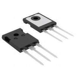 IRFP260 Power MOSFET: 46A 200V N-Channel TO247, IRFP260 Equivalents and Datasheet
29 December 20214448
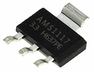 AMS1117 1A Low Dropout Voltage Regulator: Datasheet, 3.3 V Regulators and Pinout
23 November 202128874
 ADAU1701: Detailed Datasheet, Pinout, and Alternatives Guide
26 January 20261397
![PC817 Optoisolators Transistor Photovoltaic 4DIP[Video]: Pinout, Datasheet, and Equivalents](https://res.utmel.com/Images/Article/c21d5d4a-7f97-47d9-a2df-3305ccf27127.jpg) PC817 Optoisolators Transistor Photovoltaic 4DIP[Video]: Pinout, Datasheet, and Equivalents
PC817 Optoisolators Transistor Photovoltaic 4DIP[Video]: Pinout, Datasheet, and Equivalents24 March 20224328
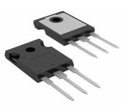 IRFP250N N-Channel MOSFET: IRFP250N Power MOSFET, Datasheet pdf and Equivalents
27 December 202114690
 PIC16F505 8-Bit Flash Microcontroller: Datasheet, Pinout, Feature
27 December 20213808
 1N4001 Diodes: Pinout, Datasheet and Alternatives
06 July 202110537
![Difference Between BS170 N-Channel MOSFET vs. 2N7000 N-Channel MOSFET [Video&FAQ]](https://res.utmel.com/Images/Article/991b840d-d62d-4cd0-b756-4ec2fa6e357e.jpg) Difference Between BS170 N-Channel MOSFET vs. 2N7000 N-Channel MOSFET [Video&FAQ]
Difference Between BS170 N-Channel MOSFET vs. 2N7000 N-Channel MOSFET [Video&FAQ]11 April 202211133
 Introduction to BAW Filter
25 September 202111736
 Detailed Analysis of Analog IC
22 November 20213629
 A Simple Method to Build a Programmable Oscillator
27 May 20227169
 What are Fiber Optic Patch Cables?
11 February 20228144
 What is a Cascode Amplifier?
27 March 202515271
 Getting Started with Arduino: What is Arduino and How to Use Arduino Boards
28 September 20236684
 Comprehensive Analysis of Each Functional Circuit of Switching Power Supply
06 May 20225552
 Discovering New and Advanced Methodology for Determining the Dynamic Characterization of Wide Bandgap Devices
15 March 20242511
Analog Devices Inc.
In Stock: 58
United States
China
Canada
Japan
Russia
Germany
United Kingdom
Singapore
Italy
Hong Kong(China)
Taiwan(China)
France
Korea
Mexico
Netherlands
Malaysia
Austria
Spain
Switzerland
Poland
Thailand
Vietnam
India
United Arab Emirates
Afghanistan
Åland Islands
Albania
Algeria
American Samoa
Andorra
Angola
Anguilla
Antigua & Barbuda
Argentina
Armenia
Aruba
Australia
Azerbaijan
Bahamas
Bahrain
Bangladesh
Barbados
Belarus
Belgium
Belize
Benin
Bermuda
Bhutan
Bolivia
Bonaire, Sint Eustatius and Saba
Bosnia & Herzegovina
Botswana
Brazil
British Indian Ocean Territory
British Virgin Islands
Brunei
Bulgaria
Burkina Faso
Burundi
Cabo Verde
Cambodia
Cameroon
Cayman Islands
Central African Republic
Chad
Chile
Christmas Island
Cocos (Keeling) Islands
Colombia
Comoros
Congo
Congo (DRC)
Cook Islands
Costa Rica
Côte d’Ivoire
Croatia
Cuba
Curaçao
Cyprus
Czechia
Denmark
Djibouti
Dominica
Dominican Republic
Ecuador
Egypt
El Salvador
Equatorial Guinea
Eritrea
Estonia
Eswatini
Ethiopia
Falkland Islands
Faroe Islands
Fiji
Finland
French Guiana
French Polynesia
Gabon
Gambia
Georgia
Ghana
Gibraltar
Greece
Greenland
Grenada
Guadeloupe
Guam
Guatemala
Guernsey
Guinea
Guinea-Bissau
Guyana
Haiti
Honduras
Hungary
Iceland
Indonesia
Iran
Iraq
Ireland
Isle of Man
Israel
Jamaica
Jersey
Jordan
Kazakhstan
Kenya
Kiribati
Kosovo
Kuwait
Kyrgyzstan
Laos
Latvia
Lebanon
Lesotho
Liberia
Libya
Liechtenstein
Lithuania
Luxembourg
Macao(China)
Madagascar
Malawi
Maldives
Mali
Malta
Marshall Islands
Martinique
Mauritania
Mauritius
Mayotte
Micronesia
Moldova
Monaco
Mongolia
Montenegro
Montserrat
Morocco
Mozambique
Myanmar
Namibia
Nauru
Nepal
New Caledonia
New Zealand
Nicaragua
Niger
Nigeria
Niue
Norfolk Island
North Korea
North Macedonia
Northern Mariana Islands
Norway
Oman
Pakistan
Palau
Palestinian Authority
Panama
Papua New Guinea
Paraguay
Peru
Philippines
Pitcairn Islands
Portugal
Puerto Rico
Qatar
Réunion
Romania
Rwanda
Samoa
San Marino
São Tomé & Príncipe
Saudi Arabia
Senegal
Serbia
Seychelles
Sierra Leone
Sint Maarten
Slovakia
Slovenia
Solomon Islands
Somalia
South Africa
South Sudan
Sri Lanka
St Helena, Ascension, Tristan da Cunha
St. Barthélemy
St. Kitts & Nevis
St. Lucia
St. Martin
St. Pierre & Miquelon
St. Vincent & Grenadines
Sudan
Suriname
Svalbard & Jan Mayen
Sweden
Syria
Tajikistan
Tanzania
Timor-Leste
Togo
Tokelau
Tonga
Trinidad & Tobago
Tunisia
Turkey
Turkmenistan
Turks & Caicos Islands
Tuvalu
U.S. Outlying Islands
U.S. Virgin Islands
Uganda
Ukraine
Uruguay
Uzbekistan
Vanuatu
Vatican City
Venezuela
Wallis & Futuna
Yemen
Zambia
Zimbabwe
![AD826AR-REEL7]() AD826AR-REEL7
AD826AR-REEL7Analog Devices Inc.
![AD8062ARM]() AD8062ARM
AD8062ARMAnalog Devices Inc.
![AD8532ARU-REEL]() AD8532ARU-REEL
AD8532ARU-REELAnalog Devices Inc.
![OP113ES]() OP113ES
OP113ESAnalog Devices Inc.
![SSM2142P]() SSM2142P
SSM2142PAnalog Devices, Inc.
![LTC1050CS8]() LTC1050CS8
LTC1050CS8Linear Technology/Analog Devices
![AMP02EPZ]() AMP02EPZ
AMP02EPZAnalog Devices Inc.
![AD822ARZ-REEL7]() AD822ARZ-REEL7
AD822ARZ-REEL7Analog Devices Inc.
![OP2177ARZ-REEL7]() OP2177ARZ-REEL7
OP2177ARZ-REEL7Analog Devices Inc.
![AD8066ARZ-R7]() AD8066ARZ-R7
AD8066ARZ-R7Analog Devices Inc.


