
 Product
 Brand
Brand Articles
 Tools
Tools
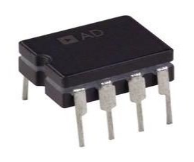
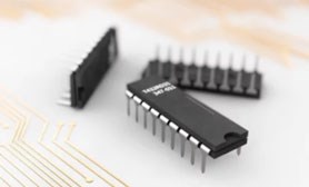
AD8226 Instrumentation Amplifier: Rail-to-Rail Output, 8SOIC AD8226 Pinout and Datasheet

1 Channels 13mA per Channel 20nA 105 dB Instrumentational OP Amps 0.027μA 2.2V~36V ±1.35V~18V AD8226 8 Pins 8-SOIC (0.154, 3.90mm Width)


1 Channels 13mA per Channel 20nA 105 dB Instrumentational OP Amps 0.027μA 2.2V~36V ±1.35V~18V AD8226 8 Pins 8-SOIC (0.154, 3.90mm Width)
The AD8226 is a low-cost, wide-supply range instrumentation amplifier that requires only one external resistor to set any gain between 1 and 1000. This article will cover pinout, datasheet, circuit, features, and applications of the AD8226 instrumentation amplifier.
Noise of an Instrumentation Amplifier Circuit
What is AD8226?
The AD8226 is a low-cost instrumentation amplifier with a wide supply range that just requires one external resistor to set any gain between 1 and 1000.
The AD8226 can deal with a wide range of signal voltages. The signal can make full use of the supply rails thanks to its wide input range and rail-to-rail output. Small signals near the ground can be amplified without the use of dual supplies because the input range includes the ability to descend below the negative supply. The AD8226 requires dual supplies ranging from 1.35 V to 18 V and single supplies ranging from 2.2 V to 36 V.
AD8226 Pinout

AD8226 Pinout
| Pin No. | Mnemonic | Description |
| 1 | −IN | Negative Input |
| 2,3 | RG | Gain-Setting Pins. Place again resistor between these two pins |
| 4 | +IN | Positive Input. |
| 5 | −VS | Negative Supply. |
| 6 | REF | Reference. This pin must be driven by low impedance |
| 7 | VOUT | Output. |
| 8 | +VS | Positive Supply. |
AD8226 CAD Model

AD8226 Symbol

AD8226 Footprint

AD8226 3D Model
Specifications
- TypeParameter
- Lifecycle Status
Lifecycle Status refers to the current stage of an electronic component in its product life cycle, indicating whether it is active, obsolete, or transitioning between these states. An active status means the component is in production and available for purchase. An obsolete status indicates that the component is no longer being manufactured or supported, and manufacturers typically provide a limited time frame for support. Understanding the lifecycle status is crucial for design engineers to ensure continuity and reliability in their projects.
PRODUCTION (Last Updated: 4 weeks ago) - Factory Lead Time26 Weeks
- Contact Plating
Contact plating (finish) provides corrosion protection for base metals and optimizes the mechanical and electrical properties of the contact interfaces.
Tin - Mount
In electronic components, the term "Mount" typically refers to the method or process of physically attaching or fixing a component onto a circuit board or other electronic device. This can involve soldering, adhesive bonding, or other techniques to secure the component in place. The mounting process is crucial for ensuring proper electrical connections and mechanical stability within the electronic system. Different components may have specific mounting requirements based on their size, shape, and function, and manufacturers provide guidelines for proper mounting procedures to ensure optimal performance and reliability of the electronic device.
Surface Mount - Mounting Type
The "Mounting Type" in electronic components refers to the method used to attach or connect a component to a circuit board or other substrate, such as through-hole, surface-mount, or panel mount.
Surface Mount - Package / Case
refers to the protective housing that encases an electronic component, providing mechanical support, electrical connections, and thermal management.
8-SOIC (0.154, 3.90mm Width) - Number of Pins8
- Operating Temperature
The operating temperature is the range of ambient temperature within which a power supply, or any other electrical equipment, operate in. This ranges from a minimum operating temperature, to a peak or maximum operating temperature, outside which, the power supply may fail.
-40°C~125°C - Packaging
Semiconductor package is a carrier / shell used to contain and cover one or more semiconductor components or integrated circuits. The material of the shell can be metal, plastic, glass or ceramic.
Tube - JESD-609 Code
The "JESD-609 Code" in electronic components refers to a standardized marking code that indicates the lead-free solder composition and finish of electronic components for compliance with environmental regulations.
e3 - Pbfree Code
The "Pbfree Code" parameter in electronic components refers to the code or marking used to indicate that the component is lead-free. Lead (Pb) is a toxic substance that has been widely used in electronic components for many years, but due to environmental concerns, there has been a shift towards lead-free alternatives. The Pbfree Code helps manufacturers and users easily identify components that do not contain lead, ensuring compliance with regulations and promoting environmentally friendly practices. It is important to pay attention to the Pbfree Code when selecting electronic components to ensure they meet the necessary requirements for lead-free applications.
no - Part Status
Parts can have many statuses as they progress through the configuration, analysis, review, and approval stages.
Active - Moisture Sensitivity Level (MSL)
Moisture Sensitivity Level (MSL) is a standardized rating that indicates the susceptibility of electronic components, particularly semiconductors, to moisture-induced damage during storage and the soldering process, defining the allowable exposure time to ambient conditions before they require special handling or baking to prevent failures
1 (Unlimited) - Number of Terminations8
- ECCN Code
An ECCN (Export Control Classification Number) is an alphanumeric code used by the U.S. Bureau of Industry and Security to identify and categorize electronic components and other dual-use items that may require an export license based on their technical characteristics and potential for military use.
EAR99 - Resistance
Resistance is a fundamental property of electronic components that measures their opposition to the flow of electric current. It is denoted by the symbol "R" and is measured in ohms (Ω). Resistance is caused by the collisions of electrons with atoms in a material, which generates heat and reduces the flow of current. Components with higher resistance will impede the flow of current more than those with lower resistance. Resistance plays a crucial role in determining the behavior and functionality of electronic circuits, such as limiting current flow, voltage division, and controlling power dissipation.
800MOhm - Terminal Position
In electronic components, the term "Terminal Position" refers to the physical location of the connection points on the component where external electrical connections can be made. These connection points, known as terminals, are typically used to attach wires, leads, or other components to the main body of the electronic component. The terminal position is important for ensuring proper connectivity and functionality of the component within a circuit. It is often specified in technical datasheets or component specifications to help designers and engineers understand how to properly integrate the component into their circuit designs.
DUAL - Terminal Form
Occurring at or forming the end of a series, succession, or the like; closing; concluding.
GULL WING - Peak Reflow Temperature (Cel)
Peak Reflow Temperature (Cel) is a parameter that specifies the maximum temperature at which an electronic component can be exposed during the reflow soldering process. Reflow soldering is a common method used to attach electronic components to a circuit board. The Peak Reflow Temperature is crucial because it ensures that the component is not damaged or degraded during the soldering process. Exceeding the specified Peak Reflow Temperature can lead to issues such as component failure, reduced performance, or even permanent damage to the component. It is important for manufacturers and assemblers to adhere to the recommended Peak Reflow Temperature to ensure the reliability and functionality of the electronic components.
260 - Number of Functions1
- Supply Voltage
Supply voltage refers to the electrical potential difference provided to an electronic component or circuit. It is crucial for the proper operation of devices, as it powers their functions and determines performance characteristics. The supply voltage must be within specified limits to ensure reliability and prevent damage to components. Different electronic devices have specific supply voltage requirements, which can vary widely depending on their design and intended application.
15V - Time@Peak Reflow Temperature-Max (s)
Time@Peak Reflow Temperature-Max (s) refers to the maximum duration that an electronic component can be exposed to the peak reflow temperature during the soldering process, which is crucial for ensuring reliable solder joint formation without damaging the component.
30 - Base Part Number
The "Base Part Number" (BPN) in electronic components serves a similar purpose to the "Base Product Number." It refers to the primary identifier for a component that captures the essential characteristics shared by a group of similar components. The BPN provides a fundamental way to reference a family or series of components without specifying all the variations and specific details.
AD8226 - Pin Count
a count of all of the component leads (or pins)
8 - Output Type
The "Output Type" parameter in electronic components refers to the type of signal or data that is produced by the component as an output. This parameter specifies the nature of the output signal, such as analog or digital, and can also include details about the voltage levels, current levels, frequency, and other characteristics of the output signal. Understanding the output type of a component is crucial for ensuring compatibility with other components in a circuit or system, as well as for determining how the output signal can be utilized or processed further. In summary, the output type parameter provides essential information about the nature of the signal that is generated by the electronic component as its output.
Rail-to-Rail - Number of Channels1
- Operating Supply Current
Operating Supply Current, also known as supply current or quiescent current, is a crucial parameter in electronic components that indicates the amount of current required for the device to operate under normal conditions. It represents the current drawn by the component from the power supply while it is functioning. This parameter is important for determining the power consumption of the component and is typically specified in datasheets to help designers calculate the overall power requirements of their circuits. Understanding the operating supply current is essential for ensuring proper functionality and efficiency of electronic systems.
400μA - Nominal Supply Current
Nominal current is the same as the rated current. It is the current drawn by the motor while delivering rated mechanical output at its shaft.
325μA - Max Supply Current
Max Supply Current refers to the maximum amount of electrical current that a component can draw from its power supply under normal operating conditions. It is a critical parameter that ensures the component operates reliably without exceeding its thermal limits or damaging internal circuitry. Exceeding this current can lead to overheating, performance degradation, or failure of the component. Understanding this parameter is essential for designing circuits that provide adequate power while avoiding overload situations.
350μA - Slew Rate
the maximum rate of output voltage change per unit time.
0.6V/μs - Amplifier Type
Amplifier Type refers to the classification or categorization of amplifiers based on their design, functionality, and characteristics. Amplifiers are electronic devices that increase the amplitude of a signal, such as voltage or current. The type of amplifier determines its specific application, performance capabilities, and operating characteristics. Common types of amplifiers include operational amplifiers (op-amps), power amplifiers, audio amplifiers, and radio frequency (RF) amplifiers. Understanding the amplifier type is crucial for selecting the right component for a particular circuit or system design.
Instrumentation - Common Mode Rejection Ratio
Common Mode Rejection Ratio (CMRR) is a measure of the ability of a differential amplifier to reject input signals that are common to both input terminals. It is defined as the ratio of the differential gain to the common mode gain. A high CMRR indicates that the amplifier can effectively eliminate noise and interference that affects both inputs simultaneously, enhancing the fidelity of the amplified signal. CMRR is typically expressed in decibels (dB), with higher values representing better performance in rejecting common mode signals.
105 dB - Current - Input Bias
The parameter "Current - Input Bias" in electronic components refers to the amount of current required at the input terminal of a device to maintain proper operation. It is a crucial specification as it determines the minimum input current needed for the component to function correctly. Input bias current can affect the performance and accuracy of the device, especially in precision applications where small signal levels are involved. It is typically specified in datasheets for operational amplifiers, transistors, and other semiconductor devices to provide users with important information for circuit design and analysis.
20nA - Voltage - Supply, Single/Dual (±)
The parameter "Voltage - Supply, Single/Dual (±)" in electronic components refers to the power supply voltage required for the proper operation of the component. This parameter indicates whether the component requires a single power supply voltage (e.g., 5V) or a dual power supply voltage (e.g., ±15V). For components that require a single power supply voltage, only one voltage level is needed for operation. On the other hand, components that require a dual power supply voltage need both positive and negative voltage levels to function correctly.Understanding the voltage supply requirements of electronic components is crucial for designing and integrating them into circuits to ensure proper functionality and prevent damage due to incorrect voltage levels.
2.2V~36V ±1.35V~18V - Output Current per Channel
Output Current per Channel is a specification commonly found in electronic components such as amplifiers, audio interfaces, and power supplies. It refers to the maximum amount of electrical current that can be delivered by each individual output channel of the component. This parameter is important because it determines the capacity of the component to drive connected devices or loads. A higher output current per channel means the component can deliver more power to connected devices, while a lower output current may limit the performance or functionality of the component in certain applications. It is crucial to consider the output current per channel when selecting electronic components to ensure they can meet the power requirements of the intended system or setup.
13mA - Input Offset Voltage (Vos)
Input Offset Voltage (Vos) is a key parameter in electronic components, particularly in operational amplifiers. It refers to the voltage difference that must be applied between the two input terminals of the amplifier to nullify the output voltage when the input terminals are shorted together. In simpler terms, it represents the voltage required to bring the output of the amplifier to zero when there is no input signal present. Vos is an important parameter as it can introduce errors in the output signal of the amplifier, especially in precision applications where accuracy is crucial. Minimizing Vos is essential to ensure the amplifier operates with high precision and accuracy.
2μV - Bandwidth
In electronic components, "Bandwidth" refers to the range of frequencies over which the component can effectively operate or pass signals without significant loss or distortion. It is a crucial parameter for devices like amplifiers, filters, and communication systems. The bandwidth is typically defined as the difference between the upper and lower frequencies at which the component's performance meets specified criteria, such as a certain level of signal attenuation or distortion. A wider bandwidth indicates that the component can handle a broader range of frequencies, making it more versatile for various applications. Understanding the bandwidth of electronic components is essential for designing and optimizing circuits to ensure proper signal transmission and reception within the desired frequency range.
1.5MHz - Gain Bandwidth Product
The gain–bandwidth product (designated as GBWP, GBW, GBP, or GB) for an amplifier is the product of the amplifier's bandwidth and the gain at which the bandwidth is measured.
1.5MHz - Neg Supply Voltage-Nom (Vsup)
The parameter "Neg Supply Voltage-Nom (Vsup)" in electronic components refers to the nominal negative supply voltage that the component requires to operate within its specified performance characteristics. This parameter indicates the minimum voltage level that must be provided to the component's negative supply pin for proper functionality. It is important to ensure that the negative supply voltage provided to the component does not exceed the maximum specified value to prevent damage or malfunction. Understanding and adhering to the specified negative supply voltage requirements is crucial for the reliable operation of the electronic component in a circuit.
-15V - Voltage Gain
Voltage gain is a measure of how much an electronic component or circuit amplifies an input voltage signal to produce an output voltage signal. It is typically expressed as a ratio or in decibels (dB). A higher voltage gain indicates a greater amplification of the input signal. Voltage gain is an important parameter in amplifiers, where it determines the level of amplification provided by the circuit. It is calculated by dividing the output voltage by the input voltage and is a key factor in determining the overall performance and functionality of electronic devices.
60dB - Average Bias Current-Max (IIB)
The parameter "Average Bias Current-Max (IIB)" in electronic components refers to the maximum average bias current that the component can handle without exceeding its specified operating limits. Bias current is the current that flows through a component when it is in its quiescent state or when it is not actively processing a signal. Exceeding the maximum average bias current can lead to overheating, reduced performance, or even damage to the component. Therefore, it is important to ensure that the bias current does not exceed the specified maximum value to maintain the reliability and longevity of the electronic component.
0.027μA - Voltage - Input Offset
Voltage - Input Offset is a parameter that refers to the difference in voltage between the input terminals of an electronic component, such as an operational amplifier, when the input voltage is zero. It is an important characteristic that can affect the accuracy and performance of the component in various applications. A low input offset voltage is desirable as it indicates that the component will have minimal error in its output when the input signal is near zero. Manufacturers typically provide this specification in the component's datasheet to help users understand the component's behavior and make informed decisions when designing circuits.
100μV - -3db Bandwidth
The "-3dB bandwidth" of an electronic component refers to the frequency range over which the component's output signal power is reduced by 3 decibels (dB) compared to its maximum output power. This parameter is commonly used to describe the frequency response of components such as amplifiers, filters, and other signal processing devices. The -3dB point is significant because it represents the half-power point, where the output signal power is reduced to half of its maximum value. Understanding the -3dB bandwidth is important for designing and analyzing electronic circuits to ensure that signals are accurately processed within the desired frequency range.
1.5MHz - Voltage Gain-Nom
Voltage Gain-Nom is a parameter used to describe the ratio of the output voltage to the input voltage in electronic components such as amplifiers. It represents the amplification factor of the component and indicates how much the input voltage is amplified to produce the output voltage. The "Nom" in the term signifies that this value is the nominal or typical voltage gain under specified operating conditions. A higher voltage gain indicates a greater amplification of the input signal, while a lower voltage gain signifies less amplification. This parameter is crucial in determining the performance and functionality of electronic circuits and devices.
5 - Height1.5mm
- Length5mm
- Width4mm
- REACH SVHC
The parameter "REACH SVHC" in electronic components refers to the compliance with the Registration, Evaluation, Authorization, and Restriction of Chemicals (REACH) regulation regarding Substances of Very High Concern (SVHC). SVHCs are substances that may have serious effects on human health or the environment, and their use is regulated under REACH to ensure their safe handling and minimize their impact.Manufacturers of electronic components need to declare if their products contain any SVHCs above a certain threshold concentration and provide information on the safe use of these substances. This information allows customers to make informed decisions about the potential risks associated with using the components and take appropriate measures to mitigate any hazards.Ensuring compliance with REACH SVHC requirements is essential for electronics manufacturers to meet regulatory standards, protect human health and the environment, and maintain transparency in their supply chain. It also demonstrates a commitment to sustainability and responsible manufacturing practices in the electronics industry.
No SVHC - Radiation Hardening
Radiation hardening is the process of making electronic components and circuits resistant to damage or malfunction caused by high levels of ionizing radiation, especially for environments in outer space (especially beyond the low Earth orbit), around nuclear reactors and particle accelerators, or during nuclear accidents or nuclear warfare.
No - RoHS Status
RoHS means “Restriction of Certain Hazardous Substances” in the “Hazardous Substances Directive” in electrical and electronic equipment.
ROHS3 Compliant - Lead Free
Lead Free is a term used to describe electronic components that do not contain lead as part of their composition. Lead is a toxic material that can have harmful effects on human health and the environment, so the electronics industry has been moving towards lead-free components to reduce these risks. Lead-free components are typically made using alternative materials such as silver, copper, and tin. Manufacturers must comply with regulations such as the Restriction of Hazardous Substances (RoHS) directive to ensure that their products are lead-free and environmentally friendly.
Contains Lead
AD8226 Features
Gain set with 1 external resistor
Gain range: 1 to 1000
Input voltage goes below ground
Inputs protected beyond supplies
Very wide power supply range
Single supply: 2.2 V to 36 V
Dual supplies: ±1.35 V to ±18 V
Bandwidth (G = 1): 1.5 MHz
CMRR (G = 1): 90 dB minimum for BR models
Input noise: 22 nV/√Hz
Typical supply current: 350 μA
Specified temperature: −40°C to +125°C
8-lead SOIC and MSOP packages
AD8226 Applications
Bridge amplifiers
Industrial process controls
Medical instrumentation
Portable data acquisition
Multichannel systems
AD8226 Theory of Operation

AD8226 Theory of Operation
The AD8226 is based on the classic 3- op-amp topology. This topology has two stages: a preamplifier to provide differential amplification, followed by a difference amplifier to remove the common-mode voltage.
Instrumentation Amplifier Benefits
The benefits of the instrumentation amplifier include the following.
The gain of a three op-amp instrumentation amplifier circuit can be easily varied by adjusting the value of only one resistor regains.
The gain of the amplifier depends only on the external resistors used.
The input impedance is very high due to the emitter follower configurations of amplifiers 1 and 2
The output impedance of the instrumentation amplifier is very low due to the difference amplifier 3.
The CMRR of the op-amp 3 is very high and almost all of the common-mode signals will be rejected.
Parts with Similar Specs
- ImagePart NumberManufacturerPackage / CaseNumber of PinsSlew RateGain Bandwidth ProductInput Offset Voltage (Vos)Common Mode Rejection RatioSupply VoltageOperating Supply CurrentView Compare
![AD8226ARZ]()
AD8226ARZ
8-SOIC (0.154, 3.90mm Width)
8
0.6V/μs
1.5 MHz
2 μV
105 dB
15 V
400 μA
![AD8227BRZ]()
8-SOIC (0.154, 3.90mm Width)
8
0.8V/μs
250 kHz
200 μV
100 dB
15 V
400 μA
![AD8226BRZ]()
8-SOIC (0.154, 3.90mm Width)
8
0.8V/μs
250 kHz
200 μV
100 dB
15 V
400 μA
![MCP6V01-E/SN]()
8-SOIC (0.154, 3.90mm Width)
8
0.6V/μs
1.5 MHz
200 μV
105 dB
15 V
400 μA
![AD8227ARZ]()
8-SOIC (0.154, 3.90mm Width)
8
0.5V/μs
-
2 μV
130 dB
1.8 V
300 μA


AD8226 Dimensions

AD8226 Dimensions
AD8226 Manufacturer
Analog Devices (NASDAQ: ADI) is a world leader in the design, manufacture, and marketing of a broad portfolio of high-performance analog, mixed-signal, and digital signal processing (DSP) integrated circuits (ICs) used in virtually all types of electronic equipment. Since our inception in 1965, we have focused on solving the engineering challenges associated with signal processing in electronic equipment. Used by over 100,000 customers worldwide, our signal processing products play a fundamental role in converting, conditioning, and processing real-world phenomena such as temperature, pressure, sound, light, speed, and motion into electrical signals to be used in a wide array of electronic devices.
Hot sale parts from Analog Devices are as follows: op07cp, op270gpz, adm2587ebrwz, adm3053brwz, adm2483brwz, ad8495armz, adv7513bswz, ad9833brmz, ad620anz, ad623arz, etc.
Trend Analysis
Datasheet PDF
- Datasheets :
- Design Resources :
- PCN Design/Specification :
- ConflictMineralStatement :
What is the use of AD8226?
The AD8226 is a low-cost, wide-supply range instrumentation amplifier that requires only one external resistor to set any gain between 1 and 1000. The AD8226 is designed to work with a variety of signal voltages. A wide input range and rail-to-rail output allow the signal to make full use of the supply rails.
What is the voltage of AD8226?
The AD8226 operates on supplies ranging from ±1.35 V to ±18 V for dual supplies and 2.2 V to 36 V for single supply. The robust AD8226 inputs are designed to connect to real-world sensors. In addition to its wide operating range, the AD8226 can handle voltages beyond the rails.
How is gain calculated in instrumentation amplifier?
The overall gain of the amplifier is given by the term (R3/R2){(2R1+Rgain)/Rgain}. The overall voltage gain of an instrumentation amplifier can be controlled by adjusting the value of resistor Regain. ADXL357BEZ Accelerometers: Pinout, Specification, Datasheet
14 August 20243844
 LM301A Operational Amplifier: Pinout, Features and Datasheet
08 November 20211914
 GP2Y0A21YK0F Distance Measuring Sensor: Datasheet, Schematic and Pinout
31 July 20217531
 OP270 Dual Op-Amp: Pinout, Equivalent and Datasheet
26 November 20214262
![Arduino Giga R1 WiFi: Specifications, Features and Applications[FAQs]](https://res.utmel.com/Images/Article/7318ed8c-3aef-4191-9c57-9aaf6fb034ce.png) Arduino Giga R1 WiFi: Specifications, Features and Applications[FAQs]
Arduino Giga R1 WiFi: Specifications, Features and Applications[FAQs]06 October 202310128
 Unveiling the Freescale MC9S08JM16 Microcontroller: Features, Configuration, and Package Migration
29 February 2024366
 Unveiling the Texas Instruments TMS470R1B768 Microcontroller
29 February 2024193
 STM8AL31E8x STM8AL3LE8x Ultra-Low-Power 8-Bit Family Datasheet Summary
29 February 2024126
 What is Band Pass Filter?
17 November 20217375
 Introduction to Types of Oscillator Circuits
14 January 202617156
 What is Variable Frequency Driver(VFD)?
20 October 20212737
 The Practical Engineer’s Guide to the NE555N Timer: Pinout, Setup, and Troubleshooting
29 May 2026183
 0 Ohm Resistor Explained
10 December 202119538
 What is SPI (Serial Perripheral Interface)?
25 November 20214891
 EMC can also observe the waveform with an oscilloscope?
04 March 20225986
 Arduino Based Gas Leakage Detection
29 August 20239398
Analog Devices Inc.
In Stock
United States
China
Canada
Japan
Russia
Germany
United Kingdom
Singapore
Italy
Hong Kong(China)
Taiwan(China)
France
Korea
Mexico
Netherlands
Malaysia
Austria
Spain
Switzerland
Poland
Thailand
Vietnam
India
United Arab Emirates
Afghanistan
Åland Islands
Albania
Algeria
American Samoa
Andorra
Angola
Anguilla
Antigua & Barbuda
Argentina
Armenia
Aruba
Australia
Azerbaijan
Bahamas
Bahrain
Bangladesh
Barbados
Belarus
Belgium
Belize
Benin
Bermuda
Bhutan
Bolivia
Bonaire, Sint Eustatius and Saba
Bosnia & Herzegovina
Botswana
Brazil
British Indian Ocean Territory
British Virgin Islands
Brunei
Bulgaria
Burkina Faso
Burundi
Cabo Verde
Cambodia
Cameroon
Cayman Islands
Central African Republic
Chad
Chile
Christmas Island
Cocos (Keeling) Islands
Colombia
Comoros
Congo
Congo (DRC)
Cook Islands
Costa Rica
Côte d’Ivoire
Croatia
Cuba
Curaçao
Cyprus
Czechia
Denmark
Djibouti
Dominica
Dominican Republic
Ecuador
Egypt
El Salvador
Equatorial Guinea
Eritrea
Estonia
Eswatini
Ethiopia
Falkland Islands
Faroe Islands
Fiji
Finland
French Guiana
French Polynesia
Gabon
Gambia
Georgia
Ghana
Gibraltar
Greece
Greenland
Grenada
Guadeloupe
Guam
Guatemala
Guernsey
Guinea
Guinea-Bissau
Guyana
Haiti
Honduras
Hungary
Iceland
Indonesia
Iran
Iraq
Ireland
Isle of Man
Israel
Jamaica
Jersey
Jordan
Kazakhstan
Kenya
Kiribati
Kosovo
Kuwait
Kyrgyzstan
Laos
Latvia
Lebanon
Lesotho
Liberia
Libya
Liechtenstein
Lithuania
Luxembourg
Macao(China)
Madagascar
Malawi
Maldives
Mali
Malta
Marshall Islands
Martinique
Mauritania
Mauritius
Mayotte
Micronesia
Moldova
Monaco
Mongolia
Montenegro
Montserrat
Morocco
Mozambique
Myanmar
Namibia
Nauru
Nepal
New Caledonia
New Zealand
Nicaragua
Niger
Nigeria
Niue
Norfolk Island
North Korea
North Macedonia
Northern Mariana Islands
Norway
Oman
Pakistan
Palau
Palestinian Authority
Panama
Papua New Guinea
Paraguay
Peru
Philippines
Pitcairn Islands
Portugal
Puerto Rico
Qatar
Réunion
Romania
Rwanda
Samoa
San Marino
São Tomé & Príncipe
Saudi Arabia
Senegal
Serbia
Seychelles
Sierra Leone
Sint Maarten
Slovakia
Slovenia
Solomon Islands
Somalia
South Africa
South Sudan
Sri Lanka
St Helena, Ascension, Tristan da Cunha
St. Barthélemy
St. Kitts & Nevis
St. Lucia
St. Martin
St. Pierre & Miquelon
St. Vincent & Grenadines
Sudan
Suriname
Svalbard & Jan Mayen
Sweden
Syria
Tajikistan
Tanzania
Timor-Leste
Togo
Tokelau
Tonga
Trinidad & Tobago
Tunisia
Turkey
Turkmenistan
Turks & Caicos Islands
Tuvalu
U.S. Outlying Islands
U.S. Virgin Islands
Uganda
Ukraine
Uruguay
Uzbekistan
Vanuatu
Vatican City
Venezuela
Wallis & Futuna
Yemen
Zambia
Zimbabwe
![AD826AR-REEL7]() AD826AR-REEL7
AD826AR-REEL7Analog Devices Inc.
![AD8062ARM]() AD8062ARM
AD8062ARMAnalog Devices Inc.
![AD8532ARU-REEL]() AD8532ARU-REEL
AD8532ARU-REELAnalog Devices Inc.
![OP113ES]() OP113ES
OP113ESAnalog Devices Inc.
![SSM2142P]() SSM2142P
SSM2142PAnalog Devices, Inc.
![LTC1050CS8]() LTC1050CS8
LTC1050CS8Linear Technology/Analog Devices
![AMP02EPZ]() AMP02EPZ
AMP02EPZAnalog Devices Inc.
![AD822ARZ-REEL7]() AD822ARZ-REEL7
AD822ARZ-REEL7Analog Devices Inc.
![OP2177ARZ-REEL7]() OP2177ARZ-REEL7
OP2177ARZ-REEL7Analog Devices Inc.
![AD8066ARZ-R7]() AD8066ARZ-R7
AD8066ARZ-R7Analog Devices Inc.


