
 Product
 Brand
Brand Articles
 Tools
Tools
TDA7498E vs. TPA3116D2 : Which one is better?

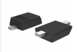
20 kHz kHz 220W W Audio Amplifiers 7.5mm mm 36 pins 36-PowerFSOP (0.295, 7.50mm Width)


20 kHz kHz 220W W Audio Amplifiers 7.5mm mm 36 pins 36-PowerFSOP (0.295, 7.50mm Width)
The TDA7498E is a dual BTL class-D audio amplifier with a single power supply designed for home systems and active speaker applications. The TPA3116D2 is a stereo efficient, digital amplifier power stage for driving speakers up to 100W / 2Ω in mono. This article is going to cover the differences between TDA7498E and TPA3116D2 from the perspective of description, absolute maximum ratings, thermal information, features, and more details.

TPA3116 v/s TDA7498E, real audio output comparison.
- TDA7498E Description
- TPA3116D2 Description
- Comparison of Absolute Maximum Ratings of the TDA7498E vs. TPA3116D2
- Comparison of Thermal Information of the TDA7498E vs. TPA3116D2
- Comparison of features of the TDA7498E vs. TPA3116D2
- Specifications
- Comparison of Electrical Characteristics of the TDA7498E vs. TPA3116D2
- Trend Analysis
- Datasheet PDF
TDA7498E Description
The TDA7498E is a dual BTL class-D audio amplifier with a single power supply designed for home systems and active speaker applications.
It comes in a 36-pin PowerSSO package with exposed pad up (EPU) to facilitate mounting a separate heatsink.
TPA3116D2 Description
The TPA3116D2 is a stereo efficient, digital amplifier power stage for driving speakers up to 100W / 2Ω in mono. The high efficiency of the TPA3130D2 allows it to do 2 × 15 W without an external heat sink on a single layer PCB. The TPA3118D2 can even run 2 × 30 W / 8Ω without a heat sink on a dual-layer PCB, If even higher power is needed the TPA3116D2 does 2 × 50 W / 4 Ωwith a small heatsink attached to its top side PowerPAD. All three devices share the same footprint enabling a single PCB to be used across different power levels.
The TPA3116D2 advanced oscillator/PLL circuit employs multiple switching frequency options to
avoid AM interferences; this is achieved together with an option of either master or slave option, making it possible to synchronize multiple devices.
The TPA3116D2 is fully protected against faults with short-circuit protection and thermal protection as well as overvoltage, Undervoltage, and DC protection. Faults are reported back to the processor to prevent devices from being damaged during overload conditions.
Comparison of Absolute Maximum Ratings of the TDA7498E vs. TPA3116D2
| Symbol | Parameter | Value | Unit |
| VCC | DC supply voltage for pins PVCCA, PVCCB, SVCC | 45 | V |
| VI | Voltage limits for input pins STBY, MUTE, INNA, INPA, INNB, INPB, GAIN, MODE | -0.3 to 4.0 | V |
| Tj | Operating junction temperature | 0 to 150 | °C |
| Top | Operating ambient temperature | 0 to 70 | °C |
| Tstg | Storage temperature | -40 to 150 | °C |
TDA7498E Absolute Maximum Ratings
| MIN | MAX | UNIT | ||
| Supply voltage, VCC | PVCC, AVCC | –0.3 | 30 | V |
| Input voltage, VI | INPL, INNL, INPR, INNR | –0.3 | 6.3 | V |
| PLIMIT, GAIN / SLV, SYNC | –0.3 | GVDD+0.3 | V | |
| AM0, AM1, AM2, MUTE, SDZ, MODSEL | –0.3 | PVCC+0.3 | V | |
| Slew rate, maximum(2) | AM0, AM1, AM2, MUTE, SDZ, MODSEL | 10 | V/ms | |
| Operating free-air temperature, TA | –40 | 85 | °C | |
| Operating junction temperature , TJ | –40 | 150 | °C | |
| Storage temperature, Tstg | –40 | 125 | °C | |
TPA3116D2 Absolute Maximum Ratings
Comparison of Thermal Information of the TDA7498E vs. TPA3116D2
| Symbol | Parameter | Condition | Min | Typ | Max | Unit |
| Iq | Total quiescent current | No LC filter, no load | - | 60 | mA | |
| IqSTBY | Quiescent current in standby | - | - | 1 | µA | |
| VOS | Output offset voltage | Vi = 0, Av = 23.6 dB, no load | -20 | - | 20 | mV |
| IOCP | Overcurrent protection threshold | RL = 0 Ω | 10 | 11 | 14 | A |
| Tj | Junction temperature at thermal shutdown | - | 140 | 150 | 160 | °C |
| Ri | Input resistance | Differential input | 69 | - | kΩ | |
| VUVP | Undervoltage protection threshold | - | - | - | 8 | V |
| RdsON | Power transistor on-resistance | High side | - | 0.15 | - | |
| Low side | - | 0.15 | - | Ω | ||
| Po | Output power | THD = 10% | - | 160 | - | W |
| THD = 1% | - | 125 | - | |||
| Po | Parallel BTL (mono) output power, RL = 3 ohm, Vcc = 36 V | THD = 10% | - | 220 | - | W |
| THD = 1% | - | 170 | - | |||
| η | Efficiency | - | 85 | - | % | |
| THD | Total harmonic distortion | Po = 1 W | - | 0.05 | - | % |
| GV | Closed-loop gain | GAIN < 0.25*VDD | 23.8 | dB | ||
| 0.25*VDD < GAIN < 0.5*VDD | 29.8 | |||||
| 0.5*VDD < GAIN < 0.75*VDD | 33.3 | |||||
| GAIN > 0.75*VDD | 35.8 | |||||
| ΔGV | Gain matching | - | -1 | - | 1 | dB |
| CT | Crosstalk | f = 1 kHz, Po = 1 W | 50 | 60 | - | dB |
| Vn | Total output noise | Inputs shorted and to ground, A Curve | 231 | µV | ||
| Inputs shorted and to ground, f = 20 Hz to 20 kHz | 400 | |||||
| SVRR | Supply voltage rejection ratio | fr = 100 Hz, Vr = 0.5 Vpp, CSVR = 10 µF | - | 55 | - | dB |
| Tr, Tf | Rise and fall times | - | - | 35 | - | ns |
| fSW | Switching frequency | Internal oscillator | 240 | 310 | 400 | kHz |
| fSWR | Output switching frequency range | With internal oscillator by changing ROS (1) C | 240 | - | kHz | |
| VinH | Digital input high (H) | - | 2 | - | - | V |
| VinL | Digital input low (L) | - | - | 0.8 | ||
| Functio n mode | Standby & mute & play | STBY < 0.5 V; MUTE = X | Standby | |||
| STBY > 2.5 V; MUTE < L | Mute | |||||
| STBY > 2.5 V; MUTE > H | Play | |||||
| AMUTE | Mute attenuation | VMUTE < L, VSTBY = H | - | 75 | - | dB |
TDA7498E Thermal Information
| PARAMETER | TEST CONDITIONS | MIN | TYP | MAX | UNIT | |
| | VOS | | Class-D output offset voltage (measured differentially) | VI = 0 V, Gain = 36 dB | 1.5 | 15 | mV | |
| ICC | Quiescent supply current | SDZ = 2 V, No load or filter, PVCC = 12 V | 20 | 35 | mA | |
| SDZ = 2 V, No load or filter, PVCC = 24 V | 32 | 50 | ||||
| ICC(SD) | Quiescent supply current in shutdown mode | SDZ = 0.8 V, No load or filter, PVCC = 12 V | <50 | µA | ||
| SDZ = 0.8 V, No load or filter, PVCC = 24 V | 50 | 400 | ||||
| rDS(on) | Drain-source on-state resistance, measured pin to pin | PVCC = 21 V, Iout = 500 mA, TJ = 25°C | 120 | mΩ | ||
| G | Gain (BTL) | R1 = 5.6 kΩ, R2 = Open | 19 | 20 | 21 | dB |
| R1 = 20 kΩ, R2 = 100 kΩ | 25 | 26 | 27 | |||
| R1 = 39 kΩ, R2 = 100 kΩ | 31 | 32 | 33 | dB | ||
| R1 = 47 kΩ, R2 = 75 kΩ | 35 | 36 | 37 | |||
| G | Gain (SLV) | R1 = 51 kΩ, R2 = 51 kΩ | 19 | 20 | 21 | dB |
| R1 = 75 kΩ, R2 = 47 kΩ | 25 | 26 | 27 | |||
| R1 = 100 kΩ, R2 = 39 kΩ | 31 | 32 | 33 | dB | ||
| R1 = 100 kΩ, R2 = 16 kΩ | 35 | 36 | 37 | |||
| ton | Turn-on time | SDZ = 2 V | 10 | ms | ||
| tOFF | Turn-off time | SDZ = 0.8 V | 2 | µs | ||
| GVDD | Gate drive supply | IGVDD < 200 µA | 6.4 | 6.9 | 7.4 | V |
| VO | Output voltage maximum under PLIMIT control | V(PLIMIT) = 2 V; VI = 1 Vrms | 6.75 | 7.9 | 8.75 | V |
TPA3116D2 Thermal Information
Comparison of features of the TDA7498E vs. TPA3116D2
Features of the 1N4001 include the following:
160-W + 160-W output power at THD = 10%
with RL = 4 Ω and VCC = 36 V
1 x 220 W output power mono parallel BTL
at THD = 10% with RL = 3 Ω and VCC = 36 V
Wide-range single-supply operation
(14 - 36 V)
High efficiency (η = 85%)
Parallel BTL function using the MODE pin
Four selectable, fixed gain settings of
nominally 23.8 dB, 29.8 dB, 33.3 dB and
35.8 dB
Differential inputs minimize common-mode noise
Standby and mute features
Smart protection
Thermal overload protection
Small offset less than 20 mV
Features of the STM32 F4 include the following:
Supports Multiple Output Configurations
– 2 × 50 W Into a 4-Ω BTL Load at 21 V
(TPA3116D2)
– 2 × 30 W Into an 8-Ω BTL Load at 24 V
(TPA3118D2)
– 2 × 15 W Into an 8-Ω BTL Load at 15 V
(TPA3130D2)
Wide Voltage Range: 4.5 V to 26 V
Efficient Class-D Operation
– >90% Power Efficiency Combined With Low
Idle Loss Greatly Reduces Heat Sink Size
– Advanced Modulation Schemes
Multiple Switching Frequencies
– AM Avoidance
– Master and Slave Synchronization
– Up to 1.2-MHz Switching Frequency
Feedback Power-Stage Architecture With High
PSRR Reduces PSU Requirements
Programmable Power Limit
Differential and Single-Ended Inputs
Stereo and Mono Mode With Single-Filter Mono
Configuration
Single Power Supply Reduces Component Count
Integrated Self-Protection Circuits Including
Overvoltage, Undervoltage, Overtemperature, DCDetect,
and Short Circuit With Error Reporting
Thermally Enhanced Packages
– DAD (32-Pin HTSSOP Pad Up)
– DAP (32-Pin HTSSOP Pad Down)
–40°C to 85°C Ambient Temperature Range
Specifications
- TypeParameter
- Lifecycle Status
Lifecycle Status refers to the current stage of an electronic component in its product life cycle, indicating whether it is active, obsolete, or transitioning between these states. An active status means the component is in production and available for purchase. An obsolete status indicates that the component is no longer being manufactured or supported, and manufacturers typically provide a limited time frame for support. Understanding the lifecycle status is crucial for design engineers to ensure continuity and reliability in their projects.
ACTIVE (Last Updated: 8 months ago) - Mount
In electronic components, the term "Mount" typically refers to the method or process of physically attaching or fixing a component onto a circuit board or other electronic device. This can involve soldering, adhesive bonding, or other techniques to secure the component in place. The mounting process is crucial for ensuring proper electrical connections and mechanical stability within the electronic system. Different components may have specific mounting requirements based on their size, shape, and function, and manufacturers provide guidelines for proper mounting procedures to ensure optimal performance and reliability of the electronic device.
Surface Mount - Mounting Type
The "Mounting Type" in electronic components refers to the method used to attach or connect a component to a circuit board or other substrate, such as through-hole, surface-mount, or panel mount.
Surface Mount - Package / Case
refers to the protective housing that encases an electronic component, providing mechanical support, electrical connections, and thermal management.
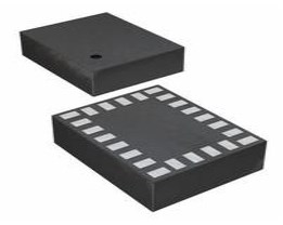
36-PowerFSOP (0.295, 7.50mm Width) - Number of Pins36
- Operating Temperature
The operating temperature is the range of ambient temperature within which a power supply, or any other electrical equipment, operate in. This ranges from a minimum operating temperature, to a peak or maximum operating temperature, outside which, the power supply may fail.
0°C~70°C TA - Packaging
Semiconductor package is a carrier / shell used to contain and cover one or more semiconductor components or integrated circuits. The material of the shell can be metal, plastic, glass or ceramic.
Tube - JESD-609 Code
The "JESD-609 Code" in electronic components refers to a standardized marking code that indicates the lead-free solder composition and finish of electronic components for compliance with environmental regulations.
e3 - Part Status
Parts can have many statuses as they progress through the configuration, analysis, review, and approval stages.
Obsolete - Moisture Sensitivity Level (MSL)
Moisture Sensitivity Level (MSL) is a standardized rating that indicates the susceptibility of electronic components, particularly semiconductors, to moisture-induced damage during storage and the soldering process, defining the allowable exposure time to ambient conditions before they require special handling or baking to prevent failures
1 (Unlimited) - Number of Terminations36
- ECCN Code
An ECCN (Export Control Classification Number) is an alphanumeric code used by the U.S. Bureau of Industry and Security to identify and categorize electronic components and other dual-use items that may require an export license based on their technical characteristics and potential for military use.
EAR99 - TypeClass D
- Terminal Finish
Terminal Finish refers to the surface treatment applied to the terminals or leads of electronic components to enhance their performance and longevity. It can improve solderability, corrosion resistance, and overall reliability of the connection in electronic assemblies. Common finishes include nickel, gold, and tin, each possessing distinct properties suitable for various applications. The choice of terminal finish can significantly impact the durability and effectiveness of electronic devices.
Matte Tin (Sn) - annealed - HTS Code
HTS (Harmonized Tariff Schedule) codes are product classification codes between 8-1 digits. The first six digits are an HS code, and the countries of import assign the subsequent digits to provide additional classification. U.S. HTS codes are 1 digits and are administered by the U.S. International Trade Commission.
8542.33.00.01 - Voltage - Supply
Voltage - Supply refers to the range of voltage levels that an electronic component or circuit is designed to operate with. It indicates the minimum and maximum supply voltage that can be applied for the device to function properly. Providing supply voltages outside this range can lead to malfunction, damage, or reduced performance. This parameter is critical for ensuring compatibility between different components in a circuit.
14V~36V - Terminal Position
In electronic components, the term "Terminal Position" refers to the physical location of the connection points on the component where external electrical connections can be made. These connection points, known as terminals, are typically used to attach wires, leads, or other components to the main body of the electronic component. The terminal position is important for ensuring proper connectivity and functionality of the component within a circuit. It is often specified in technical datasheets or component specifications to help designers and engineers understand how to properly integrate the component into their circuit designs.
DUAL - Terminal Form
Occurring at or forming the end of a series, succession, or the like; closing; concluding.
GULL WING - Peak Reflow Temperature (Cel)
Peak Reflow Temperature (Cel) is a parameter that specifies the maximum temperature at which an electronic component can be exposed during the reflow soldering process. Reflow soldering is a common method used to attach electronic components to a circuit board. The Peak Reflow Temperature is crucial because it ensures that the component is not damaged or degraded during the soldering process. Exceeding the specified Peak Reflow Temperature can lead to issues such as component failure, reduced performance, or even permanent damage to the component. It is important for manufacturers and assemblers to adhere to the recommended Peak Reflow Temperature to ensure the reliability and functionality of the electronic components.
260 - Number of Functions1
- Terminal Pitch
The center distance from one pole to the next.
0.5mm - Time@Peak Reflow Temperature-Max (s)
Time@Peak Reflow Temperature-Max (s) refers to the maximum duration that an electronic component can be exposed to the peak reflow temperature during the soldering process, which is crucial for ensuring reliable solder joint formation without damaging the component.
30 - Base Part Number
The "Base Part Number" (BPN) in electronic components serves a similar purpose to the "Base Product Number." It refers to the primary identifier for a component that captures the essential characteristics shared by a group of similar components. The BPN provides a fundamental way to reference a family or series of components without specifying all the variations and specific details.
TDA7498 - Pin Count
a count of all of the component leads (or pins)
36 - Output Type
The "Output Type" parameter in electronic components refers to the type of signal or data that is produced by the component as an output. This parameter specifies the nature of the output signal, such as analog or digital, and can also include details about the voltage levels, current levels, frequency, and other characteristics of the output signal. Understanding the output type of a component is crucial for ensuring compatibility with other components in a circuit or system, as well as for determining how the output signal can be utilized or processed further. In summary, the output type parameter provides essential information about the nature of the signal that is generated by the electronic component as its output.
1-Channel (Mono) or 2-Channel (Stereo) - Supply Voltage-Min (Vsup)
The parameter "Supply Voltage-Min (Vsup)" in electronic components refers to the minimum voltage level required for the component to operate within its specified performance range. This parameter indicates the lowest voltage that can be safely applied to the component without risking damage or malfunction. It is crucial to ensure that the supply voltage provided to the component meets or exceeds this minimum value to ensure proper functionality and reliability. Failure to adhere to the specified minimum supply voltage may result in erratic behavior, reduced performance, or even permanent damage to the component.
14V - Number of Channels2
- Output Power
That power available at a specified output of a device under specified conditions of operation.
220W - Input Offset Voltage (Vos)
Input Offset Voltage (Vos) is a key parameter in electronic components, particularly in operational amplifiers. It refers to the voltage difference that must be applied between the two input terminals of the amplifier to nullify the output voltage when the input terminals are shorted together. In simpler terms, it represents the voltage required to bring the output of the amplifier to zero when there is no input signal present. Vos is an important parameter as it can introduce errors in the output signal of the amplifier, especially in precision applications where accuracy is crucial. Minimizing Vos is essential to ensure the amplifier operates with high precision and accuracy.
20mV - Bandwidth
In electronic components, "Bandwidth" refers to the range of frequencies over which the component can effectively operate or pass signals without significant loss or distortion. It is a crucial parameter for devices like amplifiers, filters, and communication systems. The bandwidth is typically defined as the difference between the upper and lower frequencies at which the component's performance meets specified criteria, such as a certain level of signal attenuation or distortion. A wider bandwidth indicates that the component can handle a broader range of frequencies, making it more versatile for various applications. Understanding the bandwidth of electronic components is essential for designing and optimizing circuits to ensure proper signal transmission and reception within the desired frequency range.
20 kHz - Voltage Gain
Voltage gain is a measure of how much an electronic component or circuit amplifies an input voltage signal to produce an output voltage signal. It is typically expressed as a ratio or in decibels (dB). A higher voltage gain indicates a greater amplification of the input signal. Voltage gain is an important parameter in amplifiers, where it determines the level of amplification provided by the circuit. It is calculated by dividing the output voltage by the input voltage and is a key factor in determining the overall performance and functionality of electronic devices.
35.8dB - Max Output Power
The maximum output power = the maximum output current × the rated output voltage
220W - Max Output Power x Channels @ Load
Max Output Power x Channels @ Load is a specification that describes the maximum power output that an electronic component, such as an amplifier or audio device, can deliver across a certain number of channels at a specific load impedance. This parameter is important for understanding the capability of the component to drive speakers or other devices effectively. The value is typically expressed in watts and can vary depending on the number of channels being used and the impedance of the load. It helps users determine the compatibility of the component with their audio setup and ensures that the component can provide sufficient power for optimal performance.
220W x 1 @ 3 Ω; 160W x 2 @ 4 Ω - Harmonic Distortion
Harmonic distortion is a common parameter used to describe the quality of audio or electronic signals. It refers to the presence of unwanted harmonics or additional frequencies in the output signal that were not present in the input signal. These harmonics are typically multiples of the original signal frequency and can distort the waveform, affecting the overall sound quality or performance of the electronic component. Lower harmonic distortion values indicate a cleaner and more accurate output signal, while higher distortion levels can result in a more distorted or altered sound. Manufacturers often specify harmonic distortion levels in percentage or decibels to help users understand the quality of the component's output.
10% - Features
In the context of electronic components, the term "Features" typically refers to the specific characteristics or functionalities that a particular component offers. These features can vary depending on the type of component and its intended use. For example, a microcontroller may have features such as built-in memory, analog-to-digital converters, and communication interfaces like UART or SPI.When evaluating electronic components, understanding their features is crucial in determining whether they meet the requirements of a particular project or application. Engineers and designers often look at features such as operating voltage, speed, power consumption, and communication protocols to ensure compatibility and optimal performance.In summary, the "Features" parameter in electronic components describes the unique attributes and capabilities that differentiate one component from another, helping users make informed decisions when selecting components for their electronic designs.
Differential Inputs, Mute, Short-Circuit and Thermal Protection, Standby - Length10.3mm
- Height Seated (Max)
Height Seated (Max) is a parameter in electronic components that refers to the maximum allowable height of the component when it is properly seated or installed on a circuit board or within an enclosure. This specification is crucial for ensuring proper fit and alignment within the overall system design. Exceeding the maximum seated height can lead to mechanical interference, electrical shorts, or other issues that may impact the performance and reliability of the electronic device. Manufacturers provide this information to help designers and engineers select components that will fit within the designated space and function correctly in the intended application.
2.45mm - Width7.5mm
- Radiation Hardening
Radiation hardening is the process of making electronic components and circuits resistant to damage or malfunction caused by high levels of ionizing radiation, especially for environments in outer space (especially beyond the low Earth orbit), around nuclear reactors and particle accelerators, or during nuclear accidents or nuclear warfare.
No - RoHS Status
RoHS means “Restriction of Certain Hazardous Substances” in the “Hazardous Substances Directive” in electrical and electronic equipment.
ROHS3 Compliant
Comparison of Electrical Characteristics of the TDA7498E vs. TPA3116D2
| THERMAL METRIC(1) | TPA3130D2 | TPA3118D2 | TPA3116D2 | |
| DAP(2) | DAP(3) | DAD(4) | UNIT | |
| 32 PINS | 32 PINS | 32 PINS | ||
| RθJA Junction-to-ambient thermal resistance | 36 | 22 | 14 | |
| ψJT Junction-to-top characterization parameter | 0.4 | 0.3 | 1.2 | °C/W |
| ψJB Junction-to-board characterization parameter | 5.9 | 4.7 | 5.7 |
TDA7498E Electrical Characteristics
| Symbol | Parameter | Min | Typ | Max | Unit |
| Rth j-case | Thermal resistance, junction to case | - | 3 | °C/W |
TPA3116D2 Electrical Characteristics
Parts with Similar Specs
Trend Analysis
Datasheet PDF
- Datasheets :
 NC7WZ17P6X Dual Buffer: Package, Applications and Datasheet
01 November 2023472
 STM32F072C8T6 Microcontroller: 48MHz, 48-LQFP, Pinout and Datasheet
21 January 20225245
 LM2575 Replacement & Datasheet: A Cost-Effective Selection Guide
31 January 2026144
 MC1413 Darlington Transistor Array: MC1413, Darlington Array, MC1413 PDF
23 December 20211915
 Understanding STM32G0B0RET6 Troubleshooting Techniques
09 July 2025300
 How to Interface Stepper Motor with PIC16F877A Microcontroller?
01 April 20223633
 PMEG6010CEJ Schottky Diode: Datasheet PDF, Application, Alternative
15 February 20221992
 LSM9DS1TR Gyroscope Magnetometer 9 Axis Sensor I²C SPI Output: Datasheet, Features, and Pinout
07 April 20222797
 Huawei Responded How to Solve the Problem of Chip Supply
29 March 20224069
 Millimeter Wave Radar: Advantages, Types, and Applications
18 October 202119308
 How do Parking Sensors Work?
21 November 202532822
 Will MicroLED replace LCD and OLED?
31 August 20213266
 What are Avalanche Diodes?
02 April 202012740
 What is Feedthrough Capacitor?
06 November 202139696
 Good news | Warm Congratulations to UTMEL Electronic for Obtaining the Letter of Authorization from XKB Connectivity
21 July 20253304
 What is a Tactile Sensor?
21 October 20213788
STMicroelectronics
In Stock: 4
United States
China
Canada
Japan
Russia
Germany
United Kingdom
Singapore
Italy
Hong Kong(China)
Taiwan(China)
France
Korea
Mexico
Netherlands
Malaysia
Austria
Spain
Switzerland
Poland
Thailand
Vietnam
India
United Arab Emirates
Afghanistan
Åland Islands
Albania
Algeria
American Samoa
Andorra
Angola
Anguilla
Antigua & Barbuda
Argentina
Armenia
Aruba
Australia
Azerbaijan
Bahamas
Bahrain
Bangladesh
Barbados
Belarus
Belgium
Belize
Benin
Bermuda
Bhutan
Bolivia
Bonaire, Sint Eustatius and Saba
Bosnia & Herzegovina
Botswana
Brazil
British Indian Ocean Territory
British Virgin Islands
Brunei
Bulgaria
Burkina Faso
Burundi
Cabo Verde
Cambodia
Cameroon
Cayman Islands
Central African Republic
Chad
Chile
Christmas Island
Cocos (Keeling) Islands
Colombia
Comoros
Congo
Congo (DRC)
Cook Islands
Costa Rica
Côte d’Ivoire
Croatia
Cuba
Curaçao
Cyprus
Czechia
Denmark
Djibouti
Dominica
Dominican Republic
Ecuador
Egypt
El Salvador
Equatorial Guinea
Eritrea
Estonia
Eswatini
Ethiopia
Falkland Islands
Faroe Islands
Fiji
Finland
French Guiana
French Polynesia
Gabon
Gambia
Georgia
Ghana
Gibraltar
Greece
Greenland
Grenada
Guadeloupe
Guam
Guatemala
Guernsey
Guinea
Guinea-Bissau
Guyana
Haiti
Honduras
Hungary
Iceland
Indonesia
Iran
Iraq
Ireland
Isle of Man
Israel
Jamaica
Jersey
Jordan
Kazakhstan
Kenya
Kiribati
Kosovo
Kuwait
Kyrgyzstan
Laos
Latvia
Lebanon
Lesotho
Liberia
Libya
Liechtenstein
Lithuania
Luxembourg
Macao(China)
Madagascar
Malawi
Maldives
Mali
Malta
Marshall Islands
Martinique
Mauritania
Mauritius
Mayotte
Micronesia
Moldova
Monaco
Mongolia
Montenegro
Montserrat
Morocco
Mozambique
Myanmar
Namibia
Nauru
Nepal
New Caledonia
New Zealand
Nicaragua
Niger
Nigeria
Niue
Norfolk Island
North Korea
North Macedonia
Northern Mariana Islands
Norway
Oman
Pakistan
Palau
Palestinian Authority
Panama
Papua New Guinea
Paraguay
Peru
Philippines
Pitcairn Islands
Portugal
Puerto Rico
Qatar
Réunion
Romania
Rwanda
Samoa
San Marino
São Tomé & Príncipe
Saudi Arabia
Senegal
Serbia
Seychelles
Sierra Leone
Sint Maarten
Slovakia
Slovenia
Solomon Islands
Somalia
South Africa
South Sudan
Sri Lanka
St Helena, Ascension, Tristan da Cunha
St. Barthélemy
St. Kitts & Nevis
St. Lucia
St. Martin
St. Pierre & Miquelon
St. Vincent & Grenadines
Sudan
Suriname
Svalbard & Jan Mayen
Sweden
Syria
Tajikistan
Tanzania
Timor-Leste
Togo
Tokelau
Tonga
Trinidad & Tobago
Tunisia
Turkey
Turkmenistan
Turks & Caicos Islands
Tuvalu
U.S. Outlying Islands
U.S. Virgin Islands
Uganda
Ukraine
Uruguay
Uzbekistan
Vanuatu
Vatican City
Venezuela
Wallis & Futuna
Yemen
Zambia
Zimbabwe


