
TDA2040 Hi-Fi Audio Power Amplifier: Replacement, Circuit and Datasheet

100mA mA 22W W Audio Amplifiers 25W W 5 pins Pentawatt-5 (Horizontal, Bent and Staggered Leads)


100mA mA 22W W Audio Amplifiers 25W W 5 pins Pentawatt-5 (Horizontal, Bent and Staggered Leads)
TDA2040 is a 20W Hi-Fi audio power amplifier. This post mainly introduces datasheet, pinout, replacement, circuit, power, and other details about the TDA2040 amplifier. Furthermore, there is a huge range of semiconductors, capacitors, resistors, and ICs in stock. Welcome your RFQ!

TDA2040 - HI-FI AUDIO POWER AMPLIFIER | NT Electronics
Overview of TDA2040
The TDA2040 is a Pentawatt audio class AB amplifier with a 22W output power (d=0.5 percent) at Vs = 32V/4. The IC generates a large amount of output current while exhibiting very low harmonic and cross-over distortion. The gadget includes a proprietary short circuit safety system that automatically limits the amount of power dissipated and keeps the output transistors' working points within their safe operating range.
TDA2040 Pinout
TDA2040 Pinout is shown below. The package is called the ‘Pentawatt’ package with 5 output pins.


TDA2040 Pinout
TDA2040 CAD Model
Symbol

TDA2040 Symbol
Footprint

TDA2040 Footprint
Specifications
- TypeParameter
- Mount
In electronic components, the term "Mount" typically refers to the method or process of physically attaching or fixing a component onto a circuit board or other electronic device. This can involve soldering, adhesive bonding, or other techniques to secure the component in place. The mounting process is crucial for ensuring proper electrical connections and mechanical stability within the electronic system. Different components may have specific mounting requirements based on their size, shape, and function, and manufacturers provide guidelines for proper mounting procedures to ensure optimal performance and reliability of the electronic device.
Through Hole - Mounting Type
The "Mounting Type" in electronic components refers to the method used to attach or connect a component to a circuit board or other substrate, such as through-hole, surface-mount, or panel mount.
Through Hole - Package / Case
refers to the protective housing that encases an electronic component, providing mechanical support, electrical connections, and thermal management.
Pentawatt-5 (Horizontal, Bent and Staggered Leads) - Number of Pins5
- Operating Temperature
The operating temperature is the range of ambient temperature within which a power supply, or any other electrical equipment, operate in. This ranges from a minimum operating temperature, to a peak or maximum operating temperature, outside which, the power supply may fail.
-40°C~150°C TJ - Packaging
Semiconductor package is a carrier / shell used to contain and cover one or more semiconductor components or integrated circuits. The material of the shell can be metal, plastic, glass or ceramic.
Tube - JESD-609 Code
The "JESD-609 Code" in electronic components refers to a standardized marking code that indicates the lead-free solder composition and finish of electronic components for compliance with environmental regulations.
e3 - Part Status
Parts can have many statuses as they progress through the configuration, analysis, review, and approval stages.
Obsolete - Moisture Sensitivity Level (MSL)
Moisture Sensitivity Level (MSL) is a standardized rating that indicates the susceptibility of electronic components, particularly semiconductors, to moisture-induced damage during storage and the soldering process, defining the allowable exposure time to ambient conditions before they require special handling or baking to prevent failures
1 (Unlimited) - Number of Terminations5
- ECCN Code
An ECCN (Export Control Classification Number) is an alphanumeric code used by the U.S. Bureau of Industry and Security to identify and categorize electronic components and other dual-use items that may require an export license based on their technical characteristics and potential for military use.
EAR99 - TypeClass AB
- Terminal Finish
Terminal Finish refers to the surface treatment applied to the terminals or leads of electronic components to enhance their performance and longevity. It can improve solderability, corrosion resistance, and overall reliability of the connection in electronic assemblies. Common finishes include nickel, gold, and tin, each possessing distinct properties suitable for various applications. The choice of terminal finish can significantly impact the durability and effectiveness of electronic devices.
Matte Tin (Sn) - Max Power Dissipation
The maximum power that the MOSFET can dissipate continuously under the specified thermal conditions.
25W - Voltage - Supply
Voltage - Supply refers to the range of voltage levels that an electronic component or circuit is designed to operate with. It indicates the minimum and maximum supply voltage that can be applied for the device to function properly. Providing supply voltages outside this range can lead to malfunction, damage, or reduced performance. This parameter is critical for ensuring compatibility between different components in a circuit.
5V~40V ±2.5V~20V - Terminal Position
In electronic components, the term "Terminal Position" refers to the physical location of the connection points on the component where external electrical connections can be made. These connection points, known as terminals, are typically used to attach wires, leads, or other components to the main body of the electronic component. The terminal position is important for ensuring proper connectivity and functionality of the component within a circuit. It is often specified in technical datasheets or component specifications to help designers and engineers understand how to properly integrate the component into their circuit designs.
SINGLE - Peak Reflow Temperature (Cel)
Peak Reflow Temperature (Cel) is a parameter that specifies the maximum temperature at which an electronic component can be exposed during the reflow soldering process. Reflow soldering is a common method used to attach electronic components to a circuit board. The Peak Reflow Temperature is crucial because it ensures that the component is not damaged or degraded during the soldering process. Exceeding the specified Peak Reflow Temperature can lead to issues such as component failure, reduced performance, or even permanent damage to the component. It is important for manufacturers and assemblers to adhere to the recommended Peak Reflow Temperature to ensure the reliability and functionality of the electronic components.
NOT SPECIFIED - Number of Functions1
- Terminal Pitch
The center distance from one pole to the next.
1.7mm - Reach Compliance Code
Reach Compliance Code refers to a designation indicating that electronic components meet the requirements set by the Registration, Evaluation, Authorization, and Restriction of Chemicals (REACH) regulation in the European Union. It signifies that the manufacturer has assessed and managed the chemical substances within the components to ensure safety and environmental protection. This code is vital for compliance with regulations aimed at minimizing risks associated with hazardous substances in electronic products.
not_compliant - Time@Peak Reflow Temperature-Max (s)
Time@Peak Reflow Temperature-Max (s) refers to the maximum duration that an electronic component can be exposed to the peak reflow temperature during the soldering process, which is crucial for ensuring reliable solder joint formation without damaging the component.
NOT SPECIFIED - Base Part Number
The "Base Part Number" (BPN) in electronic components serves a similar purpose to the "Base Product Number." It refers to the primary identifier for a component that captures the essential characteristics shared by a group of similar components. The BPN provides a fundamental way to reference a family or series of components without specifying all the variations and specific details.
TDA2040 - Qualification Status
An indicator of formal certification of qualifications.
Not Qualified - Output Type
The "Output Type" parameter in electronic components refers to the type of signal or data that is produced by the component as an output. This parameter specifies the nature of the output signal, such as analog or digital, and can also include details about the voltage levels, current levels, frequency, and other characteristics of the output signal. Understanding the output type of a component is crucial for ensuring compatibility with other components in a circuit or system, as well as for determining how the output signal can be utilized or processed further. In summary, the output type parameter provides essential information about the nature of the signal that is generated by the electronic component as its output.
1-Channel (Mono) - Operating Supply Voltage
The voltage level by which an electrical system is designated and to which certain operating characteristics of the system are related.
20V - Number of Channels1
- Nominal Supply Current
Nominal current is the same as the rated current. It is the current drawn by the motor while delivering rated mechanical output at its shaft.
100mA - Power Dissipation
the process by which an electronic or electrical device produces heat (energy loss or waste) as an undesirable derivative of its primary action.
25W - Output Power
That power available at a specified output of a device under specified conditions of operation.
22W - Supply Type
Supply Type in electronic components refers to the classification of power sources used to operate the component. It indicates whether the component requires DC or AC power, and if DC, specifies the voltage levels such as low, medium, or high. Different supply types can affect the performance, compatibility, and application of the component in electronic circuits. Understanding the supply type is crucial for proper component selection and integration into electronic designs.
Dual - Input Offset Voltage (Vos)
Input Offset Voltage (Vos) is a key parameter in electronic components, particularly in operational amplifiers. It refers to the voltage difference that must be applied between the two input terminals of the amplifier to nullify the output voltage when the input terminals are shorted together. In simpler terms, it represents the voltage required to bring the output of the amplifier to zero when there is no input signal present. Vos is an important parameter as it can introduce errors in the output signal of the amplifier, especially in precision applications where accuracy is crucial. Minimizing Vos is essential to ensure the amplifier operates with high precision and accuracy.
15V - Nominal Input Voltage
The actual voltage at which a circuit operates can vary from the nominal voltage within a range that permits satisfactory operation of equipment. The word “nominal” means “named”.
15V - Power Supply Rejection Ratio (PSRR)
Power Supply Rejection Ratio (PSRR) is a measure of how well an electronic component, such as an operational amplifier or voltage regulator, can reject changes in its supply voltage. It indicates the ability of the component to maintain a stable output voltage despite fluctuations in the input supply voltage. A higher PSRR value signifies better performance in rejecting noise and variations from the power supply, leading to improved signal integrity and more reliable operation in electronic circuits. PSRR is typically expressed in decibels (dB).
50dB - Gain
In electronic components, "Gain" refers to the ratio of the output signal amplitude to the input signal amplitude. It is a measure of the amplification provided by the component, such as a transistor or operational amplifier. Gain is typically expressed in decibels (dB) or as a numerical value, indicating how much the signal is amplified by the component.A higher gain value indicates a greater amplification of the input signal, while a lower gain value indicates less amplification. Gain is an important parameter in designing and analyzing electronic circuits, as it determines the overall performance and functionality of the system. Different components have different gain characteristics, and understanding the gain of a component is crucial for achieving the desired signal processing or amplification in electronic systems.
80 dB - Max Dual Supply Voltage
A Dual power supply is a regular direct current power supply. It can provide a positive as well as negative voltage. It ensures stable power supply to the device as well as it helps to prevent system damage.
20V - Max Output Power
The maximum output power = the maximum output current × the rated output voltage
22W - Min Dual Supply Voltage
The parameter "Min Dual Supply Voltage" in electronic components refers to the minimum voltage required for the proper operation of a device that uses dual power supplies. Dual power supplies typically consist of a positive and a negative voltage source. The "Min Dual Supply Voltage" specification ensures that both the positive and negative supply voltages are within a certain range to guarantee the device functions correctly. It is important to adhere to this parameter to prevent damage to the component and ensure reliable performance.
2.5V - Dual Supply Voltage
Dual Supply Voltage refers to an electronic component's requirement for two separate power supply voltages, typically one positive and one negative. This configuration is commonly used in operational amplifiers, analog circuits, and certain digital devices to allow for greater signal handling capabilities and improved performance. The use of dual supply voltages enables the device to process bipolar signals, thereby enhancing its functionality in various applications.
18V - Input Bias Current
Input Bias Current refers to the small amount of current that flows into the input terminals of an electronic component, such as an operational amplifier. It is primarily caused by the input impedance of the device and the characteristics of the transistors within it. This current is crucial in determining the accuracy of the analog signal processing, as it can affect the level of voltage offset and signal integrity in the application. In many precise applications, minimizing input bias current is essential to achieve optimal performance.
1μA - Max Output Power x Channels @ Load
Max Output Power x Channels @ Load is a specification that describes the maximum power output that an electronic component, such as an amplifier or audio device, can deliver across a certain number of channels at a specific load impedance. This parameter is important for understanding the capability of the component to drive speakers or other devices effectively. The value is typically expressed in watts and can vary depending on the number of channels being used and the impedance of the load. It helps users determine the compatibility of the component with their audio setup and ensures that the component can provide sufficient power for optimal performance.
22W x 1 @ 4 Ω - Features
In the context of electronic components, the term "Features" typically refers to the specific characteristics or functionalities that a particular component offers. These features can vary depending on the type of component and its intended use. For example, a microcontroller may have features such as built-in memory, analog-to-digital converters, and communication interfaces like UART or SPI.When evaluating electronic components, understanding their features is crucial in determining whether they meet the requirements of a particular project or application. Engineers and designers often look at features such as operating voltage, speed, power consumption, and communication protocols to ensure compatibility and optimal performance.In summary, the "Features" parameter in electronic components describes the unique attributes and capabilities that differentiate one component from another, helping users make informed decisions when selecting components for their electronic designs.
Short-Circuit and Thermal Protection - RoHS Status
RoHS means “Restriction of Certain Hazardous Substances” in the “Hazardous Substances Directive” in electrical and electronic equipment.
ROHS3 Compliant - Lead Free
Lead Free is a term used to describe electronic components that do not contain lead as part of their composition. Lead is a toxic material that can have harmful effects on human health and the environment, so the electronics industry has been moving towards lead-free components to reduce these risks. Lead-free components are typically made using alternative materials such as silver, copper, and tin. Manufacturers must comply with regulations such as the Restriction of Hazardous Substances (RoHS) directive to ensure that their products are lead-free and environmentally friendly.
Lead Free
TDA2040 Schematic Diagram

TDA2040 Schematic Diagram
TDA2040 Features
Ptot - Power Dissipation at Tcase = 75 °C: 25 W
Tstg, Tj - Storage and Junction Temp. -40 to 150°C
Wide-range supply voltage, up to 40 V
Single or split power supply
Short-circuit protection to ground
Thermal shutdown
PO = 25 W @ THD = 0.5%, VS = ±17 V, RL= 4 Ω
PO = 30 W @ THD =10%, VS = ±17 V, RL = 4 Ω
TDA2040 Replacement
| Package | Voltage supply range | Power at 10% 1kHz THD - 8 ohms | Power at 10% 1kHz THD - 4 ohms | Power at 0.5% 1kHz THD - 8 ohms | Power at 0.5% 1kHz THD - 4 ohms | Power at 0.5% 1kHz THD +/-14V - 8 ohms | Peak current limit |
| TDA2006 | '+/-6V to +/-15V (+12V to +30V) | 8W from +/-12V | 12W from +/-12V | 6W from +/-12V | 9W from +/-12V | 11.8W | 3A |
| TDA2030 | '+/-6V to +/-18V (+12V to +34V) | 11W from +/-14V | 18W from +/-14V | 9W from +/-14V | 14W from +/-14V | 9W | 3.5A |
| TDA2030A | '+/-6V to +/-22V (+12V to +44V) | - | - | 12W from +/-16V (40Hz-15kHz) | 18W from +/-16V (40Hz-15kHz) | 9W (40Hz-15kHz) | 3.5A |
| TDA2040 | '+/-2.5V to +/-20V (+5V to +40V) | 16W from +/-16V | 29W from +/-16V | 12W from +/-16V | 22W from +/-16V | 9.2W | 4A |
| TDA2050 | '+/-4.5V to +/-25V (+9V to +50V) | 22W from +/-18V | 35W from +/-18V | 18W from +/-18V | 28W from +/-18V | 12W | 5A |
| LM1875 | '+/-4.5V to +/-25V (+9V to +50V) | - | 25W from +/-25V (1% THD) | - | 8.8W | 4A |
25 Watt Audio Amplifier Circuit using TDA2040

Circuit Schematic
The schematic for a 25-watt audio amplifier is rather straightforward; the TDA2040 amplifies the signal and delivers 25 watts RMS to a 4-ohm loudspeaker. Decoupling filter capacitors C4 and C5 are utilized. C1 and R1 function as filters. R2, R3, and C2 provide the power amplifier with the appropriate feedback. The snubber circuit (R4 and C3) clamps the feedback from the inductive load (Loud Speaker).
The Power amplifier TDA2040 must be appropriately connected to the heatsink while building the circuit. A larger heatsink will produce better results. Also, for a better outcome, audio-grade rated box-type capacitors are recommended.

TDA2040 Test Circuit
To construct the circuit we need the following components:
Vero board (dotted or connected anyone can be used)
Soldering Iron
Solder wire
Nipper and Wire stripper tool
Wires
Aluminum heat sink
17V Rail to Rail power supply with +17V GND -17V power track
4 Ohms 25 Watt speaker
4.7R Resistor 1/2 Watt
680R Resistor 1/4th Watt
22k resistor
10k resistor
100nF / .1uF capacitor 4pcs
22uF capacitor
TDA2040
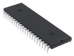
TDA2040 Package Outline

TDA2040 Package Outline
TDA2040 Manufacturer
STMicroelectronics is a globally recognized semiconductor company. They are dedicated to developing semiconductor solutions for various microelectronics applications. STMicroelectronics enjoys unrivaled silicon and system expertise, strong manufacturing strength, IP portfolio, and solid relationships with their strategic partners. Based on these advantages, STMicroelectronics has become a pioneer in System-on-Chip (SoC) technology and its products have a positive effect in realizing today's convergence trends.
Datasheet PDF
- Datasheets :
What can be TDA2040 used for?
The TDA2040 is a monolithic integrated circuit in the Pentawatt® package, intended for use as an audio class-AB amplifier. Typically, it provides 25 W output power into 4 Ω with THD = 0.5% at VS = 34 V. The TDA2040 provides high output current and has very low harmonic and crossover distortion.
Can I use TDA2040 instead TDA2050?
Yes. tda2050, lm675 lm1875 can also be instead but need to be slightly modified (add a 1M resistor).
 LP2951 Voltage Regulator: Pinout, Equivalent and Datasheet
23 October 20212836
 LTC2852 Transceiver: Pinout, Equivalent and Datasheet
24 November 20211031
![282080-1 Rectangular Connectors Housings CONN PLUG BLACK[Video]: Datasheet, Features, and Drawings](https://res.utmel.com/Images/Article/61199823-de3e-4a6f-a253-0628aba362d6.jpg) 282080-1 Rectangular Connectors Housings CONN PLUG BLACK[Video]: Datasheet, Features, and Drawings
282080-1 Rectangular Connectors Housings CONN PLUG BLACK[Video]: Datasheet, Features, and Drawings29 March 20222436
 ESP32S2 WiFi 802.11b/g/n Transceiver Module: Datasheet, Pinout, and Application
13 January 20222103
 ICL7107 ADC Display Driver: Price, Application and Datasheet
25 August 20213102
 WM8960 Stereo CODEC: Pinout, Features and Datasheet
12 February 20224461
 74LS00 Quad 2 Input NAND Gate: Datasheet, Pinout and Schematic
26 October 202113304
 AT89C52 8-Bit Microcontroller: Pin Diagram, AT89C52, Datasheet
15 December 20217210
 Volkswagen Overhauls Semiconductor Sourcing Strategy Amid Supply Challenges
01 September 20232883
 Vibration Isolator: Types and Applications
13 January 202110164
 What is Field Programmable Gate Array(FPGA)?
27 April 20221076
 The Development Trends in the Field of Electronic Component Applications
28 July 20233253
 RGB LED: Circuit, Difference and Application
25 March 20215527
 ITA-3: A Step Towards a Sustainable Future for Global ICT and Economy
14 September 20232593
 The Future of Automated and Additive Manufacturing for Power Electronics
24 May 20233009
 Structure and Working Principle of Field Effect Transistors
07 April 202535727
STMicroelectronics
In Stock
United States
China
Canada
Japan
Russia
Germany
United Kingdom
Singapore
Italy
Hong Kong(China)
Taiwan(China)
France
Korea
Mexico
Netherlands
Malaysia
Austria
Spain
Switzerland
Poland
Thailand
Vietnam
India
United Arab Emirates
Afghanistan
Åland Islands
Albania
Algeria
American Samoa
Andorra
Angola
Anguilla
Antigua & Barbuda
Argentina
Armenia
Aruba
Australia
Azerbaijan
Bahamas
Bahrain
Bangladesh
Barbados
Belarus
Belgium
Belize
Benin
Bermuda
Bhutan
Bolivia
Bonaire, Sint Eustatius and Saba
Bosnia & Herzegovina
Botswana
Brazil
British Indian Ocean Territory
British Virgin Islands
Brunei
Bulgaria
Burkina Faso
Burundi
Cabo Verde
Cambodia
Cameroon
Cayman Islands
Central African Republic
Chad
Chile
Christmas Island
Cocos (Keeling) Islands
Colombia
Comoros
Congo
Congo (DRC)
Cook Islands
Costa Rica
Côte d’Ivoire
Croatia
Cuba
Curaçao
Cyprus
Czechia
Denmark
Djibouti
Dominica
Dominican Republic
Ecuador
Egypt
El Salvador
Equatorial Guinea
Eritrea
Estonia
Eswatini
Ethiopia
Falkland Islands
Faroe Islands
Fiji
Finland
French Guiana
French Polynesia
Gabon
Gambia
Georgia
Ghana
Gibraltar
Greece
Greenland
Grenada
Guadeloupe
Guam
Guatemala
Guernsey
Guinea
Guinea-Bissau
Guyana
Haiti
Honduras
Hungary
Iceland
Indonesia
Iran
Iraq
Ireland
Isle of Man
Israel
Jamaica
Jersey
Jordan
Kazakhstan
Kenya
Kiribati
Kosovo
Kuwait
Kyrgyzstan
Laos
Latvia
Lebanon
Lesotho
Liberia
Libya
Liechtenstein
Lithuania
Luxembourg
Macao(China)
Madagascar
Malawi
Maldives
Mali
Malta
Marshall Islands
Martinique
Mauritania
Mauritius
Mayotte
Micronesia
Moldova
Monaco
Mongolia
Montenegro
Montserrat
Morocco
Mozambique
Myanmar
Namibia
Nauru
Nepal
New Caledonia
New Zealand
Nicaragua
Niger
Nigeria
Niue
Norfolk Island
North Korea
North Macedonia
Northern Mariana Islands
Norway
Oman
Pakistan
Palau
Palestinian Authority
Panama
Papua New Guinea
Paraguay
Peru
Philippines
Pitcairn Islands
Portugal
Puerto Rico
Qatar
Réunion
Romania
Rwanda
Samoa
San Marino
São Tomé & Príncipe
Saudi Arabia
Senegal
Serbia
Seychelles
Sierra Leone
Sint Maarten
Slovakia
Slovenia
Solomon Islands
Somalia
South Africa
South Sudan
Sri Lanka
St Helena, Ascension, Tristan da Cunha
St. Barthélemy
St. Kitts & Nevis
St. Lucia
St. Martin
St. Pierre & Miquelon
St. Vincent & Grenadines
Sudan
Suriname
Svalbard & Jan Mayen
Sweden
Syria
Tajikistan
Tanzania
Timor-Leste
Togo
Tokelau
Tonga
Trinidad & Tobago
Tunisia
Turkey
Turkmenistan
Turks & Caicos Islands
Tuvalu
U.S. Outlying Islands
U.S. Virgin Islands
Uganda
Ukraine
Uruguay
Uzbekistan
Vanuatu
Vatican City
Venezuela
Wallis & Futuna
Yemen
Zambia
Zimbabwe


