
 Product
 Brand
Brand Articles
 Tools
Tools
2N3771 Transistor: 2N3771 NPN Power Transistor, Datasheet, Pinout


TRANS NPN 40V 30A TO-3
The 2N3771 is a high current switching transistor that has a collector current of 30A. This article will cover its datasheet, pinout, replacement about 2N3771. Welcome your RFQ!

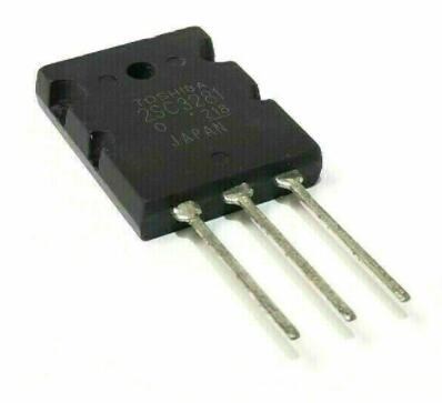
TO-3 package rendering of 2N3771 high gain pass transistor
2N3771 Pinout

2N3771 Pinout
Pin Number | Pin Name | Description |
1 | Base | Controls the biasing of the transistor, Used to turn ON or OFF the transistor |
2 | Collector | Current flows in through collector, normally connected to load |
3 | Emitter | Current Drains out through emitter, normally connected to ground |
2N3771 CAD Model
Symbol

2N3771 Symbol
Footprint

2N3771 Footprint
2N3771 Description
The 2N3771 is a high-power NPN transistor that can handle up to 30A of collector current. The transistor also has a low base threshold voltage of less than 5V and a high collector to emitter voltage of 40V, making it appropriate for high current switching devices.
Despite the fact that the transistor has a very low gain of 60 maximum, it is still utilized in a few linear amplifiers due to the high current. It's most typically found in power supply circuits and in inductive load switching. The transistor is packaged in a To-3 package, which means it has only two leads: Base and Emitter, with the collector acting as the transistor's body. Because the collector will be carrying a huge amount of current, the body will act as a heat sink due to its enormous surface area. If you're utilizing them on a PCB, the collector connection is formed by securing them with nuts. If you're using a computer, there are also mounting kits and connections available.
2N3771 Feature
High Power NPN Transistor
DC Current Gain (hFE) 15 to 60
Continuous Collector current (IC) is 30A
Collector-Emitter voltage (VCE) is 40 V
Collector-Base voltage (VCB) is 50V
Emitter Base Voltage (VBE) is 5V
Available in To-3 Package
2N3771 Application
Linear switching circuits
Small Amplifiers
Power supply circuits
Inductive load switching
high current switching (up to 20A) loads
2N3771 Alternatives
The alternatives for 2N3771:
SK9134
NTE181
2N5302
Specifications
- TypeParameter
- Mount
In electronic components, the term "Mount" typically refers to the method or process of physically attaching or fixing a component onto a circuit board or other electronic device. This can involve soldering, adhesive bonding, or other techniques to secure the component in place. The mounting process is crucial for ensuring proper electrical connections and mechanical stability within the electronic system. Different components may have specific mounting requirements based on their size, shape, and function, and manufacturers provide guidelines for proper mounting procedures to ensure optimal performance and reliability of the electronic device.
Chassis Mount, Through Hole - Mounting Type
The "Mounting Type" in electronic components refers to the method used to attach or connect a component to a circuit board or other substrate, such as through-hole, surface-mount, or panel mount.
Chassis Mount - Package / Case
refers to the protective housing that encases an electronic component, providing mechanical support, electrical connections, and thermal management.
TO-204AA, TO-3 - Number of Pins2
- Collector-Emitter Breakdown Voltage40V
- Collector-Emitter Saturation Voltage2V
- Number of Elements1
- hFEMin5
- Packaging
Semiconductor package is a carrier / shell used to contain and cover one or more semiconductor components or integrated circuits. The material of the shell can be metal, plastic, glass or ceramic.
Tube - JESD-609 Code
The "JESD-609 Code" in electronic components refers to a standardized marking code that indicates the lead-free solder composition and finish of electronic components for compliance with environmental regulations.
e3 - Part Status
Parts can have many statuses as they progress through the configuration, analysis, review, and approval stages.
Obsolete - Moisture Sensitivity Level (MSL)
Moisture Sensitivity Level (MSL) is a standardized rating that indicates the susceptibility of electronic components, particularly semiconductors, to moisture-induced damage during storage and the soldering process, defining the allowable exposure time to ambient conditions before they require special handling or baking to prevent failures
1 (Unlimited) - Number of Terminations2
- ECCN Code
An ECCN (Export Control Classification Number) is an alphanumeric code used by the U.S. Bureau of Industry and Security to identify and categorize electronic components and other dual-use items that may require an export license based on their technical characteristics and potential for military use.
EAR99 - Terminal Finish
Terminal Finish refers to the surface treatment applied to the terminals or leads of electronic components to enhance their performance and longevity. It can improve solderability, corrosion resistance, and overall reliability of the connection in electronic assemblies. Common finishes include nickel, gold, and tin, each possessing distinct properties suitable for various applications. The choice of terminal finish can significantly impact the durability and effectiveness of electronic devices.
Tin (Sn) - Max Operating Temperature
The Maximum Operating Temperature is the maximum body temperature at which the thermistor is designed to operate for extended periods of time with acceptable stability of its electrical characteristics.
200°C - Min Operating Temperature
The "Min Operating Temperature" parameter in electronic components refers to the lowest temperature at which the component is designed to operate effectively and reliably. This parameter is crucial for ensuring the proper functioning and longevity of the component, as operating below this temperature may lead to performance issues or even damage. Manufacturers specify the minimum operating temperature to provide guidance to users on the environmental conditions in which the component can safely operate. It is important to adhere to this parameter to prevent malfunctions and ensure the overall reliability of the electronic system.
-65°C - Voltage - Rated DC
Voltage - Rated DC is a parameter that specifies the maximum direct current (DC) voltage that an electronic component can safely handle without being damaged. This rating is crucial for ensuring the proper functioning and longevity of the component in a circuit. Exceeding the rated DC voltage can lead to overheating, breakdown, or even permanent damage to the component. It is important to carefully consider this parameter when designing or selecting components for a circuit to prevent any potential issues related to voltage overload.
40V - Max Power Dissipation
The maximum power that the MOSFET can dissipate continuously under the specified thermal conditions.
150W - Terminal Position
In electronic components, the term "Terminal Position" refers to the physical location of the connection points on the component where external electrical connections can be made. These connection points, known as terminals, are typically used to attach wires, leads, or other components to the main body of the electronic component. The terminal position is important for ensuring proper connectivity and functionality of the component within a circuit. It is often specified in technical datasheets or component specifications to help designers and engineers understand how to properly integrate the component into their circuit designs.
BOTTOM - Terminal Form
Occurring at or forming the end of a series, succession, or the like; closing; concluding.
PIN/PEG - Current Rating
Current rating is the maximum current that a fuse will carry for an indefinite period without too much deterioration of the fuse element.
30A - Frequency
In electronic components, the parameter "Frequency" refers to the rate at which a signal oscillates or cycles within a given period of time. It is typically measured in Hertz (Hz) and represents how many times a signal completes a full cycle in one second. Frequency is a crucial aspect in electronic components as it determines the behavior and performance of various devices such as oscillators, filters, and communication systems. Understanding the frequency characteristics of components is essential for designing and analyzing electronic circuits to ensure proper functionality and compatibility with other components in a system.
200kHz - Base Part Number
The "Base Part Number" (BPN) in electronic components serves a similar purpose to the "Base Product Number." It refers to the primary identifier for a component that captures the essential characteristics shared by a group of similar components. The BPN provides a fundamental way to reference a family or series of components without specifying all the variations and specific details.
2N37 - Element Configuration
The distribution of electrons of an atom or molecule (or other physical structure) in atomic or molecular orbitals.
Single - Power Dissipation
the process by which an electronic or electrical device produces heat (energy loss or waste) as an undesirable derivative of its primary action.
150W - Case Connection
Case Connection refers to the method by which an electronic component's case or housing is connected to the electrical circuit. This connection is important for grounding purposes, mechanical stability, and heat dissipation. The case connection can vary depending on the type of component and its intended application. It is crucial to ensure a secure and reliable case connection to maintain the overall performance and safety of the electronic device.
COLLECTOR - Transistor Application
In the context of electronic components, the parameter "Transistor Application" refers to the specific purpose or function for which a transistor is designed and used. Transistors are semiconductor devices that can amplify or switch electronic signals and are commonly used in various electronic circuits. The application of a transistor can vary widely depending on its design and characteristics, such as whether it is intended for audio amplification, digital logic, power control, or radio frequency applications. Understanding the transistor application is important for selecting the right type of transistor for a particular circuit or system to ensure optimal performance and functionality.
SWITCHING - Gain Bandwidth Product
The gain–bandwidth product (designated as GBWP, GBW, GBP, or GB) for an amplifier is the product of the amplifier's bandwidth and the gain at which the bandwidth is measured.
200 kHz - Polarity/Channel Type
In electronic components, the parameter "Polarity/Channel Type" refers to the characteristic that determines the direction of current flow or the type of signal that can be accommodated by the component. For components like diodes and transistors, polarity indicates the direction in which current can flow through the component, such as forward bias or reverse bias for diodes. For components like MOSFETs or JFETs, the channel type refers to whether the component is an N-channel or P-channel device, which determines the type of charge carriers that carry current through the component. Understanding the polarity or channel type of a component is crucial for proper circuit design and ensuring that the component is connected correctly to achieve the desired functionality.
NPN - Transistor Type
Transistor type refers to the classification of transistors based on their operation and construction. The two primary types are bipolar junction transistors (BJTs) and field-effect transistors (FETs). BJTs use current to control the flow of current, while FETs utilize voltage to control current flow. Each type has its own subtypes, such as NPN and PNP for BJTs, and MOSFETs and JFETs for FETs, impacting their applications and characteristics in electronic circuits.
NPN - Collector Emitter Voltage (VCEO)
Collector-Emitter Voltage (VCEO) is a key parameter in electronic components, particularly in transistors. It refers to the maximum voltage that can be applied between the collector and emitter terminals of a transistor while the base terminal is open or not conducting. Exceeding this voltage limit can lead to breakdown and potential damage to the transistor. VCEO is crucial for ensuring the safe and reliable operation of the transistor within its specified limits. Designers must carefully consider VCEO when selecting transistors for a circuit to prevent overvoltage conditions that could compromise the performance and longevity of the component.
40V - Max Collector Current
Max Collector Current is a parameter used to specify the maximum amount of current that can safely flow through the collector terminal of a transistor or other electronic component without causing damage. It is typically expressed in units of amperes (A) and is an important consideration when designing circuits to ensure that the component operates within its safe operating limits. Exceeding the specified max collector current can lead to overheating, degradation of performance, or even permanent damage to the component. Designers must carefully consider this parameter when selecting components and designing circuits to ensure reliable and safe operation.
30A - DC Current Gain (hFE) (Min) @ Ic, Vce
The parameter "DC Current Gain (hFE) (Min) @ Ic, Vce" in electronic components refers to the minimum value of the DC current gain, denoted as hFE, under specific operating conditions of collector current (Ic) and collector-emitter voltage (Vce). The DC current gain hFE represents the ratio of the collector current to the base current in a bipolar junction transistor (BJT), indicating the amplification capability of the transistor. The minimum hFE value at a given Ic and Vce helps determine the transistor's performance and efficiency in amplifying signals within a circuit. Designers use this parameter to ensure proper transistor selection and performance in various electronic applications.
15 @ 15A 4V - Current - Collector Cutoff (Max)
The parameter "Current - Collector Cutoff (Max)" refers to the maximum current at which a transistor or other electronic component will cease to conduct current between the collector and emitter terminals. This parameter is important in determining the maximum current that can flow through the component when it is in the cutoff state. Exceeding this maximum cutoff current can lead to malfunction or damage of the component. It is typically specified in the component's datasheet and is crucial for proper circuit design and operation.
10mA - Vce Saturation (Max) @ Ib, Ic
The parameter "Vce Saturation (Max) @ Ib, Ic" in electronic components refers to the maximum voltage drop across the collector-emitter junction when the transistor is in saturation mode. This parameter is specified at a certain base current (Ib) and collector current (Ic) levels. It indicates the minimum voltage required to keep the transistor fully conducting in saturation mode, ensuring that the transistor operates efficiently and does not enter the cutoff region. Designers use this parameter to ensure proper transistor operation and to prevent overheating or damage to the component.
4V @ 6A, 30A - Transition Frequency
Transition Frequency in electronic components refers to the frequency at which a device can transition from one state to another, typically defining the upper limit of its operating frequency. It is a critical parameter in determining the speed and performance of active components like transistors and integrated circuits. This frequency is influenced by factors such as capacitance, resistance, and the inherent characteristics of the materials used in the component's construction. Understanding transition frequency is essential for optimizing circuit designs and ensuring reliable signal processing in various applications.
0.2MHz - Max Breakdown Voltage
The "Max Breakdown Voltage" of an electronic component refers to the maximum voltage that the component can withstand across its terminals before it breaks down and allows current to flow uncontrollably. This parameter is crucial in determining the operating limits and safety margins of the component in a circuit. Exceeding the maximum breakdown voltage can lead to permanent damage or failure of the component. It is typically specified by the manufacturer in datasheets to guide engineers and designers in selecting the appropriate components for their applications.
400V - Collector Base Voltage (VCBO)
Collector Base Voltage (VCBO) is the maximum allowable voltage that can be applied between the collector and base terminals of a bipolar junction transistor when the emitter is open. It is a critical parameter that determines the voltage rating of the transistor and helps prevent breakdown in the collector-base junction. Exceeding this voltage can lead to permanent damage or failure of the component.
50V - Emitter Base Voltage (VEBO)
Emitter Base Voltage (VEBO) is a parameter used in electronic components, particularly in transistors. It refers to the maximum voltage that can be applied between the emitter and base terminals of a transistor without causing damage to the device. Exceeding this voltage limit can lead to breakdown of the transistor and potential failure. VEBO is an important specification to consider when designing circuits to ensure the proper operation and reliability of the components. It is typically provided in the datasheet of the transistor and should be carefully observed to prevent any potential damage during operation.
5V - VCEsat-Max
VCEsat-Max refers to the maximum collector-emitter saturation voltage of a bipolar junction transistor (BJT) or an insulated gate bipolar transistor (IGBT). It is a crucial parameter that indicates the minimum voltage drop across the collector-emitter junction when the transistor is in saturation mode. This parameter is important for determining the efficiency and performance of the transistor in switching applications. A lower VCEsat-Max value indicates better performance and reduced power losses in the transistor during operation. Designers often consider this parameter when selecting transistors for applications where minimizing power dissipation is critical.
4 V - REACH SVHC
The parameter "REACH SVHC" in electronic components refers to the compliance with the Registration, Evaluation, Authorization, and Restriction of Chemicals (REACH) regulation regarding Substances of Very High Concern (SVHC). SVHCs are substances that may have serious effects on human health or the environment, and their use is regulated under REACH to ensure their safe handling and minimize their impact.Manufacturers of electronic components need to declare if their products contain any SVHCs above a certain threshold concentration and provide information on the safe use of these substances. This information allows customers to make informed decisions about the potential risks associated with using the components and take appropriate measures to mitigate any hazards.Ensuring compliance with REACH SVHC requirements is essential for electronics manufacturers to meet regulatory standards, protect human health and the environment, and maintain transparency in their supply chain. It also demonstrates a commitment to sustainability and responsible manufacturing practices in the electronics industry.
No SVHC - Radiation Hardening
Radiation hardening is the process of making electronic components and circuits resistant to damage or malfunction caused by high levels of ionizing radiation, especially for environments in outer space (especially beyond the low Earth orbit), around nuclear reactors and particle accelerators, or during nuclear accidents or nuclear warfare.
No - RoHS Status
RoHS means “Restriction of Certain Hazardous Substances” in the “Hazardous Substances Directive” in electrical and electronic equipment.
ROHS3 Compliant - Lead Free
Lead Free is a term used to describe electronic components that do not contain lead as part of their composition. Lead is a toxic material that can have harmful effects on human health and the environment, so the electronics industry has been moving towards lead-free components to reduce these risks. Lead-free components are typically made using alternative materials such as silver, copper, and tin. Manufacturers must comply with regulations such as the Restriction of Hazardous Substances (RoHS) directive to ensure that their products are lead-free and environmentally friendly.
Lead Free
Parts with Similar Specs
2N3771 Package


2N3771 Package
2N3771 Manufacturer
Datasheet PDF
- Datasheets :
Trend Analysis
What is the gain of the 2N3771 transistor?
60 maximum.
Where is the transistor most commonly used?
Power supply circuits and for switching inductive loads.
What package does the transistor come in?
To-3
What happens to the body of the transistor due to its large surface area?
The body will act as a heat sink.
What can you use if you are using them on testing boards?
Mounting kits and wires.
What is the difference between PNP and NPN?
PNP sensors produce a positive output to your industrial controls input, while NPN sensors produce a negative signal during an “on” state. ... NPN, or “sinking” output sensors, work in the opposite way, sinking ground voltage to input when it's on.
How do NPN transistors work?
An NPN transistor consists of a layer of P-doped semiconductor between two layers of N-doped material, where electrons are passed from the emitter to the collector instead. The emitter then “emits” electrons into the base, with the base controlling the no. of electrons the emitter emits.
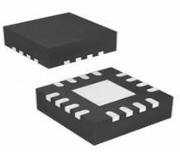 TLV62130ARGTR: 16-VFQFN, 3A, 5V, Pinout
26 February 20221282
 2SC3281 NPN Power Transistor: 200V Power Transistor, Datasheet pdf and Equivalent
22 December 20217393
 LM3S316IGZ25C2T Stellaris® Microcontroller: Extensive Technical Analysis
29 February 2024139
 A Comprehensive Guide to LTC7000MPMSE#TRPBF Gate Driver
06 March 2024227
 Arduino Uno R4 WiFi: Description, Features and applications
06 October 20235879
 1N4744A Zener Diodes: Circuit, Pinout, and Datasheet
08 November 20213986
 Renesas RL78/I1E Microcontroller Series: Advanced Features and Applications
29 February 2024672
 L298P: 42V,13mA, Pinout and Datasheet
23 February 20223134
 3 Under-the-Radar Semiconductor Stocks Poised for Massive Growth
06 October 20233279
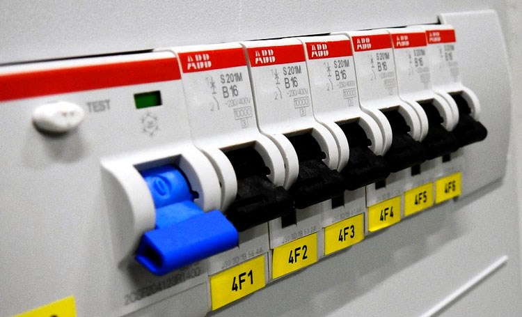 Circuit Breaker: Working Principle, Types and Structure
21 November 202511270
 The Era of UFS 4.0, Announced?
06 May 20227127
 An Analysis of Current-Source Inverters Using High-Frequency WBG Switches
09 May 20234834
 How do Solar Cells Work?
20 November 20203010
 What is a Delay Circuit? 6 Types of Delay Circuits Explained
28 March 202549777
 What is Optical Module?
08 December 20216599
![PMIC: Basic Types and Applications [Video]](https://res.utmel.com/Images/Article/596928b4-5505-4751-b95b-54949cc0bf7b.jpg) PMIC: Basic Types and Applications [Video]
PMIC: Basic Types and Applications [Video]27 October 20205074
STMicroelectronics
In Stock: 10000
United States
China
Canada
Japan
Russia
Germany
United Kingdom
Singapore
Italy
Hong Kong(China)
Taiwan(China)
France
Korea
Mexico
Netherlands
Malaysia
Austria
Spain
Switzerland
Poland
Thailand
Vietnam
India
United Arab Emirates
Afghanistan
Åland Islands
Albania
Algeria
American Samoa
Andorra
Angola
Anguilla
Antigua & Barbuda
Argentina
Armenia
Aruba
Australia
Azerbaijan
Bahamas
Bahrain
Bangladesh
Barbados
Belarus
Belgium
Belize
Benin
Bermuda
Bhutan
Bolivia
Bonaire, Sint Eustatius and Saba
Bosnia & Herzegovina
Botswana
Brazil
British Indian Ocean Territory
British Virgin Islands
Brunei
Bulgaria
Burkina Faso
Burundi
Cabo Verde
Cambodia
Cameroon
Cayman Islands
Central African Republic
Chad
Chile
Christmas Island
Cocos (Keeling) Islands
Colombia
Comoros
Congo
Congo (DRC)
Cook Islands
Costa Rica
Côte d’Ivoire
Croatia
Cuba
Curaçao
Cyprus
Czechia
Denmark
Djibouti
Dominica
Dominican Republic
Ecuador
Egypt
El Salvador
Equatorial Guinea
Eritrea
Estonia
Eswatini
Ethiopia
Falkland Islands
Faroe Islands
Fiji
Finland
French Guiana
French Polynesia
Gabon
Gambia
Georgia
Ghana
Gibraltar
Greece
Greenland
Grenada
Guadeloupe
Guam
Guatemala
Guernsey
Guinea
Guinea-Bissau
Guyana
Haiti
Honduras
Hungary
Iceland
Indonesia
Iran
Iraq
Ireland
Isle of Man
Israel
Jamaica
Jersey
Jordan
Kazakhstan
Kenya
Kiribati
Kosovo
Kuwait
Kyrgyzstan
Laos
Latvia
Lebanon
Lesotho
Liberia
Libya
Liechtenstein
Lithuania
Luxembourg
Macao(China)
Madagascar
Malawi
Maldives
Mali
Malta
Marshall Islands
Martinique
Mauritania
Mauritius
Mayotte
Micronesia
Moldova
Monaco
Mongolia
Montenegro
Montserrat
Morocco
Mozambique
Myanmar
Namibia
Nauru
Nepal
New Caledonia
New Zealand
Nicaragua
Niger
Nigeria
Niue
Norfolk Island
North Korea
North Macedonia
Northern Mariana Islands
Norway
Oman
Pakistan
Palau
Palestinian Authority
Panama
Papua New Guinea
Paraguay
Peru
Philippines
Pitcairn Islands
Portugal
Puerto Rico
Qatar
Réunion
Romania
Rwanda
Samoa
San Marino
São Tomé & Príncipe
Saudi Arabia
Senegal
Serbia
Seychelles
Sierra Leone
Sint Maarten
Slovakia
Slovenia
Solomon Islands
Somalia
South Africa
South Sudan
Sri Lanka
St Helena, Ascension, Tristan da Cunha
St. Barthélemy
St. Kitts & Nevis
St. Lucia
St. Martin
St. Pierre & Miquelon
St. Vincent & Grenadines
Sudan
Suriname
Svalbard & Jan Mayen
Sweden
Syria
Tajikistan
Tanzania
Timor-Leste
Togo
Tokelau
Tonga
Trinidad & Tobago
Tunisia
Turkey
Turkmenistan
Turks & Caicos Islands
Tuvalu
U.S. Outlying Islands
U.S. Virgin Islands
Uganda
Ukraine
Uruguay
Uzbekistan
Vanuatu
Vatican City
Venezuela
Wallis & Futuna
Yemen
Zambia
Zimbabwe


