
 Product
 Brand
Brand Articles
 Tools
Tools
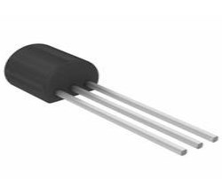
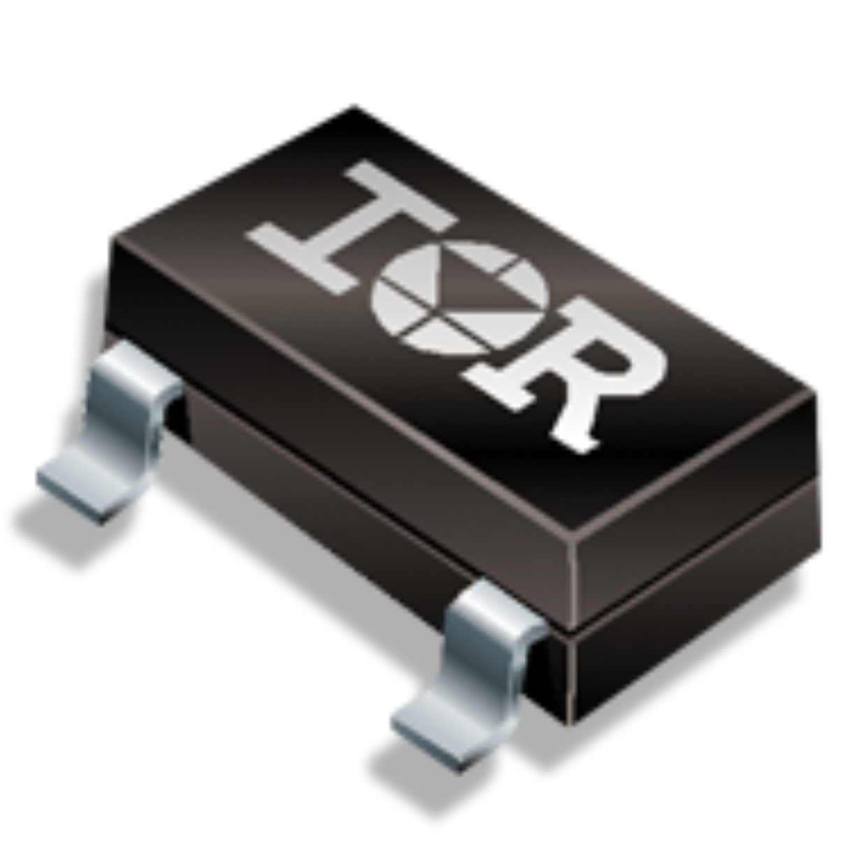
2SC1815 NPN-Transistor : Pinout, Equivalents and Datasheet

2SC1815 datasheet pdf and Transistors - Bipolar (BJT) - Single product details from Central Semiconductor stock available at Utmel


Hello everyone, I am Rose. Today I will introduce 2SC1815 to you. The 2SC1815 is a 50V 150mA general purpose NPN low-power silicon transistor with a maximum gain value of 700. This article mainly introduces pinout, equivalents, datasheet, and other detailed information about Central Semiconductor 2SC1815.
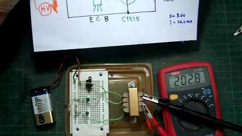
High volt shock by transistor 2SC1815
2SC1815 Description
The 2SC1815 is a 50V 150mA general purpose NPN low-power silicon transistor with a maximum gain value of 700. It is produced by Central Semiconductor. The tube withstand voltage is 40V, Pcm=400mW, Icm=150mA, and it adopts TO-92 package. The transistor polarity is NPN. This makes the transistor suitable for amplifier applications.
2SC1815 Pinout

2SC1815 Pinout
| Pin Number | Pin Name | Description |
| 1 | Emitter | Current Drains out through emitter, normally connected to ground |
| 2 | Collector | Current flows in through collector, normally connected to load |
| 3 | Base | Controls the biasing of the transistor, Used to turn ON or OFF the transistor |
2SC1815 Pin Description
2SC1815 CAD Model

Symbol

Footprint

3D Model
2SC1815 Features
●General Purpose NPN Transistor
●DC Current Gain (hFE) 70 to 700
●Continuous Collector current (IC) is 150mA
●Collector-Emitter voltage (VCE) is 50V
●Collector-Base voltage (VCB) is 60V
●Emitter-base breakdown voltage (VEBO): 5V
●Collector-emitter saturation voltage drop (VCE): 0.25V
●Transition Frequency: 80MHz
●Base current (IB): 50mA
●Power dissipation (PC): 400mW
●Available in To-92 Package
Specifications
- TypeParameter
- Factory Lead Time8 Weeks
- Surface Mount
having leads that are designed to be soldered on the side of a circuit board that the body of the component is mounted on.
NO - Transistor Element Material
The "Transistor Element Material" parameter in electronic components refers to the material used to construct the transistor within the component. Transistors are semiconductor devices that amplify or switch electronic signals and are a fundamental building block in electronic circuits. The material used for the transistor element can significantly impact the performance and characteristics of the component. Common materials used for transistor elements include silicon, germanium, and gallium arsenide, each with its own unique properties and suitability for different applications. The choice of transistor element material is crucial in designing electronic components to meet specific performance requirements such as speed, power efficiency, and temperature tolerance.
SILICON - Collector-Emitter Breakdown Voltage50V
- Number of Elements1
- Power Dissipation (Max)400mW
- Published2016
- Part Status
Parts can have many statuses as they progress through the configuration, analysis, review, and approval stages.
Active - Number of Terminations3
- ECCN Code
An ECCN (Export Control Classification Number) is an alphanumeric code used by the U.S. Bureau of Industry and Security to identify and categorize electronic components and other dual-use items that may require an export license based on their technical characteristics and potential for military use.
EAR99 - Terminal Position
In electronic components, the term "Terminal Position" refers to the physical location of the connection points on the component where external electrical connections can be made. These connection points, known as terminals, are typically used to attach wires, leads, or other components to the main body of the electronic component. The terminal position is important for ensuring proper connectivity and functionality of the component within a circuit. It is often specified in technical datasheets or component specifications to help designers and engineers understand how to properly integrate the component into their circuit designs.
BOTTOM - Terminal Form
Occurring at or forming the end of a series, succession, or the like; closing; concluding.
THROUGH-HOLE - JESD-30 Code
JESD-30 Code refers to a standardized descriptive designation system established by JEDEC for semiconductor-device packages. This system provides a systematic method for generating designators that convey essential information about the package's physical characteristics, such as size and shape, which aids in component identification and selection. By using JESD-30 codes, manufacturers and engineers can ensure consistency and clarity in the specification of semiconductor packages across various applications and industries.
O-PBCY-T3 - Configuration
The parameter "Configuration" in electronic components refers to the specific arrangement or setup of the components within a circuit or system. It encompasses how individual elements are interconnected and their physical layout. Configuration can affect the functionality, performance, and efficiency of the electronic system, and may influence factors such as signal flow, impedance, and power distribution. Understanding the configuration is essential for design, troubleshooting, and optimizing electronic devices.
SINGLE - Transistor Application
In the context of electronic components, the parameter "Transistor Application" refers to the specific purpose or function for which a transistor is designed and used. Transistors are semiconductor devices that can amplify or switch electronic signals and are commonly used in various electronic circuits. The application of a transistor can vary widely depending on its design and characteristics, such as whether it is intended for audio amplification, digital logic, power control, or radio frequency applications. Understanding the transistor application is important for selecting the right type of transistor for a particular circuit or system to ensure optimal performance and functionality.
AMPLIFIER - Polarity/Channel Type
In electronic components, the parameter "Polarity/Channel Type" refers to the characteristic that determines the direction of current flow or the type of signal that can be accommodated by the component. For components like diodes and transistors, polarity indicates the direction in which current can flow through the component, such as forward bias or reverse bias for diodes. For components like MOSFETs or JFETs, the channel type refers to whether the component is an N-channel or P-channel device, which determines the type of charge carriers that carry current through the component. Understanding the polarity or channel type of a component is crucial for proper circuit design and ensuring that the component is connected correctly to achieve the desired functionality.
NPN - Collector Emitter Voltage (VCEO)
Collector-Emitter Voltage (VCEO) is a key parameter in electronic components, particularly in transistors. It refers to the maximum voltage that can be applied between the collector and emitter terminals of a transistor while the base terminal is open or not conducting. Exceeding this voltage limit can lead to breakdown and potential damage to the transistor. VCEO is crucial for ensuring the safe and reliable operation of the transistor within its specified limits. Designers must carefully consider VCEO when selecting transistors for a circuit to prevent overvoltage conditions that could compromise the performance and longevity of the component.
250mV - Max Collector Current
Max Collector Current is a parameter used to specify the maximum amount of current that can safely flow through the collector terminal of a transistor or other electronic component without causing damage. It is typically expressed in units of amperes (A) and is an important consideration when designing circuits to ensure that the component operates within its safe operating limits. Exceeding the specified max collector current can lead to overheating, degradation of performance, or even permanent damage to the component. Designers must carefully consider this parameter when selecting components and designing circuits to ensure reliable and safe operation.
150mA - JEDEC-95 Code
JEDEC-95 Code is a standardized identification system used by the Joint Electron Device Engineering Council to categorize and describe semiconductor devices. This code provides a unique alphanumeric identifier for various memory components, ensuring consistency in documentation and communication across the electronics industry. The format includes information about the type, capacity, and technology of the device, facilitating easier specification and understanding for manufacturers and engineers.
TO-92 - Transition Frequency
Transition Frequency in electronic components refers to the frequency at which a device can transition from one state to another, typically defining the upper limit of its operating frequency. It is a critical parameter in determining the speed and performance of active components like transistors and integrated circuits. This frequency is influenced by factors such as capacitance, resistance, and the inherent characteristics of the materials used in the component's construction. Understanding transition frequency is essential for optimizing circuit designs and ensuring reliable signal processing in various applications.
80MHz - Frequency - Transition
The parameter "Frequency - Transition" in electronic components refers to the maximum frequency at which a signal transition can occur within the component. It is a crucial specification for digital circuits as it determines the speed at which data can be processed and transmitted. A higher frequency transition allows for faster operation and better performance of the electronic component. It is typically measured in hertz (Hz) or megahertz (MHz) and is specified by the manufacturer to ensure proper functioning of the component within a given frequency range.
80MHz - DC Current Gain-Min (hFE)
The parameter "DC Current Gain-Min (hFE)" in electronic components refers to the minimum value of the DC current gain of a bipolar junction transistor (BJT). It is a measure of how much the transistor amplifies the input current to produce the output current. The hFE value indicates the ratio of the output current to the input current when the transistor is operating in the active region. A higher hFE value signifies a higher current gain and better amplification capabilities of the transistor. It is an important parameter to consider when designing and analyzing transistor circuits for various electronic applications.
70 - RoHS Status
RoHS means “Restriction of Certain Hazardous Substances” in the “Hazardous Substances Directive” in electrical and electronic equipment.
RoHS Compliant
Where to use 2SC1815?
The 2SC1815 is a general-purpose NPN transistor that is commonly used in Amplifier applications. There are four variants, the 2SC1815O will have a gain value of 70 to 140 and the 2SC1815Y will have 1020 to 240, the 2SC1815GR will have 200 to 400 and the 2SC1815L will have a gain range from 350 to 700.
This NPN transistor also has its counterpart PNP transistor the 2SC1015, which makes it ideal for Push-pull and class B amplifier designs. Apart from this, the transistor can also be used for switching low power devices.
2SC1815 Equivalents
2SC2712, 2SC4116, 2SC4738
2SC1815 Working Principle

Differential Amplifier Schematic
1. The sum of Tr1 and Tr2 emitter current is a fixed value
As shown in the figure, assuming that Tr1 and Tr2 are exactly the same when there is no input signal, the respective emitter currents Ie1 and Ie2 are the same, and both are half of the emitter current of the constant current source Tr3. When a voltage is applied to input 1, Ie1 increases by ΔIe. Because Ie1+Ie2 is controlled by the constant current source Tr3, Ie2 decreases by ΔIe, that is, Ie1 and Ie2 have the same amount of change, but the direction of increase and decrease is different.
2. Amplify the difference of the input signal
The output of this circuit is taken out by the change in collector current (=emitter current) and the voltage drop on the collector resistance.
ΔIe is determined by the difference between the Vbe of Tr1 and Tr2. When the two input signals are the same, the Vbe of Tr1 and Tr2 is the same, and the difference between the two is zero, so there is no output.
When the two input signals are different, the changes of Ie1 and Ie2 are equal in magnitude and opposite in direction, so Vo1 and Vo2 are signaling with the same amplitude and opposite phase.
Therefore, the differential amplifier circuit only amplifies the difference between the two input signals and does not amplify the same input signal, so it can play a role in suppressing temperature drift.
3. The gain of the differential amplifier
The input of the differential amplifier has two forms of single-ended input and double-ended input, and the output also has two forms of single-ended output and double-ended output.
The gain of the double-ended output is: AV=RC/RE
The gain of single-ended output is: AV=RC/2RE
That is, the single-ended output gain is half of the double-ended output.
It can be seen that the gain of the differential amplifier is the same as that of the single-tube common emission amplifier. The addition of a tube does not increase the gain, but the temperature drift is well restrained.
2SC1815 Simulation Circuit

Simulation Circuit
The differential input voltage Vid≤100mV, the amplifier circuit gain≥20dB, that is 10 times, because the actual gain is always smaller than the theoretical calculation value, so the theoretical calculation gain is positioned at 20 times, and the maximum output voltage is 100mV×20=2V.
The power supply voltage of the differential amplifier is larger than the maximum output voltage plus the voltage drop on the emitter resistor Re3 of Tr3 working as a constant current source.
If the voltage drop of Re3 is 2V, the power supply voltage should be above 4V. In order to make the base voltage of Tr1 and Tr2 0V, remove the coupling capacitance on the input side and simplify the circuit, so a ±5V dual power supply is used.
The collector current of Tr1 and Tr2 is generally 0.1 to several milliamperes. Here is set to 1mA, then the emitter current of the constant current source Tr3 is set to 2mA. Let the voltage drop on Re3 be 2V and the current flows through 2mA, so
Re3=2V/2mA=1kΩ
In order to make the voltage drop on Re3 2V, set Vbe to 0.6V, then the voltage drop on R2 is 2.6V, so the voltage drop on R1 is 7.4V.
In order to make the base current on Tr3 negligible, the current flowing on R1 and R2 must be more than 10 times larger than the base current. If β=100, the base current of Tr3 is
Ib3=2mA/100=0.02mA
So the current flowing through R1 and R2 is 0.2mA. R1=7.4V/0.2mA=36kΩ R2=2.6V/0.2mA=13kOΩ
2SC1815 Applications
▲Use in general-purpose switching
▲Use in class B amplifiers
▲Use in pre-amplifier circuits
▲Use in push-Pull configuration circuits
2SC1815 Mechanical Data

Mechanical Outline
2SC1815 Manufacturer
Central Semiconductor is a leading provider of superior discrete semiconductors that have been applied in electronic products all over the world since 1974. Nowadays, the company's products lines contain MOSFETs, bridge rectifiers, silicon carbide devices, protection devices, rectifiers, current limiting diodes, bipolar power transistors, standard, and custom small-signal transistors, and thyristors.
Except for the industry-standard surface mount, the company's products also support bare die, MDMs (Multi Discrete Modules™), through-hole packages. With the loyal and high-quality brand image it has built, Central keeps leveraging its service capability and benefit more and more customers through exclusive high-tech products.
Datasheet PDF
- ReachStatement :
- Datasheets :
1.What triode can replace 2SC1815?
2SC1815 is one of the most commonly used NPN transistors. You can replace it with commonly used transistors such as 2N5551, 9014, and 2N3904.
2.What circuit can LM358 and triode 2SC1815 form?
LM358 is a dual operational amplifier, which integrates two amplifiers independently.
Commonly, LM358 can be used in operational amplifier circuits; it can also be used as a voltage comparator.
If LM358 is used as an operational amplifier, then 1815 will work in an amplifying state and play an amplifying role.
If LM358 is connected as a voltage comparator, then 1815 is here as a switch.
3.The magnification and breakdown voltage of the transistor 2SC1815 is?
2SC1815 usually has two gears Y and GR. Y file magnification is 120-240, GR file magnification is 200-400 breakdown voltage is 60V.
 2N3904 NPN Transistor:Pinout, Datasheet and Circuit
07 July 202118619
 dsPIC33FJ256GP710T-I/PF Microcontroller Technical Datasheet
29 February 2024197
 LM75 Temperature Sensor: Feature, Application and Datasheet
27 July 20213989
 AD4004 16-Bit 1 MSPS SAR ADC: Datasheet, Performance, and Integration Deep Dive
20 March 2026178
 CSR8675 Premium Single-Chip : Datasheet, Features and Specifications
28 July 202110086
 KSZ9031RNXIA Transceiver Full Ethernet 48-QFN: KSZ9031RNXIA VS KSZ9021RN, Datasheet, and Equivalents
10 February 20222798
![2N7000 N-Channel MOSFET Overview [Video]](https://res.utmel.com/Images/Article/2e94a463-2ea5-4a6e-a743-c5453e1b35ce.jpg) 2N7000 N-Channel MOSFET Overview [Video]
2N7000 N-Channel MOSFET Overview [Video]19 May 20217589
 Infineon IRLML2502TRPBF price hacks every buyer should know
18 August 2025305
 Classification and Working Principle of Ballast Resistor
18 November 20207785
 An Overview of Development Board
18 December 202515364
 Structure and Imaging Principle of Smartphone Camera
26 November 202123255
 Exploring the Strengths and Hurdles of Wide Bandgap Devices in Alternating Current Electric Drives
19 January 20243633
 ChatGPT Will Drive Strong Long-term Growth in the Chip Market in the Future
22 February 20233719
 Trusted Vibration Sensors for Homeowners and Industry Professionals
17 July 20251379
 Optimizing Energy Management with Non-Isolated DC-DC Converters
04 February 20243219
 Understanding Adapter Cards in Modern Computers
05 July 20254299
Central Semiconductor
In Stock: 32
United States
China
Canada
Japan
Russia
Germany
United Kingdom
Singapore
Italy
Hong Kong(China)
Taiwan(China)
France
Korea
Mexico
Netherlands
Malaysia
Austria
Spain
Switzerland
Poland
Thailand
Vietnam
India
United Arab Emirates
Afghanistan
Åland Islands
Albania
Algeria
American Samoa
Andorra
Angola
Anguilla
Antigua & Barbuda
Argentina
Armenia
Aruba
Australia
Azerbaijan
Bahamas
Bahrain
Bangladesh
Barbados
Belarus
Belgium
Belize
Benin
Bermuda
Bhutan
Bolivia
Bonaire, Sint Eustatius and Saba
Bosnia & Herzegovina
Botswana
Brazil
British Indian Ocean Territory
British Virgin Islands
Brunei
Bulgaria
Burkina Faso
Burundi
Cabo Verde
Cambodia
Cameroon
Cayman Islands
Central African Republic
Chad
Chile
Christmas Island
Cocos (Keeling) Islands
Colombia
Comoros
Congo
Congo (DRC)
Cook Islands
Costa Rica
Côte d’Ivoire
Croatia
Cuba
Curaçao
Cyprus
Czechia
Denmark
Djibouti
Dominica
Dominican Republic
Ecuador
Egypt
El Salvador
Equatorial Guinea
Eritrea
Estonia
Eswatini
Ethiopia
Falkland Islands
Faroe Islands
Fiji
Finland
French Guiana
French Polynesia
Gabon
Gambia
Georgia
Ghana
Gibraltar
Greece
Greenland
Grenada
Guadeloupe
Guam
Guatemala
Guernsey
Guinea
Guinea-Bissau
Guyana
Haiti
Honduras
Hungary
Iceland
Indonesia
Iran
Iraq
Ireland
Isle of Man
Israel
Jamaica
Jersey
Jordan
Kazakhstan
Kenya
Kiribati
Kosovo
Kuwait
Kyrgyzstan
Laos
Latvia
Lebanon
Lesotho
Liberia
Libya
Liechtenstein
Lithuania
Luxembourg
Macao(China)
Madagascar
Malawi
Maldives
Mali
Malta
Marshall Islands
Martinique
Mauritania
Mauritius
Mayotte
Micronesia
Moldova
Monaco
Mongolia
Montenegro
Montserrat
Morocco
Mozambique
Myanmar
Namibia
Nauru
Nepal
New Caledonia
New Zealand
Nicaragua
Niger
Nigeria
Niue
Norfolk Island
North Korea
North Macedonia
Northern Mariana Islands
Norway
Oman
Pakistan
Palau
Palestinian Authority
Panama
Papua New Guinea
Paraguay
Peru
Philippines
Pitcairn Islands
Portugal
Puerto Rico
Qatar
Réunion
Romania
Rwanda
Samoa
San Marino
São Tomé & Príncipe
Saudi Arabia
Senegal
Serbia
Seychelles
Sierra Leone
Sint Maarten
Slovakia
Slovenia
Solomon Islands
Somalia
South Africa
South Sudan
Sri Lanka
St Helena, Ascension, Tristan da Cunha
St. Barthélemy
St. Kitts & Nevis
St. Lucia
St. Martin
St. Pierre & Miquelon
St. Vincent & Grenadines
Sudan
Suriname
Svalbard & Jan Mayen
Sweden
Syria
Tajikistan
Tanzania
Timor-Leste
Togo
Tokelau
Tonga
Trinidad & Tobago
Tunisia
Turkey
Turkmenistan
Turks & Caicos Islands
Tuvalu
U.S. Outlying Islands
U.S. Virgin Islands
Uganda
Ukraine
Uruguay
Uzbekistan
Vanuatu
Vatican City
Venezuela
Wallis & Futuna
Yemen
Zambia
Zimbabwe
![MPSA66 TIN/LEAD]() MPSA66 TIN/LEAD
MPSA66 TIN/LEADCentral Semiconductor
![MPSA77 APP TIN/LEAD]() MPSA77 APP TIN/LEAD
MPSA77 APP TIN/LEADCentral Semiconductor
![MM3007 TIN/LEAD]() MM3007 TIN/LEAD
MM3007 TIN/LEADCentral Semiconductor
![MPS3704 PBFREE]() MPS3704 PBFREE
MPS3704 PBFREECentral Semiconductor
![MPS6531 PBFREE]() MPS6531 PBFREE
MPS6531 PBFREECentral Semiconductor
![2N3505 TIN/LEAD]() 2N3505 TIN/LEAD
2N3505 TIN/LEADCentral Semiconductor
![2N2907A]() 2N2907A
2N2907ACentral Semiconductor
![2N4910 PBFREE]() 2N4910 PBFREE
2N4910 PBFREECentral Semiconductor
![2N2222A PBFREE]() 2N2222A PBFREE
2N2222A PBFREECentral Semiconductor Corp
![PN3569 TIN/LEAD]() PN3569 TIN/LEAD
PN3569 TIN/LEADCentral Semiconductor


