
LT3750 Capacitor Charger Controller: Datasheet, Circuit, Equivalent

Linear Technology/Analog Devices
10 Terminations Flyback, Forward Converter LT3750 Specialized ICs 1 Functions 5V
Unit Price: $4.988936
Ext Price: $4.99


10 Terminations Flyback, Forward Converter LT3750 Specialized ICs 1 Functions 5V
The LT3750 is a flyback converter designed to rapidly charge large capacitors to a user-adjustable target voltage. This post will cover its datasheet, circuit, equivalent and more details about LT3750. And more, Huge range of Semiconductors, Capacitors, Resistors and ICs in stock. Welcome RFQ.

LT3750 Capacitor Charge Controller
LT3750 Pinout

LT3750 Pinout
| Pin Number | Pin Name | Pin Description |
| 1 | VETERANS | This pin connects to the transformer supply voltage and is internally connected to the boundary mode detection circuitry. |
| 2 | This is an open collector pin that signals the completion of one charging cycle. | |
| 3 | CHARGE | Bringing this pin high will start the charging cycle. Internally connected to a one-shot, so a single pulse will trigger the chip too. |
| 4 | VCC | Chip power supply voltage. Mayor may not be VTRANS. |
| 5 | GND | Chip ground. |
| 6 | SOURCE | Connected to the source of the power MOSFET and the current sense resistor. |
| 7 | GATE | Gate drive output for the power MOSFET. |
| 8 | RDCM | Senses boundary mode through an appropriate resistor to begin a new switching cycle. |
| 9 | RVOUT | Converts the reflected secondary voltage to a current. |
| 10 | RBG | Converts the current from pin 9 to a voltage that is detected by a comparator to stop charging. |
Pin Description
LT3750 CAD Model
Symbol

LT3750 Symbol
Footprint

LT3750 Footprint
3D Model

LT3750 3D Model
LT3750 Description
The LT3750 is a flyback converter designed to rapidly charge large capacitors to a user-adjustable target voltage. A patented boundary mode control scheme* minimizes transition losses and reduces transformer size. LT3750 can operate from a variety of power sources. A typical application can charge a 100µF capacitor to 300V in less than 300ms.
Specifications
- TypeParameter
- Factory Lead Time8 Weeks
- Mounting Type
The "Mounting Type" in electronic components refers to the method used to attach or connect a component to a circuit board or other substrate, such as through-hole, surface-mount, or panel mount.
Surface Mount - Package / Case
refers to the protective housing that encases an electronic component, providing mechanical support, electrical connections, and thermal management.
10-TFSOP, 10-MSOP (0.118, 3.00mm Width) - Surface Mount
having leads that are designed to be soldered on the side of a circuit board that the body of the component is mounted on.
YES - Operating Temperature (Max.)70°C
- Packaging
Semiconductor package is a carrier / shell used to contain and cover one or more semiconductor components or integrated circuits. The material of the shell can be metal, plastic, glass or ceramic.
Tube - Published2006
- JESD-609 Code
The "JESD-609 Code" in electronic components refers to a standardized marking code that indicates the lead-free solder composition and finish of electronic components for compliance with environmental regulations.
e3 - Part Status
Parts can have many statuses as they progress through the configuration, analysis, review, and approval stages.
Active - Moisture Sensitivity Level (MSL)
Moisture Sensitivity Level (MSL) is a standardized rating that indicates the susceptibility of electronic components, particularly semiconductors, to moisture-induced damage during storage and the soldering process, defining the allowable exposure time to ambient conditions before they require special handling or baking to prevent failures
1 (Unlimited) - Number of Terminations10
- ECCN Code
An ECCN (Export Control Classification Number) is an alphanumeric code used by the U.S. Bureau of Industry and Security to identify and categorize electronic components and other dual-use items that may require an export license based on their technical characteristics and potential for military use.
EAR99 - TypeFlyback, Forward Converter
- Terminal Finish
Terminal Finish refers to the surface treatment applied to the terminals or leads of electronic components to enhance their performance and longevity. It can improve solderability, corrosion resistance, and overall reliability of the connection in electronic assemblies. Common finishes include nickel, gold, and tin, each possessing distinct properties suitable for various applications. The choice of terminal finish can significantly impact the durability and effectiveness of electronic devices.
Matte Tin (Sn) - Applications
The parameter "Applications" in electronic components refers to the specific uses or functions for which a component is designed. It encompasses various fields such as consumer electronics, industrial automation, telecommunications, automotive, and medical devices. Understanding the applications helps in selecting the right components for a particular design based on performance, reliability, and compatibility requirements. This parameter also guides manufacturers in targeting their products to relevant markets and customer needs.
Power Supply Controller - HTS Code
HTS (Harmonized Tariff Schedule) codes are product classification codes between 8-1 digits. The first six digits are an HS code, and the countries of import assign the subsequent digits to provide additional classification. U.S. HTS codes are 1 digits and are administered by the U.S. International Trade Commission.
8542.39.00.01 - Terminal Position
In electronic components, the term "Terminal Position" refers to the physical location of the connection points on the component where external electrical connections can be made. These connection points, known as terminals, are typically used to attach wires, leads, or other components to the main body of the electronic component. The terminal position is important for ensuring proper connectivity and functionality of the component within a circuit. It is often specified in technical datasheets or component specifications to help designers and engineers understand how to properly integrate the component into their circuit designs.
DUAL - Terminal Form
Occurring at or forming the end of a series, succession, or the like; closing; concluding.
GULL WING - Peak Reflow Temperature (Cel)
Peak Reflow Temperature (Cel) is a parameter that specifies the maximum temperature at which an electronic component can be exposed during the reflow soldering process. Reflow soldering is a common method used to attach electronic components to a circuit board. The Peak Reflow Temperature is crucial because it ensures that the component is not damaged or degraded during the soldering process. Exceeding the specified Peak Reflow Temperature can lead to issues such as component failure, reduced performance, or even permanent damage to the component. It is important for manufacturers and assemblers to adhere to the recommended Peak Reflow Temperature to ensure the reliability and functionality of the electronic components.
260 - Number of Functions1
- Supply Voltage
Supply voltage refers to the electrical potential difference provided to an electronic component or circuit. It is crucial for the proper operation of devices, as it powers their functions and determines performance characteristics. The supply voltage must be within specified limits to ensure reliability and prevent damage to components. Different electronic devices have specific supply voltage requirements, which can vary widely depending on their design and intended application.
5V - Terminal Pitch
The center distance from one pole to the next.
0.5mm - Time@Peak Reflow Temperature-Max (s)
Time@Peak Reflow Temperature-Max (s) refers to the maximum duration that an electronic component can be exposed to the peak reflow temperature during the soldering process, which is crucial for ensuring reliable solder joint formation without damaging the component.
30 - Base Part Number
The "Base Part Number" (BPN) in electronic components serves a similar purpose to the "Base Product Number." It refers to the primary identifier for a component that captures the essential characteristics shared by a group of similar components. The BPN provides a fundamental way to reference a family or series of components without specifying all the variations and specific details.
LT3750 - Pin Count
a count of all of the component leads (or pins)
10 - JESD-30 Code
JESD-30 Code refers to a standardized descriptive designation system established by JEDEC for semiconductor-device packages. This system provides a systematic method for generating designators that convey essential information about the package's physical characteristics, such as size and shape, which aids in component identification and selection. By using JESD-30 codes, manufacturers and engineers can ensure consistency and clarity in the specification of semiconductor packages across various applications and industries.
S-PDSO-G10 - Qualification Status
An indicator of formal certification of qualifications.
Not Qualified - Supply Voltage-Max (Vsup)
The parameter "Supply Voltage-Max (Vsup)" in electronic components refers to the maximum voltage that can be safely applied to the component without causing damage. It is an important specification to consider when designing or using electronic circuits to ensure the component operates within its safe operating limits. Exceeding the maximum supply voltage can lead to overheating, component failure, or even permanent damage. It is crucial to adhere to the specified maximum supply voltage to ensure the reliable and safe operation of the electronic component.
24V - Power Supplies
an electronic circuit that converts the voltage of an alternating current (AC) into a direct current (DC) voltage.?
5V - Temperature Grade
Temperature grades represent a tire's resistance to heat and its ability to dissipate heat when tested under controlled laboratory test conditions.
COMMERCIAL - Supply Voltage-Min (Vsup)
The parameter "Supply Voltage-Min (Vsup)" in electronic components refers to the minimum voltage level required for the component to operate within its specified performance range. This parameter indicates the lowest voltage that can be safely applied to the component without risking damage or malfunction. It is crucial to ensure that the supply voltage provided to the component meets or exceeds this minimum value to ensure proper functionality and reliability. Failure to adhere to the specified minimum supply voltage may result in erratic behavior, reduced performance, or even permanent damage to the component.
3V - Supply Current-Max (Isup)
Supply Current-Max (Isup) refers to the maximum amount of current that an electronic component can draw from its power supply during operation. It represents the peak current demand of the device under normal operating conditions and is critical for ensuring that the power supply can adequately support the component's needs without risking damage or malfunction. This parameter is essential for designing circuits and selecting appropriate power supply units to prevent overloading and ensure reliable performance.
2.5mA - Length3mm
- Height Seated (Max)
Height Seated (Max) is a parameter in electronic components that refers to the maximum allowable height of the component when it is properly seated or installed on a circuit board or within an enclosure. This specification is crucial for ensuring proper fit and alignment within the overall system design. Exceeding the maximum seated height can lead to mechanical interference, electrical shorts, or other issues that may impact the performance and reliability of the electronic device. Manufacturers provide this information to help designers and engineers select components that will fit within the designated space and function correctly in the intended application.
1.1mm - Width3mm
- RoHS Status
RoHS means “Restriction of Certain Hazardous Substances” in the “Hazardous Substances Directive” in electrical and electronic equipment.
ROHS3 Compliant
LT3750 Features
■ Charges Any Size Capacitor
■ Easily Adjustable Output Voltage
■ Drives High Current NMOS FETs
■ Primary-Side Sense—No Output Voltage Divider Necessary
■ Wide Input Range: 3V to 24V
■ Drives Gate to VCC – 2V
■ Available in 10-Lead MS Package
LT3750 Application
■ Emergency Warning Beacons
■ Professional Photoflash Systems
■ Security/Inventory Control Systems
■ High Voltage Power Supply
■ Electric Fences
■ Detonators
LT3750 Block Diagram

LT3750 Block Diagram
LT3750 Typical Application Circuit

LT3750 Typical Application Circuit-1

LT3750 Typical Application Circuit-2

LT3750 Typical Application Circuit-3
LT3750 Equivalents
Equivalent for LT3750: LT3751
Where to use LT3750
Anyone who has attempted to construct a high voltage capacitor charger understands how tough it is, especially when designing a circuit from the ground up. The end results are frequently inefficient and take a long time to charge. The LT3750 incorporates all of the operations of a capacitor charging circuit – voltage detection, MOSFET driving, and control logic – onto a tiny 10-pin chip.
How to use LT3750
Because it is a capacitor charger, the LT3750 is a basic implementation of a flyback converter without regulation (in the traditional sense).
Flyback converters take discrete packets of energy from one source, store them in a linked inductor ('transformer,' and transmit the energy to the secondary at a different voltage.
The LT3750 is a current mode device, which means that the peak primary current remains constant during the switching cycle. A resistor can be used to control the peak current. The resistor's value can be estimated using the following formula:
RSENSE = 78mV / IPEAK
The MOSFET is shut off when the current limit is reached, and the energy stored in the primary is transferred to the secondary. The secondary voltage (divided by the turns ratio) is reflected on the primary during this time, resulting in a voltage rise at the drain node compared to the supply. The RBG and RVOUT resistors on the LT3750 detect this difference, which is proportional to the output voltage. The formula for calculating the output voltage is:
VOUT = 1.24V * (RVOUT/RBG) * N
The turns ratio is denoted by N. The datasheet advises setting the RBG resistor value to 2.49K, preferably with a 1% tolerance.
The reflected voltage on the primary diminishes once the secondary energy transfer is complete. This is detected by the RDCM resistor, which initiates a new switching cycle. Again, 43K at 5% is the recommended value for the RDCM resistor. A 9A 300V charger is shown in the circuit below.

How to use LT3750
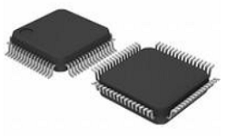
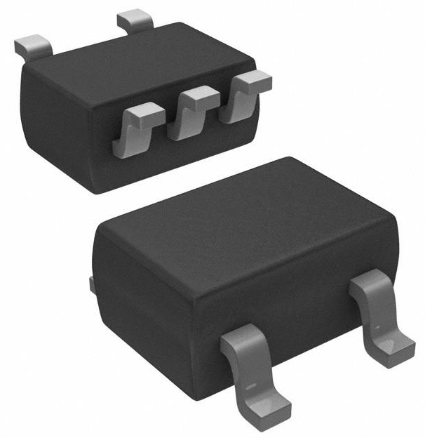
LT3750 Package

LT3750 Package
LT3750 Manufacturer
As a member of the S&P 500, Linear Technology Corporation is committed to designing, manufacturing and marketing an extensive line of high-performance analogue integrated circuits for main companies around the world. Between the analogue world and digital electronic products in communications, networks, industry, automobiles, computers, medical, instrumentation, consumer, military and aerospace systems, our products have built an important bridge for them. Our products include not only the production of power management, data conversion, signal conditioning, RF and interface ICs, μModule subsystems, but also wireless sensor network products.
Datasheet PDF
- Datasheets :
- PCN Design/Specification :
- Design Resources :
- Simulation Models :
Trend Analysis"
Is LT3750 a capacitor charger controller?
Yes, The LT® 3750 is a flyback converter designed to rapidly charge large capacitors to a user-adjustable target voltage. A patented boundary mode control scheme* minimizes transition losses and reduces transformer size. LT3750 can operate from a variety of power sources. A typical application can charge a 100µF capacitor to 300V in less than 300ms.
How do the pins of LT3750 work?
The CHARGE pin gives full control of the LT3750 to the user. The DONE pin indicates when the capacitor has reached its programmed value and the part has stopped charging.
What package is the LT3750 available in?
It is available in 10-Lead MS Package.
 P5010 vs. P5020: What is the Difference
23 July 2021335
 STM32L431RCT6 Microcontroller: Features, Applications and Datasheet
13 November 20232335
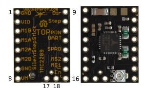 How to Interface TMC2209 Stepper Driver with Microcontroller?
26 November 202120988
 TP4056 Standalone Linear Li-Lon Battery Charger: Datasheet, Schematics and Current
18 October 202129771
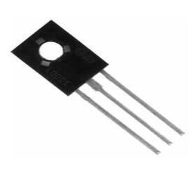 BD237: 3MHz,350mW, Pinout and Datasheet
15 April 2022449
 SS430 Sensor Module: Datasheet, Application, Benefits
12 August 2021642
 AT90CAN12815MT: Technical Product Analysis
29 February 2024127
 SN74LVC1G14DCKR: Overview, Features, and Applications
13 December 2023606
 Characteristics and Working Principle of IGBT
31 October 202519357
 What is an Electromagnetic Relay?
13 October 20209723
 Arm's IPO: A New Chapter in Chip Technology
30 August 20232132
 Dismantling and Analyzing Each Component in the Switching Power Supply
16 February 20226442
 16 Q&A About the Secrets of Operational Amplifiers
27 March 20254418
 Why Precision Matters in Analog-to-Digital Conversion
28 May 2025582
 Volkswagen CFO: Chip Supply Shortage Will Continue Until 2024
11 April 20223370
 Everything You Need to Know about RF Chip
14 January 202616956
Linear Technology/Analog Devices
In Stock
Minimum: 1 Multiples: 1
Qty
Unit Price
Ext Price
1
$4.988936
$4.99
10
$4.706544
$47.07
100
$4.440136
$444.01
500
$4.188807
$2,094.40
1000
$3.951705
$3,951.70
Not the price you want? Send RFQ Now and we'll contact you ASAP.
Inquire for More Quantity
![AD8232ACPZ-R7]() AD8232ACPZ-R7
AD8232ACPZ-R7Analog Devices Inc.
![AD5560JSVUZ]() AD5560JSVUZ
AD5560JSVUZAnalog Devices Inc.
![AD9963BCPZ]() AD9963BCPZ
AD9963BCPZAnalog Devices Inc.
![AD5522JSVDZ]() AD5522JSVDZ
AD5522JSVDZAnalog Devices Inc.
![AD8233ACBZ-R7]() AD8233ACBZ-R7
AD8233ACBZ-R7Analog Devices Inc.
![AD9963BCPZRL]() AD9963BCPZRL
AD9963BCPZRLAnalog Devices Inc.
![AD5560JSVUZ-REEL]() AD5560JSVUZ-REEL
AD5560JSVUZ-REELAnalog Devices Inc.
![AD8452ASTZ]() AD8452ASTZ
AD8452ASTZAnalog Devices Inc.
![AD5522JSVUZ]() AD5522JSVUZ
AD5522JSVUZAnalog Devices Inc.
![AD5522JSVUZ-RL]() AD5522JSVUZ-RL
AD5522JSVUZ-RLAnalog Devices Inc.


