
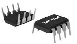
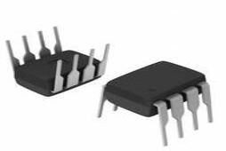
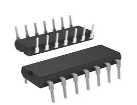
TL061 Operational Amplifier: Features, Pinout and Datasheet PDF

1 Channels 20mA per Channel 30pA 70 dB Instrumentational OP Amps 18V 6V~36V ±3V~18V TL061 8 Pins 8-SOIC (0.154, 3.90mm Width)


1 Channels 20mA per Channel 30pA 70 dB Instrumentational OP Amps 18V 6V~36V ±3V~18V TL061 8 Pins 8-SOIC (0.154, 3.90mm Width)
TL061 is a Low power JFET single operational amplifiers. This article mainly introduce its features, pinout, datasheet PDF and other detailed information about STMicroelectronics TL061

TL061 op amp alternating square wave generator prototype circuit powered by UA741 741 rail splitter
TL061 Description
The TL061 is a high-speed JFET-input single operational amplifier, which integrates well-matched high-voltage JFET and bipolar transistors in a monolithic integrated circuit. The device has a high slew rate, low input bias and offset current, and low offset voltage temperature coefficient.
TL061 Pinout

TL061 CAD Model
Symbol

Footprint

3D Model

TL061 Features
■ Very low power consumption: 200 µA
■ Wide common mode (up to VCC+) and Differential voltage range
■ Low input bias and offset current
■ Output short circuit protection
■ High input impedance JFET input stage
■ Internal frequency compensation
■ Latch-free operation
■ High slew rate: 3.5 V/µs
Specifications
- TypeParameter
- Mount
In electronic components, the term "Mount" typically refers to the method or process of physically attaching or fixing a component onto a circuit board or other electronic device. This can involve soldering, adhesive bonding, or other techniques to secure the component in place. The mounting process is crucial for ensuring proper electrical connections and mechanical stability within the electronic system. Different components may have specific mounting requirements based on their size, shape, and function, and manufacturers provide guidelines for proper mounting procedures to ensure optimal performance and reliability of the electronic device.
Surface Mount - Mounting Type
The "Mounting Type" in electronic components refers to the method used to attach or connect a component to a circuit board or other substrate, such as through-hole, surface-mount, or panel mount.
Surface Mount - Package / Case
refers to the protective housing that encases an electronic component, providing mechanical support, electrical connections, and thermal management.
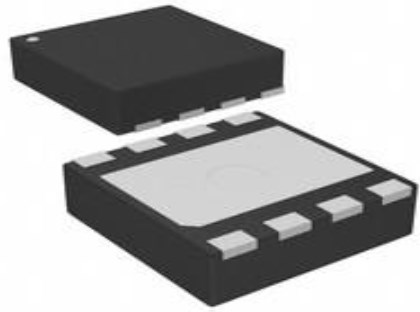
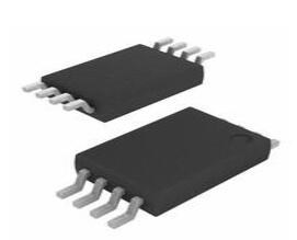
8-SOIC (0.154, 3.90mm Width) - Number of Pins8
- Operating Temperature
The operating temperature is the range of ambient temperature within which a power supply, or any other electrical equipment, operate in. This ranges from a minimum operating temperature, to a peak or maximum operating temperature, outside which, the power supply may fail.
0°C~70°C - Packaging
Semiconductor package is a carrier / shell used to contain and cover one or more semiconductor components or integrated circuits. The material of the shell can be metal, plastic, glass or ceramic.
Tube - JESD-609 Code
The "JESD-609 Code" in electronic components refers to a standardized marking code that indicates the lead-free solder composition and finish of electronic components for compliance with environmental regulations.
e4 - Part Status
Parts can have many statuses as they progress through the configuration, analysis, review, and approval stages.
Obsolete - Moisture Sensitivity Level (MSL)
Moisture Sensitivity Level (MSL) is a standardized rating that indicates the susceptibility of electronic components, particularly semiconductors, to moisture-induced damage during storage and the soldering process, defining the allowable exposure time to ambient conditions before they require special handling or baking to prevent failures
1 (Unlimited) - Number of Terminations8
- ECCN Code
An ECCN (Export Control Classification Number) is an alphanumeric code used by the U.S. Bureau of Industry and Security to identify and categorize electronic components and other dual-use items that may require an export license based on their technical characteristics and potential for military use.
EAR99 - Terminal Finish
Terminal Finish refers to the surface treatment applied to the terminals or leads of electronic components to enhance their performance and longevity. It can improve solderability, corrosion resistance, and overall reliability of the connection in electronic assemblies. Common finishes include nickel, gold, and tin, each possessing distinct properties suitable for various applications. The choice of terminal finish can significantly impact the durability and effectiveness of electronic devices.
Nickel/Palladium/Gold (Ni/Pd/Au) - Terminal Position
In electronic components, the term "Terminal Position" refers to the physical location of the connection points on the component where external electrical connections can be made. These connection points, known as terminals, are typically used to attach wires, leads, or other components to the main body of the electronic component. The terminal position is important for ensuring proper connectivity and functionality of the component within a circuit. It is often specified in technical datasheets or component specifications to help designers and engineers understand how to properly integrate the component into their circuit designs.
DUAL - Terminal Form
Occurring at or forming the end of a series, succession, or the like; closing; concluding.
GULL WING - Peak Reflow Temperature (Cel)
Peak Reflow Temperature (Cel) is a parameter that specifies the maximum temperature at which an electronic component can be exposed during the reflow soldering process. Reflow soldering is a common method used to attach electronic components to a circuit board. The Peak Reflow Temperature is crucial because it ensures that the component is not damaged or degraded during the soldering process. Exceeding the specified Peak Reflow Temperature can lead to issues such as component failure, reduced performance, or even permanent damage to the component. It is important for manufacturers and assemblers to adhere to the recommended Peak Reflow Temperature to ensure the reliability and functionality of the electronic components.
260 - Number of Functions1
- Supply Voltage
Supply voltage refers to the electrical potential difference provided to an electronic component or circuit. It is crucial for the proper operation of devices, as it powers their functions and determines performance characteristics. The supply voltage must be within specified limits to ensure reliability and prevent damage to components. Different electronic devices have specific supply voltage requirements, which can vary widely depending on their design and intended application.
15V - Time@Peak Reflow Temperature-Max (s)
Time@Peak Reflow Temperature-Max (s) refers to the maximum duration that an electronic component can be exposed to the peak reflow temperature during the soldering process, which is crucial for ensuring reliable solder joint formation without damaging the component.
30 - Base Part Number
The "Base Part Number" (BPN) in electronic components serves a similar purpose to the "Base Product Number." It refers to the primary identifier for a component that captures the essential characteristics shared by a group of similar components. The BPN provides a fundamental way to reference a family or series of components without specifying all the variations and specific details.
TL061 - Pin Count
a count of all of the component leads (or pins)
8 - Operating Supply Voltage
The voltage level by which an electrical system is designated and to which certain operating characteristics of the system are related.
18V - Number of Channels1
- Operating Supply Current
Operating Supply Current, also known as supply current or quiescent current, is a crucial parameter in electronic components that indicates the amount of current required for the device to operate under normal conditions. It represents the current drawn by the component from the power supply while it is functioning. This parameter is important for determining the power consumption of the component and is typically specified in datasheets to help designers calculate the overall power requirements of their circuits. Understanding the operating supply current is essential for ensuring proper functionality and efficiency of electronic systems.
200μA - Nominal Supply Current
Nominal current is the same as the rated current. It is the current drawn by the motor while delivering rated mechanical output at its shaft.
250μA - Power Dissipation
the process by which an electronic or electrical device produces heat (energy loss or waste) as an undesirable derivative of its primary action.
680mW - Slew Rate
the maximum rate of output voltage change per unit time.
3.5V/μs - Architecture
In electronic components, the parameter "Architecture" refers to the overall design and structure of the component. It encompasses the arrangement of internal components, the layout of circuitry, and the physical form of the component. The architecture of an electronic component plays a crucial role in determining its functionality, performance, and compatibility with other components in a system. Different architectures can result in variations in power consumption, speed, size, and other key characteristics of the component. Designers often consider the architecture of electronic components carefully to ensure optimal performance and integration within a larger system.
VOLTAGE-FEEDBACK - Amplifier Type
Amplifier Type refers to the classification or categorization of amplifiers based on their design, functionality, and characteristics. Amplifiers are electronic devices that increase the amplitude of a signal, such as voltage or current. The type of amplifier determines its specific application, performance capabilities, and operating characteristics. Common types of amplifiers include operational amplifiers (op-amps), power amplifiers, audio amplifiers, and radio frequency (RF) amplifiers. Understanding the amplifier type is crucial for selecting the right component for a particular circuit or system design.
J-FET - Common Mode Rejection Ratio
Common Mode Rejection Ratio (CMRR) is a measure of the ability of a differential amplifier to reject input signals that are common to both input terminals. It is defined as the ratio of the differential gain to the common mode gain. A high CMRR indicates that the amplifier can effectively eliminate noise and interference that affects both inputs simultaneously, enhancing the fidelity of the amplified signal. CMRR is typically expressed in decibels (dB), with higher values representing better performance in rejecting common mode signals.
70 dB - Current - Input Bias
The parameter "Current - Input Bias" in electronic components refers to the amount of current required at the input terminal of a device to maintain proper operation. It is a crucial specification as it determines the minimum input current needed for the component to function correctly. Input bias current can affect the performance and accuracy of the device, especially in precision applications where small signal levels are involved. It is typically specified in datasheets for operational amplifiers, transistors, and other semiconductor devices to provide users with important information for circuit design and analysis.
30pA - Voltage - Supply, Single/Dual (±)
The parameter "Voltage - Supply, Single/Dual (±)" in electronic components refers to the power supply voltage required for the proper operation of the component. This parameter indicates whether the component requires a single power supply voltage (e.g., 5V) or a dual power supply voltage (e.g., ±15V). For components that require a single power supply voltage, only one voltage level is needed for operation. On the other hand, components that require a dual power supply voltage need both positive and negative voltage levels to function correctly.Understanding the voltage supply requirements of electronic components is crucial for designing and integrating them into circuits to ensure proper functionality and prevent damage due to incorrect voltage levels.
6V~36V ±3V~18V - Output Current per Channel
Output Current per Channel is a specification commonly found in electronic components such as amplifiers, audio interfaces, and power supplies. It refers to the maximum amount of electrical current that can be delivered by each individual output channel of the component. This parameter is important because it determines the capacity of the component to drive connected devices or loads. A higher output current per channel means the component can deliver more power to connected devices, while a lower output current may limit the performance or functionality of the component in certain applications. It is crucial to consider the output current per channel when selecting electronic components to ensure they can meet the power requirements of the intended system or setup.
20mA - Input Offset Voltage (Vos)
Input Offset Voltage (Vos) is a key parameter in electronic components, particularly in operational amplifiers. It refers to the voltage difference that must be applied between the two input terminals of the amplifier to nullify the output voltage when the input terminals are shorted together. In simpler terms, it represents the voltage required to bring the output of the amplifier to zero when there is no input signal present. Vos is an important parameter as it can introduce errors in the output signal of the amplifier, especially in precision applications where accuracy is crucial. Minimizing Vos is essential to ensure the amplifier operates with high precision and accuracy.
15mV - Neg Supply Voltage-Nom (Vsup)
The parameter "Neg Supply Voltage-Nom (Vsup)" in electronic components refers to the nominal negative supply voltage that the component requires to operate within its specified performance characteristics. This parameter indicates the minimum voltage level that must be provided to the component's negative supply pin for proper functionality. It is important to ensure that the negative supply voltage provided to the component does not exceed the maximum specified value to prevent damage or malfunction. Understanding and adhering to the specified negative supply voltage requirements is crucial for the reliable operation of the electronic component in a circuit.
-15V - Unity Gain BW-Nom
Unity Gain Bandwidth, often abbreviated as Unity Gain BW or UGBW, refers to the frequency at which an amplifier can provide a gain of one (0 dB). It is a critical parameter in assessing the performance of operational amplifiers and other amplifying devices, indicating the range of frequencies over which the amplifier can operate without distortion. Unity Gain BW is particularly important in applications where signal fidelity is crucial, as it helps determine the maximum frequency of operation for a given gain level. As the gain is reduced, the bandwidth typically increases, ensuring that the amplifier can still operate effectively across various signal frequencies.
1000 kHz - Voltage Gain
Voltage gain is a measure of how much an electronic component or circuit amplifies an input voltage signal to produce an output voltage signal. It is typically expressed as a ratio or in decibels (dB). A higher voltage gain indicates a greater amplification of the input signal. Voltage gain is an important parameter in amplifiers, where it determines the level of amplification provided by the circuit. It is calculated by dividing the output voltage by the input voltage and is a key factor in determining the overall performance and functionality of electronic devices.
75.56dB - Low-Offset
Low-offset is a parameter used to describe the level of offset voltage in electronic components, particularly in operational amplifiers. Offset voltage refers to the small voltage difference that exists between the input terminals of the amplifier when the input voltage is zero. A low-offset value indicates that this voltage difference is minimal, which is desirable for accurate signal processing and amplification. Components with low-offset specifications are preferred in applications where precision and accuracy are critical, such as in instrumentation and measurement systems. Minimizing offset voltage helps reduce errors and ensures the faithful reproduction of input signals by the amplifier.
NO - Frequency Compensation
Frequency compensation is implemented by modifying the gain and phase characteristics of the amplifier's open loop output or of its feedback network, or both, in such a way as to avoid the conditions leading to oscillation. This is usually done by the internal or external use of resistance-capacitance networks.
YES - Voltage - Input Offset
Voltage - Input Offset is a parameter that refers to the difference in voltage between the input terminals of an electronic component, such as an operational amplifier, when the input voltage is zero. It is an important characteristic that can affect the accuracy and performance of the component in various applications. A low input offset voltage is desirable as it indicates that the component will have minimal error in its output when the input signal is near zero. Manufacturers typically provide this specification in the component's datasheet to help users understand the component's behavior and make informed decisions when designing circuits.
3mV - Low-Bias
Low-bias in electronic components refers to a design or configuration that minimizes the amount of bias current flowing through the component. Bias current is a small, steady current that is used to establish the operating point of a component, such as a transistor or amplifier. By reducing the bias current to a low level, the component can operate with lower power consumption and potentially lower distortion. Low-bias components are often used in applications where power efficiency and signal fidelity are important, such as in audio amplifiers or battery-powered devices. Overall, the low-bias parameter indicates the ability of the component to operate efficiently and accurately with minimal bias current.
YES - Bias Current-Max (IIB) @25C
The parameter "Bias Current-Max (IIB) @25C" in electronic components refers to the maximum input bias current that the component can handle at a specified temperature of 25 degrees Celsius. Bias current is the current flowing into the input terminal of a device when no signal is applied. This parameter is important because excessive bias current can affect the performance and stability of the component, leading to potential issues such as distortion or offset errors in the output signal. By specifying the maximum bias current allowed at a certain temperature, manufacturers provide users with important information to ensure proper operation and reliability of the component in their circuit designs.
0.0004μA - Dual Supply Voltage
Dual Supply Voltage refers to an electronic component's requirement for two separate power supply voltages, typically one positive and one negative. This configuration is commonly used in operational amplifiers, analog circuits, and certain digital devices to allow for greater signal handling capabilities and improved performance. The use of dual supply voltages enables the device to process bipolar signals, thereby enhancing its functionality in various applications.
9V - Input Offset Current-Max (IIO)
Input Offset Current-Max (IIO) is a parameter that describes the maximum difference in input bias currents between two input terminals of an electronic component, such as an operational amplifier. Input offset current can cause errors in the output of the component, especially in precision applications where accuracy is crucial. The IIO specification provides a limit on the maximum allowable difference in input currents to ensure that the component operates within its specified performance range. Designers need to consider the IIO value when selecting components and designing circuits to minimize errors and ensure reliable operation.
0.005μA - Height1.25mm
- Length4.9mm
- Width3.9mm
- REACH SVHC
The parameter "REACH SVHC" in electronic components refers to the compliance with the Registration, Evaluation, Authorization, and Restriction of Chemicals (REACH) regulation regarding Substances of Very High Concern (SVHC). SVHCs are substances that may have serious effects on human health or the environment, and their use is regulated under REACH to ensure their safe handling and minimize their impact.Manufacturers of electronic components need to declare if their products contain any SVHCs above a certain threshold concentration and provide information on the safe use of these substances. This information allows customers to make informed decisions about the potential risks associated with using the components and take appropriate measures to mitigate any hazards.Ensuring compliance with REACH SVHC requirements is essential for electronics manufacturers to meet regulatory standards, protect human health and the environment, and maintain transparency in their supply chain. It also demonstrates a commitment to sustainability and responsible manufacturing practices in the electronics industry.
No SVHC - Radiation Hardening
Radiation hardening is the process of making electronic components and circuits resistant to damage or malfunction caused by high levels of ionizing radiation, especially for environments in outer space (especially beyond the low Earth orbit), around nuclear reactors and particle accelerators, or during nuclear accidents or nuclear warfare.
No - RoHS Status
RoHS means “Restriction of Certain Hazardous Substances” in the “Hazardous Substances Directive” in electrical and electronic equipment.
ROHS3 Compliant - Lead Free
Lead Free is a term used to describe electronic components that do not contain lead as part of their composition. Lead is a toxic material that can have harmful effects on human health and the environment, so the electronics industry has been moving towards lead-free components to reduce these risks. Lead-free components are typically made using alternative materials such as silver, copper, and tin. Manufacturers must comply with regulations such as the Restriction of Hazardous Substances (RoHS) directive to ensure that their products are lead-free and environmentally friendly.
Lead Free
TL061 Applications
• Tablets
• Computers
• White goods
• Personal electronics
TL061 Functional Block Diagram

Functional Block Diagram

Input offset voltage null circuit
TL061 Schematic Diagram

TL061 Package Outline

TL061 Example Board Layout

TL061 Manufacturer
■STMicroelectronics is a French-Italian multinational electronics and semiconductor manufacturer headquartered in Geneva, Switzerland.
■It was formed by the merger of two state-owned semiconductor companies in 1987: France's "Thomson Semiconducteurs" and Italy's "SGS Microelettronica".
■It is often referred to as "ST" and is the largest semiconductor chip manufacturer in Europe by revenue.
■STMicroelectronics corporate headquarters and EMEA regional headquarters are located in Geneva, while the holding company STMicroelectronics N.V. is incorporated in the Netherlands.
■The company's US headquarters are located in Koper, Texas. The Asia-Pacific region is headquartered in Singapore, while the Japan and South Korea operations are headquartered in Tokyo. The headquarter of the company in China is located in Shanghai.
Trend Analysis
Datasheet PDF
- Datasheets :
1.What op amps can replace IF356?
You can use TL031, TL061, and TL071, which are single op amps with high input impedance and pin compatible.
2.I need an op amp to be used as a voltage follower to follow a voltage of 2-12V, but the following voltage has no drive capability. What op amp is suitable?
If you only need higher input impedance of the op amp, you can use TL031, TL051, TL061, and LF411. If not only the input impedance is high, but also the drive capability is higher, it is recommended that you use TLE2072, TLE2082. The output current of each model can reach ±80mA.
3.Is there a single op amp that can replace OP37?
TL061 can replace it.
4.Is TL061 a single operational amplifier or a dual operational amplifier?
It is a single operational amplifier.
 TPS54061DRBT, 60V, Step-Down, MOSFETs, 200mA
24 February 2022238
![SIM800L How to use SIM800L GSM Module with Arduino?[Video]](https://res.utmel.com/Images/Article/37707472-93f2-4011-a845-027095acee4e.png) SIM800L How to use SIM800L GSM Module with Arduino?[Video]
SIM800L How to use SIM800L GSM Module with Arduino?[Video]23 September 20239736
 CA3140E Circuit - 8-PDIP IC OPAMP GP 1:Datasheet, Circuit, Pinout, and Equivalents
18 February 2022750
 LM2574 0.5A Buck Regulator: Datasheet pdf, Pinout and Circuit
09 December 20211325
 TS555 CMOS Timer: Datasheet, Application, Schematic
24 September 20212329
![How to Use MJE15032?[FAQ]](https://res.utmel.com/Images/Article/74d9fd02-3e3b-42ad-9486-60adc9fa5d4c.jpg) How to Use MJE15032?[FAQ]
How to Use MJE15032?[FAQ]14 April 20222308
 LM2900 Operational Amplifier: Datasheet, Equivalent, Pinout
11 October 20211886
 Exploring the STM32F410CBT6 Microcontroller: Features, Specifications, and Applications
29 February 2024123
 Hall Effect: Definition, Principle, Measurement Methods
08 November 20228469
 Why Meta Did Not Choose Qualcomm AI Chip?
02 April 20224097
 The Introduction of Car Fuse
09 October 20214617
 0 Ohm Resistor Explained
10 December 202115484
 What is IMU: Definition, Features and Prospects
12 April 20223845
 What is a Fixed Inductor?
15 April 202111065
 STMicroelectronics: The European Powerhouse in Silicon Carbide Semiconductor Technology
05 October 20231688
 A Study of the Interelectrode Capacitances of SiC and GaN Power Semiconductor Devices Using Multiple Current Probes
01 February 20231032
STMicroelectronics
In Stock: 6000
United States
China
Canada
Japan
Russia
Germany
United Kingdom
Singapore
Italy
Hong Kong(China)
Taiwan(China)
France
Korea
Mexico
Netherlands
Malaysia
Austria
Spain
Switzerland
Poland
Thailand
Vietnam
India
United Arab Emirates
Afghanistan
Åland Islands
Albania
Algeria
American Samoa
Andorra
Angola
Anguilla
Antigua & Barbuda
Argentina
Armenia
Aruba
Australia
Azerbaijan
Bahamas
Bahrain
Bangladesh
Barbados
Belarus
Belgium
Belize
Benin
Bermuda
Bhutan
Bolivia
Bonaire, Sint Eustatius and Saba
Bosnia & Herzegovina
Botswana
Brazil
British Indian Ocean Territory
British Virgin Islands
Brunei
Bulgaria
Burkina Faso
Burundi
Cabo Verde
Cambodia
Cameroon
Cayman Islands
Central African Republic
Chad
Chile
Christmas Island
Cocos (Keeling) Islands
Colombia
Comoros
Congo
Congo (DRC)
Cook Islands
Costa Rica
Côte d’Ivoire
Croatia
Cuba
Curaçao
Cyprus
Czechia
Denmark
Djibouti
Dominica
Dominican Republic
Ecuador
Egypt
El Salvador
Equatorial Guinea
Eritrea
Estonia
Eswatini
Ethiopia
Falkland Islands
Faroe Islands
Fiji
Finland
French Guiana
French Polynesia
Gabon
Gambia
Georgia
Ghana
Gibraltar
Greece
Greenland
Grenada
Guadeloupe
Guam
Guatemala
Guernsey
Guinea
Guinea-Bissau
Guyana
Haiti
Honduras
Hungary
Iceland
Indonesia
Iran
Iraq
Ireland
Isle of Man
Israel
Jamaica
Jersey
Jordan
Kazakhstan
Kenya
Kiribati
Kosovo
Kuwait
Kyrgyzstan
Laos
Latvia
Lebanon
Lesotho
Liberia
Libya
Liechtenstein
Lithuania
Luxembourg
Macao(China)
Madagascar
Malawi
Maldives
Mali
Malta
Marshall Islands
Martinique
Mauritania
Mauritius
Mayotte
Micronesia
Moldova
Monaco
Mongolia
Montenegro
Montserrat
Morocco
Mozambique
Myanmar
Namibia
Nauru
Nepal
New Caledonia
New Zealand
Nicaragua
Niger
Nigeria
Niue
Norfolk Island
North Korea
North Macedonia
Northern Mariana Islands
Norway
Oman
Pakistan
Palau
Palestinian Authority
Panama
Papua New Guinea
Paraguay
Peru
Philippines
Pitcairn Islands
Portugal
Puerto Rico
Qatar
Réunion
Romania
Rwanda
Samoa
San Marino
São Tomé & Príncipe
Saudi Arabia
Senegal
Serbia
Seychelles
Sierra Leone
Sint Maarten
Slovakia
Slovenia
Solomon Islands
Somalia
South Africa
South Sudan
Sri Lanka
St Helena, Ascension, Tristan da Cunha
St. Barthélemy
St. Kitts & Nevis
St. Lucia
St. Martin
St. Pierre & Miquelon
St. Vincent & Grenadines
Sudan
Suriname
Svalbard & Jan Mayen
Sweden
Syria
Tajikistan
Tanzania
Timor-Leste
Togo
Tokelau
Tonga
Trinidad & Tobago
Tunisia
Turkey
Turkmenistan
Turks & Caicos Islands
Tuvalu
U.S. Outlying Islands
U.S. Virgin Islands
Uganda
Ukraine
Uruguay
Uzbekistan
Vanuatu
Vatican City
Venezuela
Wallis & Futuna
Yemen
Zambia
Zimbabwe


