

 Product
 Brand
Brand Articles
 Tools
Tools
ADC Selection Guide: Architectures, Resolution, Sample Rate, and Digital Interfaces
This technical selection guide provides hardware engineers and analog system designers with a mathematical and architectural framework for selecting analog-to-digital converters (ADCs). Matching an ADC to a specific mixed-signal application requires evaluating converter topologies, dynamic noise metrics, switched-capacitor input settling dynamics, clock jitter limits, reference drift budgets, and digital interface throughput.
Selecting an ADC based strictly on nominal resolution and maximum sampling speed frequently results in compromised bench performance. A nominal 16-bit converter can easily degrade to 11 Effective Number of Bits (ENOB) if front-end drive settling, reference noise, or clock phase noise are improperly budgeted. This guide details the mathematical equations, circuit models, and interface criteria required to optimize ADC selection across Successive Approximation Register (SAR), Delta-Sigma (ΔΣ), and Pipelined topologies.
ADC Architecture Taxonomy and Selection Criteria
ADC architecture selection depends on signal bandwidth, conversion latency, channel count, and dynamic range requirements.
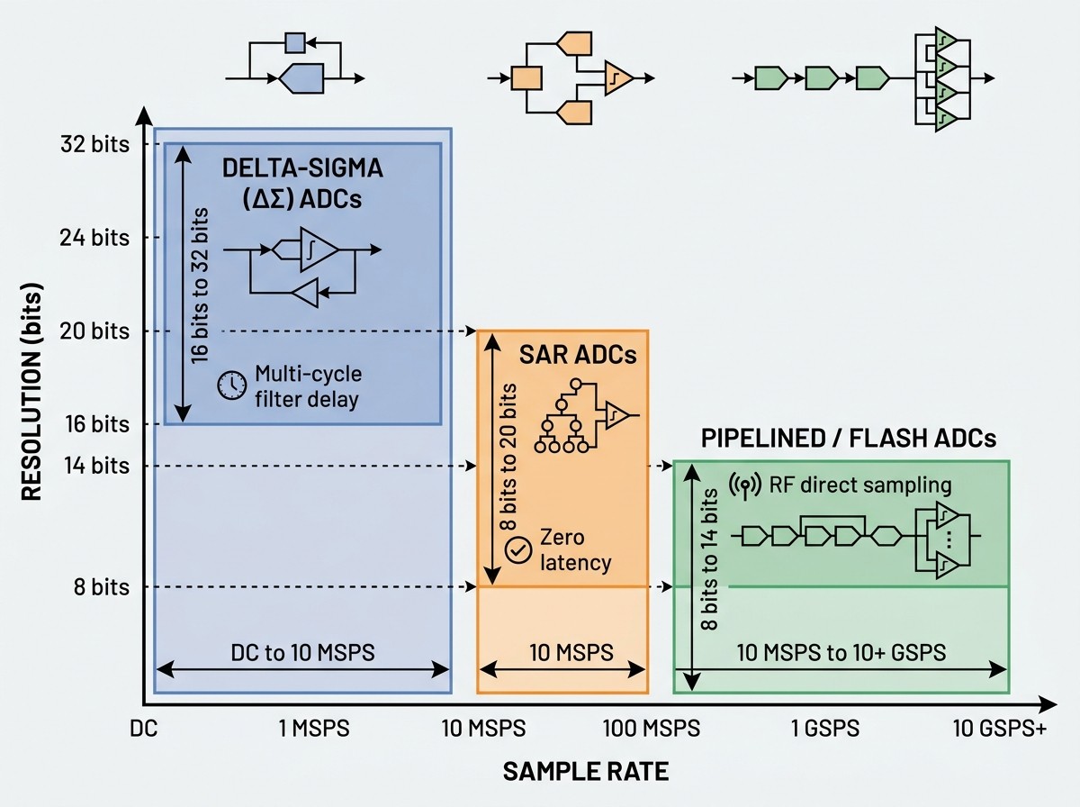
Successive Approximation Register ADCs for Low-Latency and Multiplexed Systems
Successive Approximation Register (SAR) ADCs execute a binary search algorithm using an internal capacitive digital-to-analog converter (CDAC) and comparator network. The conversion cycle completes within a fixed number of clock cycles (typically N cycles for an N-bit converter).
SAR converters offer three core advantages:
Zero Latency: Conversion data is available at the end of the acquisition and conversion cycle without digital decimation delay. This makes SAR ADCs optimal for closed-loop control systems (such as motor drives and switch-mode power supplies) and rapid multi-channel multiplexing.
Power Scaling: Power consumption scales linearly with the sampling rate (fs), conserving energy in duty-cycled or low-throughput sensing nodes.
Resolution Envelope: Modern SAR architectures deliver resolutions from 8 to 20 bits at throughputs reaching 5 to 10 MSPS.
Delta-Sigma ADCs for High-Resolution DC and Precision Audio
Delta-Sigma (ΔΣ) converters combine oversampling, continuous- or discrete-time modulators, and active noise shaping to push quantization noise[8] outside the signal band of interest, followed by a digital decimation filter.
The key characteristics of Delta-Sigma architectures include:
Ultra-High Dynamic Range: Achieving 16-bit to 32-bit resolution across bandwidths ranging from DC to a few megahertz.
Relaxed Anti-Aliasing Requirements: Because the effective sampling rate occurs at the oversampled modulator clock (fmod = OSR · fs), the Nyquist zone is shifted higher in frequency, allowing simple first- or second-order passive RC anti-aliasing filters.
Conversion Latency: The internal digital filter (typically sinc or FIR topologies) introduces multi-cycle group delay. This latency makes Delta-Sigma ADCs less suitable for fast multiplexed inputs or real-time closed-loop feedback paths unless specialized low-latency/sinc3 filters are employed.
Pipelined and Flash ADCs for High-Speed Communications and Radar
Pipelined ADCs divide the quantization process into multiple consecutive stages. Each stage consists of a low-resolution sub-ADC (Flash converter), a sub-DAC, a subtractor to calculate the residue voltage, and a residue amplifier that passes the amplified error to the subsequent stage with digital error correction.
Throughput Envelope: Pipelined converters operate from 10 MSPS to several GSPS with bit depths typically spanning 8 to 14 bits. Pure Flash converters scale beyond 10 GSPS at lower resolutions (6 to 8 bits).
Direct RF and IF Sampling: These converters dominate wideband software-defined radios (SDR), phased-array radar, intermediate-frequency (IF) digitizers, and high-speed oscilloscopes.
Latency Profile: Unlike SAR ADCs, Pipelined ADCs exhibit a data pipeline latency proportional to the number of stages (typically 5 to 15 clock cycles), though a new data word is output on every clock edge once the pipeline is full.
ADC Architecture Comparison Matrix
| Architecture | Nominal Resolution | Max Sample Rate (fs) | Conversion Latency | Multiplexing Suitability | Anti-Aliasing Filter Order | Dominant Applications |
|---|---|---|---|---|---|---|
| SAR | 8 to 20 Bits | Up to 10 MSPS | Zero (Single-cycle) | Excellent | Moderate (2nd to 4th order) | Industrial control, motor drives, multiplexed DAQs, battery monitors |
| Delta-Sigma (ΔΣ) | 16 to 32 Bits | DC to ~10 MSPS | High (Multi-cycle group delay) | Poor to Fair (Requires settling time) | Low (1st or 2nd order passive) | Weigh scales, strain gauges, audio processing, seismic sensing, precision DC |
| Pipelined | 8 to 14 Bits | 10 MSPS to 5 GSPS | Moderate (Pipeline stages) | Moderate | High (Steep analog filter required) | Cellular base stations, SDR receivers, radar, wideband test equipment |
| Flash | 6 to 8 Bits | > 10 GSPS | Ultra-Low (< 2 cycles) | Poor | Very High | Ultra-wideband optical receivers, direct RF sampling front-ends |
Resolution, Dynamic Range, and Real-World Signal Metrics
ADC dynamic range and resolution are governed by quantization noise, wideband thermal noise (kT/C), and non-linear harmonic distortion.
Nominal Resolution vs. Effective Number of Bits
According to IEEE Standard 1241-2010 and established converter theory, the theoretical Signal-to-Noise Ratio (SNR) for an ideal N-bit converter[1] sampled across the full Nyquist bandwidth is:
SNRideal = 6.02 · N + 1.76 dB
Real-world converters do not achieve this theoretical limit because wideband thermal noise, reference noise, and integrated distortion reduce dynamic performance. To quantify actual performance under specific operating conditions, convert the measured Signal-to-Noise and Distortion (SINAD) into the Effective Number of Bits (ENOB)[2]:
ENOB = (SINAD - 1.76 dB) / 6.02
When reviewing datasheets, evaluate ENOB at your system's actual input frequency (fin) and sample rate (fs). An ADC rated at 16-bit nominal resolution might provide 15.2 ENOB at DC, but degrade to 12.1 ENOB when sampling an input signal at fin = 2 MHz due to slew-rate limitations and internal clock phase noise.
Dynamic Specifications: SINAD, SNR, THD, and SFDR
Signal-to-Noise Ratio (SNR): The ratio of fundamental signal power to the integrated root-sum-square (RSS) noise power across the Nyquist bandwidth, explicitly excluding DC and harmonic components.
Total Harmonic Distortion (THD): The ratio of the fundamental signal power to the sum of the powers of its harmonic components (typically the 2nd through 6th harmonics):
THD = 10 log10((V22 + V32 + V42 + V52 + V62) / Vfund2)
Signal-to-Noise and Distortion (SINAD): The ratio of fundamental signal power to total noise power plus harmonic distortion power across the Nyquist band:
SINAD = -10 log10(10-SNR/10 + 10THD/10)
Spurious-Free Dynamic Range (SFDR): The usable dynamic range between the fundamental input signal and the peak spurious signal (whether harmonic or non-harmonic). In communications receivers, high SFDR prevents strong adjacent blockers from masking weak desired signals.
Static Linearity Specifications: DNL, INL, and Monotonicity
Static linearity specifications govern low-frequency and DC measurement precision:
Differential Non-Linearity (DNL): The deviation of an actual code step width from the ideal value of 1 LSB. If DNL < -1 LSB, code transitions can vanish, producing "missing codes." In closed-loop feedback loops, non-monotonicity or missing codes can induce control instability.
Integral Non-Linearity (INL): The maximum deviation of the actual transfer function from a straight line drawn through the end-points (End-Point INL) or calculated via linear regression (Best-Fit INL). INL directly causes non-linear DC transfer errors and cannot be calibrated out with simple offset and gain corrections.
Oversampling and Digital Processing Gain
Oversampling an input signal spreads the fixed quantization noise power (q2 / 12) over a wider Nyquist bandwidth (fs / 2). When the digitizer data is filtered and decimated back to the target signal bandwidth (fB), out-of-band noise is eliminated:
ΔSNR = 10 log10(OSR) = 10 log10(fs / (2 · fB))
For Nyquist-rate averaging, each 4× increase in the oversampling ratio (OSR = 4) yields +6.02 dB of SNR improvement, adding 1 bit of effective resolution.
In Delta-Sigma converters utilizing active noise shaping of order L, the SNR enhancement scales significantly faster:
ΔSNRΔΣ ≈ (6L + 3) dB per octave of oversampling
Pro Tip: While oversampling attenuates uncorrelated white quantization noise, it does not reduce coherent harmonic distortion or ADC integral non-linearity (INL). If INL dominates the converter error budget, oversampling alone will yield diminishing returns on dynamic range.
Analog Front-End Drive and Input Settling Calculations
An unbuffered switched-capacitor ADC front-end draws dynamic transient current pulses that must fully settle before conversion begins.
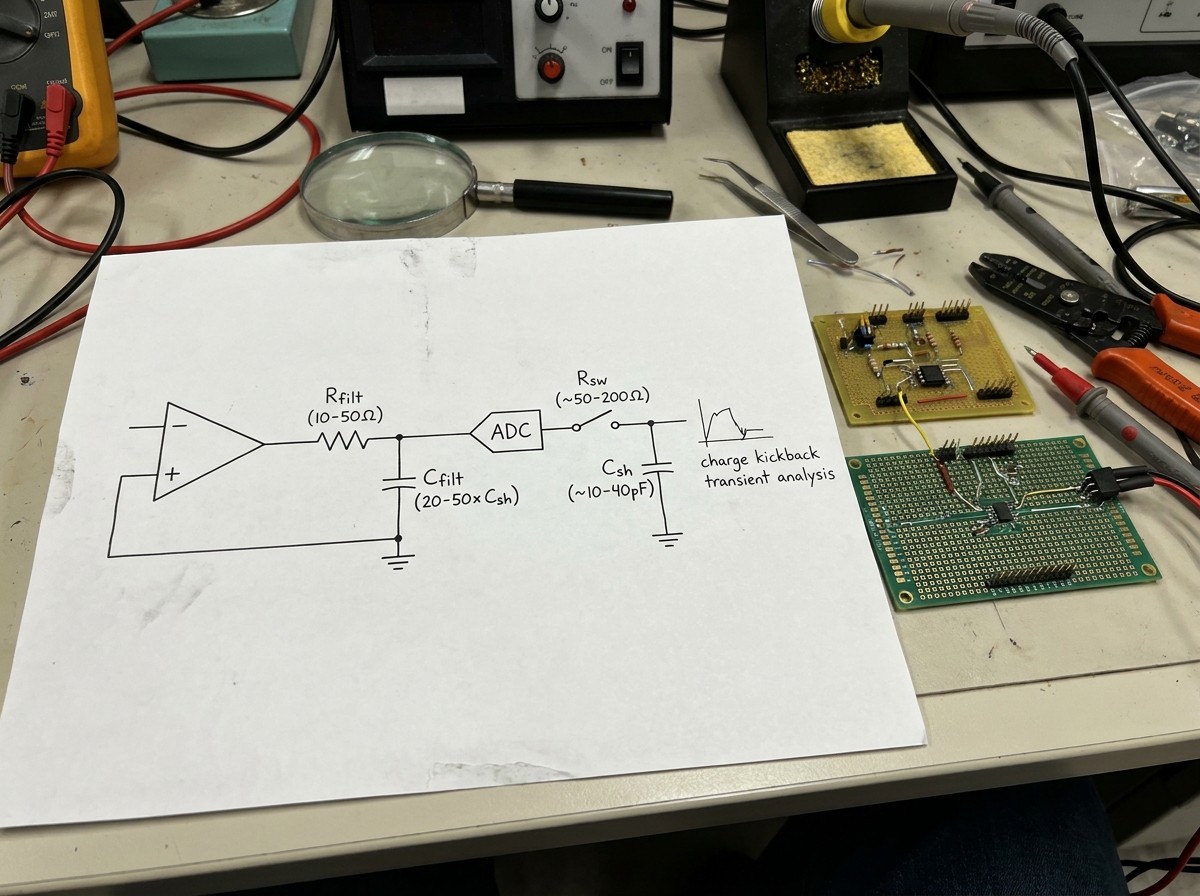
Switched-Capacitor Input Dynamics and Charge Kickback
Unbuffered SAR converters rely on a sampling capacitor (Csh, typically 10 pF to 40 pF) and an internal switch resistance (Rsw)[4], typically 50 Ω to 200 Ω. During the conversion phase, Csh is disconnected from the input.
When the converter transitions into the acquisition phase (tacq), the internal switch closes. The voltage mismatch between the external front-end driver and the residual charge on Csh triggers an instantaneous transient current draw, known as charge kickback.
Sizing the External RC Filter and Calculating Settling Time
To isolate the front-end amplifier and provide a reservoir of charge to absorb the kickback, place an external low-pass filter (Rfilt and Cfilt) directly at the ADC input pins.
Follow these sizing criteria:
Reservoir Capacitor Sizing: Size Cfilt such that it is 20 to 50 times larger than Csh:
Cfilt ≥ 20 · Csh
This attenuates the initial kickback voltage drop to less than 5% of the input signal step.
Settling Time Constant Formula: To achieve conversion accuracy to within 0.5 LSB of nominal resolution N, the input network must settle within the acquisition window (tacq)[5]:
tacq ≥ (N + 1) · ln(2) · τ ≈ (N + 1) × 0.693 · τ
where τ ≈ Rfilt · Cfilt.
Time Constant Multipliers:
For 16-bit accuracy: tacq ≥ 17 · ln(2) · τ ≈ 11.78τ
For 18-bit accuracy: tacq ≥ 19 · ln(2) · τ ≈ 13.16τ
ADC Driver Operational Amplifier Selection Criteria
The driving operational amplifier must possess sufficient bandwidth and phase margin to charge Cfilt without oscillating:
Gain-Bandwidth Product (GBW): Select an op-amp with a small-signal closed-loop bandwidth at least 3 to 4 times higher than the input RC filter cutoff frequency (f-3dB = 1 / (2π Rfilt Cfilt)).
Slew Rate (SR): Ensure the amplifier slews fast enough to follow the highest full-scale input frequency (fin) without distortion:
SR ≥ 2π · fin · Vpeak
Isolation Resistance: Never connect an operational amplifier output directly to Cfilt without a series isolation resistor (Rfilt). Sizing Rfilt between 10 Ω and 50 Ω isolates the amplifier from the capacitive load, preventing open-loop phase degradation and ringing.
Front-End RC Kickback Settling Calculation Workflow:
Extract Acquisition Window (tacq) and Csh from the ADC datasheet.
Select Filter Capacitor: Cfilt = 30 · Csh.
Compute Max Time Constant: τmax = tacq / ((N + 1) · ln(2)).
Calculate Series Resistor: Rfilt ≤ τmax / Cfilt.
Select Op-Amp: GBW ≥ 4 / (2π · Rfilt · Cfilt), SR ≥ 2π · fin · Vpeak.
Verify in SPICE: Ensure input transient settles to < 0.5 LSB within tacq.
Signal Chain Integrity: Clock Jitter, Voltage References, and Filtering
Sampling precision is bounded by sampling clock phase noise and voltage reference stability.
Aperture Jitter and High-Frequency SNR Degradation
Clock aperture jitter represents timing uncertainty (tj) in the sampling instant. When sampling an AC signal with a high slew rate (dV/dt), timing variations translate directly into amplitude noise.
The theoretical SNR degradation ceiling imposed by total timing jitter[3] (tj = √(tclk_jitter2 + taperture_jitter2)) is governed by:
SNRjitter = -20 log10(2π · fin · tj)
As documented in precision timing research on jitter versus SNR limits in ADCs[7], timing jitter becomes the dominant noise source at high input frequencies.
Practical Benchmark: Sampling an intermediate frequency signal of fin = 100 MHz using a clock source with 1 ps RMS jitter caps the theoretical SNR at:
SNRjitter = -20 log10(2π · 100 × 106 · 1 × 10-12) = 64.04 dB
This restricts dynamic performance to 10.35 ENOB, regardless of whether a 14-bit or 16-bit converter is specified in the design.
Voltage Reference Selection and DC Error Budgeting
The reference voltage (Vref) establishes the absolute scale of the ADC transfer function. Any drift, thermal noise, or load-regulation error on Vref scales full-scale gain error linearly:
ΔVout / Vout = ΔVref / Vref
Quantifying 1 LSB size as a fraction of full scale shows the precision requirements across bit depths:
16-bit converter: 1 LSB = 1 / 216 = 15.26 ppm
24-bit converter: 1 LSB = 1 / 224 = 0.0596 ppm
Consider a standard internal reference with a temperature coefficient of 10 ppm/°C. Across an industrial temperature rise of ΔT = 40°C, the reference drifts by 400 ppm:
In a 16-bit system, 400 ppm / 15.26 ppm = 26.2 LSBs of gain error.
In a 24-bit system, 400 ppm / 0.0596 ppm = 6,711.4 LSBs of error.
For high-resolution DC measurement systems, internal references are typically inadequate; specify an external low-drift reference (< 1 to 2 ppm/°C) paired with a dedicated reference buffer amplifier.
Anti-Aliasing Filter Design Trade-Offs
Sampling an analog signal folds all frequency components located above the Nyquist boundary (fs / 2) back into the baseband spectrum (|fin - k · fs|).
Nyquist-Rate ADCs (SAR / Pipelined): The transition band between the passband edge (fpass) and the stopband (fs - fpass) is narrow. Suppressing out-of-band signals and noise below the converter resolution floor requires 4th- to 8th-order active filtering topologies (such as Butterworth or Chebyshev alignments).
Oversampled Modulators (ΔΣ): The effective sampling rate is shifted to fmod = OSR · fs. The aliasing zone moves to fmod ± fB. Consequently, a first- or second-order passive RC filter at the input provides adequate roll-off, eliminating active filter distortion and noise contributions.
Digital Interface Selection: SPI, LVDS, and JESD204B/C
Digital interface selection is constrained by total throughput, board real estate, pin availability on host processors/FPGAs, and synchronization requirements.
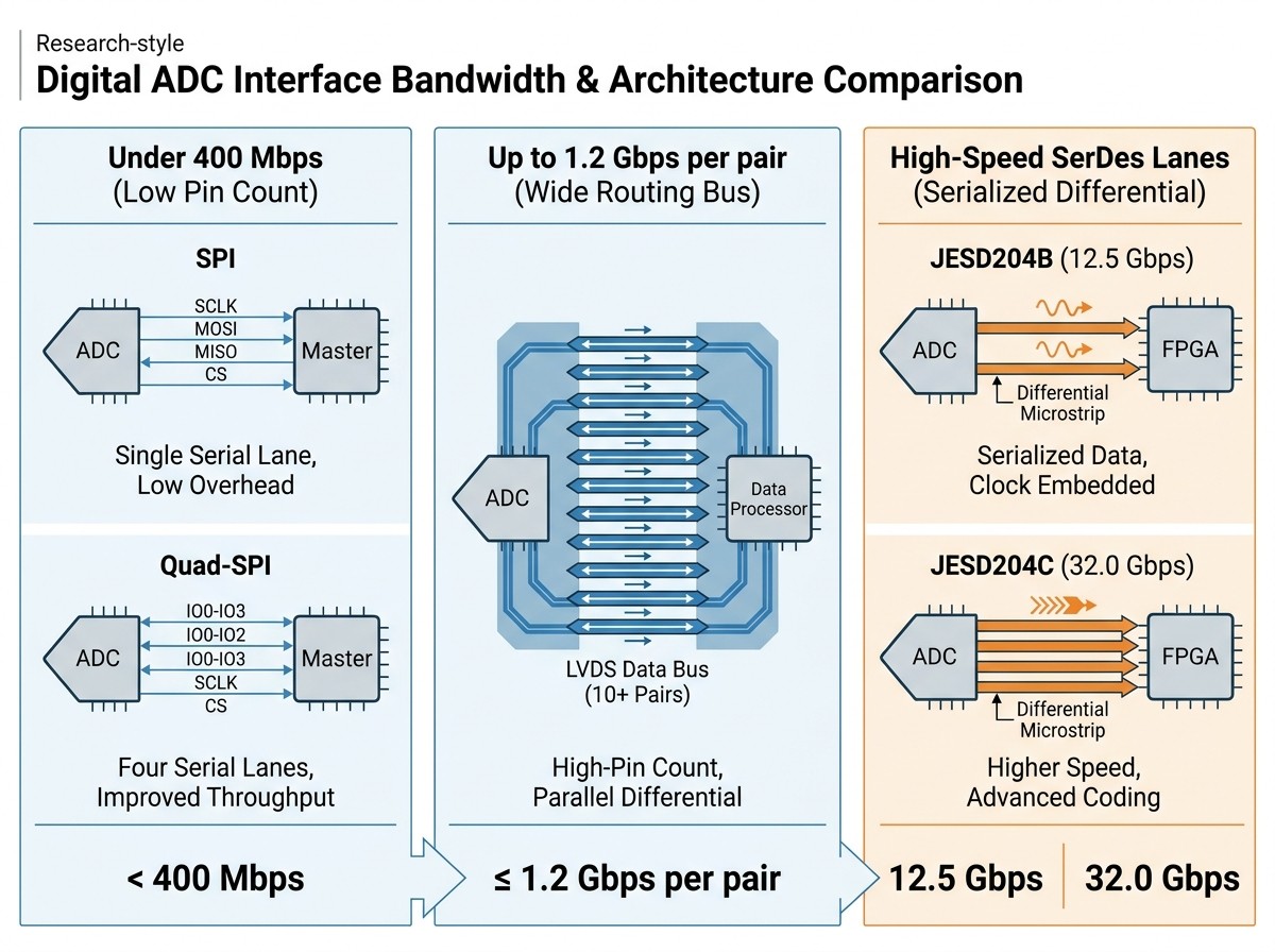
Low-to-Medium Throughput Interfaces: SPI, Dual/Quad SPI, and I2C
Standard Serial Peripheral Interface (SPI) uses single-ended signaling consisting of SCLK, MOSI, MISO, and CS.
Bandwidth Limitations: SPI serial clock speeds typically top out at 50 to 100 MHz. For a 16-bit converter running at 1 MSPS, standard SPI requires a clock frequency exceeding 16 MHz plus protocol framing overhead. Practical single-line SPI is limited to sample rates below 5 MSPS.
Multi-Lane Scaling: Dual-SPI and Quad-SPI interfaces add data output lanes to quadruple throughput without transitioning to complex differential buses, making them suitable for multi-channel industrial SAR converters.
High-Speed Parallel and LVDS Interfaces
Parallel CMOS interfaces transition an entire data bus simultaneously on a single clock edge. However, high-frequency single-ended switching induces power supply bounce and capacitive crosstalk.
Parallel Low-Voltage Differential Signaling (LVDS) overcomes CMOS single-ended limitations by driving complementary 350 mV differential swings over controlled 100 Ω differential trace pairs:
Bandwidth: Supports lane rates up to 1.0 to 1.2 Gbps per pair.
Routing Penalty: A dual-channel, 12-bit ADC operating at 1.6 GSPS requires 24 to 48 differential LVDS trace pairs (48 to 96 physical traces) plus source-synchronous clocks. This trace density quickly exhausts FPGA I/O banks and complicates PCB length-matching.
High-Speed SerDes Protocols: JESD204B vs. JESD204C
For multi-channel, multi-GSPS direct RF sampling ADCs, serialized point-to-point data transmission replaces parallel buses.
JESD204B Standard:
Data Rate: Lane rates up to 12.5 Gbps.
Encoding: 8B/10B encoding, which imposes a 20% bandwidth overhead.
Deterministic Latency: Achieved through Subclass 1 (utilizing an external periodic or pulsed SYSREF signal) and Subclass 2 (utilizing the bidirectional SYNC line).
JESD204C Standard:
Data Rate: Expands lane rates up to 32.0 Gbps per SerDes lane[6].
Encoding Efficiency: Introduces 64B/66B and 64B/80B link layers, reducing transmission overhead down to 3.125%.
Forward Error Correction (FEC): Integrated error correction maintains link reliability at ultra-high lane rates, enabling high-density multi-antenna arrays and radar direct-sampling architectures.
Digital Interface Selection Matrix
| Interface Standard | Max Data Rate (Per Lane/Bus) | Relative Pin Count | PCB Routing Complexity | Protocol Overhead | FPGA / Host IP Complexity |
|---|---|---|---|---|---|
| Standard SPI | ~ 50–100 Mbps | Low (4 wires) | Low (Single-ended routing) | Low (Frame sync bits) | None (Standard hard IP) |
| Quad SPI (QSPI) | ~ 200–400 Mbps | Moderate (6–7 wires) | Low to Moderate | Low | Very Low |
| Parallel LVDS | 1.0–1.2 Gbps / pair | High (24–96+ pins) | High (Strict length matching) | Zero | Low to Moderate (ISERDES) |
| JESD204B | 12.5 Gbps / lane | Very Low (1–8 SerDes pairs) | Moderate (High-speed diff) | 20% (8B/10B) | High (Licensed SerDes IP Core) |
| JESD204C | 32.0 Gbps / lane | Minimal (1–4 SerDes pairs) | High (Requires RF PCB stackup) | 3.125% (64B/66B) | High (SerDes IP Core + FEC) |
Mixed-Signal PCB Layout and Hardware Implementation Rules
High-resolution conversion requires strict isolation between low-level analog signals and fast digital return paths.
Grounding Architecture: Solid Ground Planes vs. Partitioning
Avoid Split Ground Planes: Splitting ground planes into isolated AGND and DGND sections frequently causes ground loop inductance. High-frequency digital currents crossing plane splits radiate EMI and induce common-mode noise.
Implement Geometric Partitioning: Maintain a single, continuous, solid ground plane. Partition the physical board layout into distinct analog and digital domains. Place the ADC directly on the boundary, routing all analog traces exclusively over the analog ground area and all digital traces over the digital ground area.
Power Supply Distribution and Decoupling Network Design
Supply Rail Isolation: Power analog rails (AVDD), digital core (DVDD), and I/O drivers (IOVDD) from dedicated linear low-dropout (LDO) regulators. When driving from switch-mode power supplies (SMPS), insert ferrite beads and LC pi-filters to attenuate switching ripple.
Decoupling Placement: Place 0.1 μF and 1.0 μF low-ESR ceramic capacitors (X7R dielectric) directly adjacent to ADC power pins on the primary layer. Minimize trace lengths and avoid inserting routing vias between the capacitor pads and the IC pins to minimize parasitic loop inductance (Ltrace).
Input Routing and Clock Distribution Hygiene
Differential Trace Symmetry: Route differential analog input traces (IN+ / IN-) with balanced lengths, matching widths, and constant inter-pair spacing to preserve common-mode rejection ratio (CMRR).
Clock Isolation: Route the ADC sampling clock trace as an RF transmission line. Shield clock paths with ground stitching vias and maintain spatial separation from digital switching buses to eliminate clock phase modulation and jitter injection.
Engineering Verification Checklist and Design Summary
Evaluating converter trade-offs requires an intent-first analytical framework—treating parameter selection not merely as data-type matching, but mapping architectural intent directly against error budgets. In visual stress tests and signal-integrity evaluations, tracking dynamic deviation against an ideal baseline reveals harmonic spurs and settling ringing far more effectively than single-point DC measurements.
Chart Selection Guide – Visual Vocabulary
System Design Verification Checklist:
[ ] 1. Architecture Latency: Verified that conversion latency does not compromise closed-loop feedback or multiplexer channel switching.
[ ] 2. Dynamic ENOB: Calculated target ENOB at max operating input frequency (fin), not just at DC.
[ ] 3. Kickback Settling: Verified that front-end RC time constants satisfy tacq ≥ (N + 1) · ln(2) · τ in SPICE simulation.
[ ] 4. Driver Stability: Ensured front-end op-amp has adequate phase margin when driving the external filter capacitor (Cfilt).
[ ] 5. Jitter Floor: Confirmed clock phase noise meets SNRjitter = -20 log10(2π fin tj) for target high-frequency ENOB.
[ ] 6. Reference Drift: Budgeted reference tempco (ppm/°C) to ensure gain error across temperature remains within total system LSB limits.
[ ] 7. Interface Bandwidth: Matched SPI/LVDS/JESD204C throughput to FPGA/host processing capabilities and routing constraints.
[ ] 8. Solid Grounding: Placed converter on a unified, continuous ground plane with clear geometric component partitioning.
Community Consensus and Practical Field Observations
On engineering design forums and in hardware lab reviews, several common implementation challenges are consistently highlighted:
The "Missing ENOB" Phenomenon: Users on community forums frequently report losing 3 to 4 bits of nominal resolution on their first hardware spin. Real-world troubleshooting almost always identifies front-end settling errors (undersized acquisition time or wrong RfiltCfilt ratio) or power supply ripple coupling into the unbuffered voltage reference pin.
Multiplexer Settling Oversights: A common consensus among mixed-signal engineers is that multiplexing high-impedance sensor channels into a single high-speed SAR ADC requires active buffer isolation per channel. Trying to settle full-scale differential steps between channels across an unbuffered multiplexer degrades accuracy.
Frequently Asked Questions
Why does a 16-bit ADC only deliver 12 effective bits during bench measurements?
This discrepancy occurs because nominal resolution reflects only quantization step count, whereas Effective Number of Bits (ENOB) accounts for all real-world noise and distortion sources (ENOB = (SINAD - 1.76 dB) / 6.02).
Common causes of degraded ENOB include:
Incomplete front-end RC settling during the acquisition window (tacq).
Clock aperture jitter injecting phase noise at high input frequencies.
Unfiltered noise or thermal drift on the external voltage reference pin.
Switching ripple from switch-mode power supplies coupling into the AVDD rail.
When is an oversampled SAR ADC preferred over a Delta-Sigma ADC?
An oversampled SAR ADC is preferred when an application requires both high dynamic range and rapid response to transient events. SAR converters provide zero conversion latency, allowing them to switch between multiplexed channels or respond immediately in closed-loop control loops (e.g., motor drives).
Delta-Sigma ADCs deliver higher ultimate resolution (up to 24 to 32 bits), but their internal digital decimation filters introduce multi-cycle group delays that slow response times during channel switching or fast step changes.
How does digital filter group delay in Delta-Sigma ADCs affect real-time closed-loop control?
The digital decimation filter (typically sinc or FIR filters) inside a Delta-Sigma converter averages multiple modulator cycles to eliminate out-of-band quantization noise.
This filtering creates a deterministic phase lag (group delay) between the analog input event and the digital word output. In high-bandwidth feedback systems, this phase lag erodes the phase margin of the feedback loop, potentially inducing loop oscillation or instability.
What is the practical throughput limit before SPI must be replaced with parallel LVDS or SerDes?
Standard SPI operates reliably with serial clock speeds up to 50 to 100 MHz. For a single-channel 16-bit converter running at 1 MSPS, the data interface requires at least 16 Mbps of sustained throughput.
When sample rates exceed 5 MSPS—or when multiplexing multiple high-resolution channels—standard single-line SPI bus speeds become insufficient. Engineers must then transition to Dual/Quad SPI, parallel LVDS, or JESD204B/C SerDes protocols to prevent interface bottlenecks.
How do I determine whether my design requires an external precision voltage reference?
Calculate the error budget over the product's operating temperature range. Internal ADC references typically exhibit drift rates of 20 to 50 ppm/°C. In a 16-bit system (1 LSB = 15.26 ppm), a 30°C temperature rise shifts an internal 25 ppm/°C reference by 750 ppm, consuming roughly 49 LSBs of gain error.
If the calculated reference drift exceeds your system's total allowable DC error budget, an external low-drift reference (< 1 to 5 ppm/°C) is mandatory.
References
MT-001 Tutorial: Taking the Mystery out of the Infamous Formula, "SNR = 6.02N + 1.76dB," and Why You Should Care — Analog Devices
MT-003 Tutorial: Understand SINAD, ENOB, SNR, THD, THD + N, and SFDR so You Don't Get Lost in the Noise Floor — Analog Devices
MT-007 Tutorial: Aperture Time, Aperture Jitter, Aperture Delay Time - Removing the Confusion — Analog Devices
AN-742 Application Note: Frequency Domain Response of Switched Capacitor ADCs — Analog Devices
Switched-Capacitor ADC Analog Input Calculations (Application Report SLAA036) — Texas Instruments
What to Know About the Differences Between JESD204B and JESD204C (White Paper SLYY171) — Texas Instruments
Jitter vs SNR for ADCs (TI Precision Labs TIPL 4704) — Texas Instruments
IN5220: Switched-Capacitor Circuits — University of Oslo
 UTMEL
UTMEL
We are the professional distributor of electronic components, providing a large variety of products to save you a lot of time, effort, and cost with our efficient self-customized service. careful order preparation fast delivery service
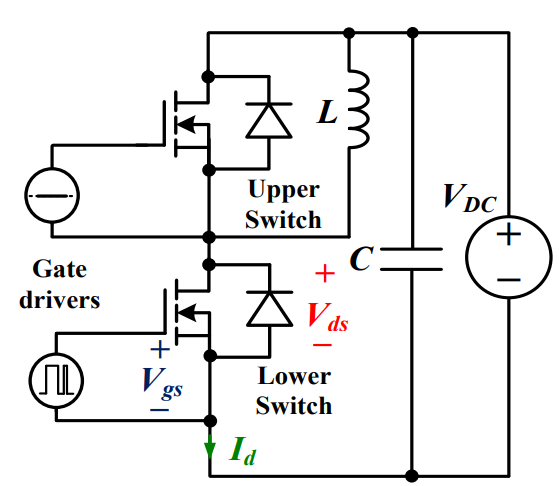 Discovering New and Advanced Methodology for Determining the Dynamic Characterization of Wide Bandgap DevicesSaumitra Jagdale15 March 20242862
For a long era, silicon has stood out as the primary material for fabricating electronic devices due to its affordability, moderate efficiency, and performance capabilities. Despite its widespread use, silicon faces several limitations that render it unsuitable for applications involving high power and elevated temperatures. As technological advancements continue and the industry demands enhanced efficiency from devices, these limitations become increasingly vivid. In the quest for electronic devices that are more potent, efficient, and compact, wide bandgap materials are emerging as a dominant player. Their superiority over silicon in crucial aspects such as efficiency, higher junction temperatures, power density, thinner drift regions, and faster switching speeds positions them as the preferred materials for the future of power electronics.
Read More Applications of FPGAs in Artificial Intelligence: A Comprehensive GuideUTMEL29 August 20255535
This comprehensive guide explores FPGAs as powerful AI accelerators that offer distinct advantages over traditional GPUs and CPUs. FPGAs provide reconfigurable hardware that can be customized for specific AI workloads, delivering superior energy efficiency, ultra-low latency, and deterministic performance—particularly valuable for edge AI applications. While GPUs excel at parallel processing for training, FPGAs shine in inference tasks through their adaptability and power optimization. The document covers practical implementation challenges, including development complexity and resource constraints, while highlighting solutions like High-Level Synthesis tools and vendor-specific AI development suites from Intel and AMD/Xilinx. Real-world applications span telecommunications, healthcare, autonomous vehicles, and financial services, demonstrating FPGAs' versatility in mission-critical systems requiring real-time processing and minimal power consumption.
Read More The 2026 Engineer’s Guide: Choosing the Right MCU for Your Next IoT & New Energy ProjectUTMEL30 April 20261764
A comprehensive comparison of 2026's leading MCUs from ST, NXP, and Microchip across power efficiency, processing performance, connectivity, and ecosystems to help engineers select the optimal chip for next-gen IoT and new energy projects.
Read More AI Server Components: Engineering Next-Gen Data Center Hardware for 100kW RacksUTMEL15 May 2026967
The transition from traditional enterprise IT to AI-driven workloads has rendered legacy data center hardware obsolete, forcing infrastructure planners to re-engineer server components for extreme thermal environments.
Read More The Practical Engineer’s Guide to the NE555N Timer: Pinout, Setup, and TroubleshootingUTMEL29 May 2026750
This comprehensive guide explores the NE555N timer, detailing its 8-pin layout, internal architecture, and key datasheet specifications. It compares the bipolar IC to CMOS variants and details setup configurations for astable, monostable, and bistable modes. Additionally, the guide offers practical troubleshooting advice to prevent common breadboard failures, such as floating reset pins and electrical noise issues.
Read More
Subscribe to Utmel !
![ACPL-337J-500E]() ACPL-337J-500E
ACPL-337J-500EBroadcom Limited
![ADUM3223BRZ-RL7]() ADUM3223BRZ-RL7
ADUM3223BRZ-RL7Analog Devices Inc.
![AD5522JSVDZ]() AD5522JSVDZ
AD5522JSVDZAnalog Devices Inc.
![ACPL-W343-500E]() ACPL-W343-500E
ACPL-W343-500EBroadcom Limited
![HCS515-I/SL]() HCS515-I/SL
HCS515-I/SLMicrochip Technology
![FOD3150S]() FOD3150S
FOD3150SON Semiconductor
![1EDI20I12AFXUMA1]() 1EDI20I12AFXUMA1
1EDI20I12AFXUMA1Infineon Technologies
![AT88SC0104CA-SH-T]() AT88SC0104CA-SH-T
AT88SC0104CA-SH-TMicrochip Technology
![SI8233BD-D-IS]() SI8233BD-D-IS
SI8233BD-D-ISSilicon Labs
![FOD3180SD]() FOD3180SD
FOD3180SDON Semiconductor


