

 Product
 Brand
 Articles
 Tools

Automotive MCU Allocation Spillover 2026: Lead Times, Industrial Buyers, and Second-Source Qualification
Quick Answer: Evaluating automotive mcu lead time 2026 requires looking past blended market averages to track selective, mature-node allocation across 28nm, 40nm, and 90nm+ embedded non-volatile memory (eNVM) foundry lines. While standard catalog microcontrollers carry directional planning lead times of roughly 14 to 26 weeks, mainstream automotive control families average 26 to 40 weeks, and constrained functional-safety or electrification MPNs stretch from 30 to 52+ weeks. Because nominal distributor portal quotes frequently lag actual factory delivery for uncontracted buyers, procurement and engineering teams locking late-October RFQs for 2027 production must verify live commitments per exact MPN suffix and triage their bills of materials (BOMs) using a structured three-scenario second-source framework.
As automotive Tier-1 suppliers and industrial OEMs finalize annual framework agreements in late October 2026, supply chain risk has shifted from broad-based wafer shortages to acute, family-level bottlenecks. Ongoing market intelligence from TrendForce's automotive MCU analysis and late-2026 industrial hardware advisories from Meerstetter Engineering highlight how tightening capacity on shared mature process nodes spills over into industrial automation, energy, and medical equipment lines. For a broader view of cross-category supply dynamics heading into next year, review our 2026 Q4 Electronic Components Market Analysis Report: Supply, Pricing, and Procurement Outlook.
Before diving into vendor-specific allocation patterns or rewriting embedded firmware, procurement leads and hardware engineers must align on what "qualifying a second source" actually means for a delayed part number.
The 3-Scenario Second-Source Decision Framework
Not every allocation notice justifies a board respin. Use this three-tier triage model to match your mitigation path to your production timeline and engineering bandwidth:
Scenario A: Same Exact MPN, Alternate Authorized Channel or Franchise Buffer
Best For: Bridging immediate Q4 2026 and Q1 2027 production gaps without altering hardware layouts or software baselines.
Strength: Zero PCB layout or firmware modifications; preserves existing Production Part Approval Process (PPAP) compliance when sourced with complete manufacturer lot traceability.
Drawback and Hidden Risk: Exposure to spot-market price premiums; requires rigorous incoming inspection for date codes, Moisture Sensitivity Level (MSL) dry-pack integrity, and RoHS/REACH documentation.
Who Should Not Choose This: Programs facing a multi-quarter factory wafer allocation freeze where global authorized channel inventory is exhausted across all packaging variants.
Scenario B: Same Base MPN, Alternate Wafer Fab, Assembly Site, or Die Revision (PCN Approval)
Best For: Unlocking parallel factory allocation—such as dual-frontend 40nm/90nm wafer fabs or secondary QFP/BGA back-end assembly houses—offered by the original semiconductor manufacturer.
Strength: Retains pin-to-pin footprint compatibility, core peripheral register maps, and existing AUTOSAR or bare-metal software architectures.
Drawback and Hidden Risk: Requires auditing vendor Product Change Notifications (PCNs), reviewing AEC-Q100 lot equivalence reports, and executing a customer delta-PPAP that typically consumes 1.5 to 3 months.
Who Should Not Choose This: Teams whose automotive OEM customer enforces a frozen hardware baseline without an expedited delta-PPAP review pathway.
Scenario C: Cross-Family or Cross-Vendor MCU Substitution (Hardware and Firmware Redesign)
Best For: Next-generation 2027–2028 platform builds or severe, multi-quarter single-source allocation lockouts on legacy nodes.
Strength: Permanently eliminates single-vendor allocation and pricing leverage by establishing a dual Approved Vendor List (dual-AVL).
Drawback and Hidden Risk: High engineering friction requiring 4 to 9+ months to resolve pinout deviations, flash memory wait-state penalties, proprietary peripheral IP differences, AUTOSAR Microcontroller Abstraction Layer (MCAL) licensing, electromagnetic compatibility (EMC) chamber re-testing, and full PPAP sign-off.
Who Should Not Choose This: Teams attempting to rescue a line-down crisis occurring within the next 60 to 90 days.
Table 1: Indicative 2026–2027 Automotive & Industrial MCU Lead-Time Planning Ranges
Note: All lead-time figures below represent directional industry and distributor planning baselines synthesized from market trackers and OEM supply advisories. Actual delivery varies by customer tier, package suffix, and factory backlog; buyers must confirm live quotes for every specific MPN.
| MCU Category & Foundry Node Profile | Indicative Planning Range (Weeks) | Primary Bottleneck Driver | Recommended Procurement & Engineering Action |
|---|---|---|---|
| Standard 8-bit / 32-bit Catalog & Legacy Industrial MCUs | ~14–26 weeks (Directional) | Routine back-end wire-bond packaging queues and seasonal order batching | Maintain rolling 6-to-12-month forecasts; pre-approve tape-and-reel vs. tray and temperature suffix alternates on the BOM. |
| Mainstream Automotive Body, Cabin & Industrial Control MCUs (90nm–180nm eNVM) | ~26–40 weeks (Directional) | Shared mature-node wafer capacity across automotive body ECUs and industrial automation | Lock annual framework schedules covering at least 75% of forecasted demand; evaluate Scenario B dual-fab/assembly PCNs. |
| Constrained / Allocated Automotive Safety, Zone & Electrification MCUs (28nm / 40nm eNVM) | ~30–52+ weeks (Directional) | Tight embedded flash/RRAM foundry slots, high-pin-count BGA packaging, and platform transitions | Demand written factory allocation in late-Oct RFQs; audit companion PMIC rails; initiate Scenario C dual-AVL qualification for 2027 builds. |
Why Market Averages Mislead: MPN- and Family-Level Allocation Patterns (ST, NXP, Renesas, Infineon)
Automotive microcontroller supply concentrates heavily around five foundational semiconductor vendors—NXP Semiconductors, Infineon Technologies, Renesas Electronics, Texas Instruments, and STMicroelectronics[8]—which together anchor the global automotive IC landscape, as documented by Electronics Weekly. Unlike consumer smartphones or data center accelerators that rely on leading-edge 3nm or 5nm logic, automotive and industrial control units depend on specialized 28nm, 40nm, and 90nm+ embedded non-volatile memory (eNVM) processes capable of withstanding extreme thermal cycling while storing deterministic real-time code on-chip.
A single modern vehicle distributes compute across more than 40 distinct electronic control subsystems—ranging from legacy body and chassis nodes (Adaptive Front Lighting, Electronic Stability Control, Tire Pressure Monitoring, and Blindspot Detection) to high-compute electrification and cabin domains (Battery Management Systems, Regenerative Braking, Active Cabin Noise Suppression, Night Vision, and Head-Up Displays). Because each domain requires specific safety, transceiver, and thermal footprints, an allocation crunch on a single QFP or BGA microcontroller halts assembly for the entire module. For background on how these domains partition across vehicle architectures, see our Comprehensive Guide to Car Chips FAQs.
What is Automotive Microcontroller's || How they are different from Arduino-STM32-ESP MCU's
Market intelligence bulletins from TrendForce's coverage of European and Asian chipmakers show that supply pressure in late 2026 is driven by structural node transitions and eNVM wafer allocation across four major MCU architectures:
STMicroelectronics: Exhibits high industrial and automotive crossover across general-purpose STM32 (H7, H5, G4, F4) and legacy STM8 lines, alongside dedicated automotive SPC5 and Stellar families. In electrification architectures, ST's Stellar E series—specifically the
SR5E1E7(alongsideSR5E1E3andSR5E1E5) in high-pin-count QFP packages—is manufactured on a 40nm embedded flash (eFlash) process featuring dual 32-bit Arm Cortex-M7 cores operating in split or lockstep mode, 2 MB of Flash, a Hardware Security Module (HSM), and ASIL-D compliance for EV on-board chargers (OBC) and DC/DC converters. Heavy demand on shared 90nm and 40nm eFlash lines directly links automotive OBC ramps to industrial STM32 lead-time stretch.NXP Semiconductors: Faces structural transition tension between established S32K1 body/zone controllers (such as the widely deployed
S32K144in LQFP and MAPBGA packages) and high-demand 28nm S32K3 safety and electrification families. As OEMs migrate zone architectures to multi-core S32K3 BGA/LQFP derivatives, extended order backlogs require early 2027 schedule locks to secure wafer and back-end test slots.Infineon Technologies: Anchors a substantial share of global ADAS, powertrain, and zone-controller sockets, supported by the scale documented in Infineon's corporate investor reporting[2]. Infineon's mainstream AURIX TC3xx family relies on 40nm eFlash technology (up to six TriCore cores, ASIL-D compliant) utilizing a dual-frontend fab concept for supply continuity. Meanwhile, the next-generation AURIX TC4xx platform transitions to 28nm silicon technology (in partnership with TSMC) and replaces traditional eFlash with resistive RAM (RRAM-NVM, up to 24 MB on-chip NVM with TriCore 1.8 running up to 500 MHz). Simultaneously managing peak mature demand on 40nm
TC3xxand Traveo II body families while ramping 28nmTC4xxcreates localized package and suffix tightness alongside industrial XMC microcontrollers.Renesas Electronics: Balances tight capacity across core 32-bit RH850 powertrain/chassis MCUs and 16-bit RL78 actuator/sensor controllers. In March 2026, Renesas expanded its lineup with the 28nm RH850/U2C series (up to four cores at 320 MHz, 8 MB flash, ASIL-D, and CAN-XL support) as a next-generation migration target from legacy 40nm
RH850/P1xandF1xseries. During this multi-year overlap, legacy 40nm QFP and BGA automotive sockets remain sensitive to wafer allocation shifts.
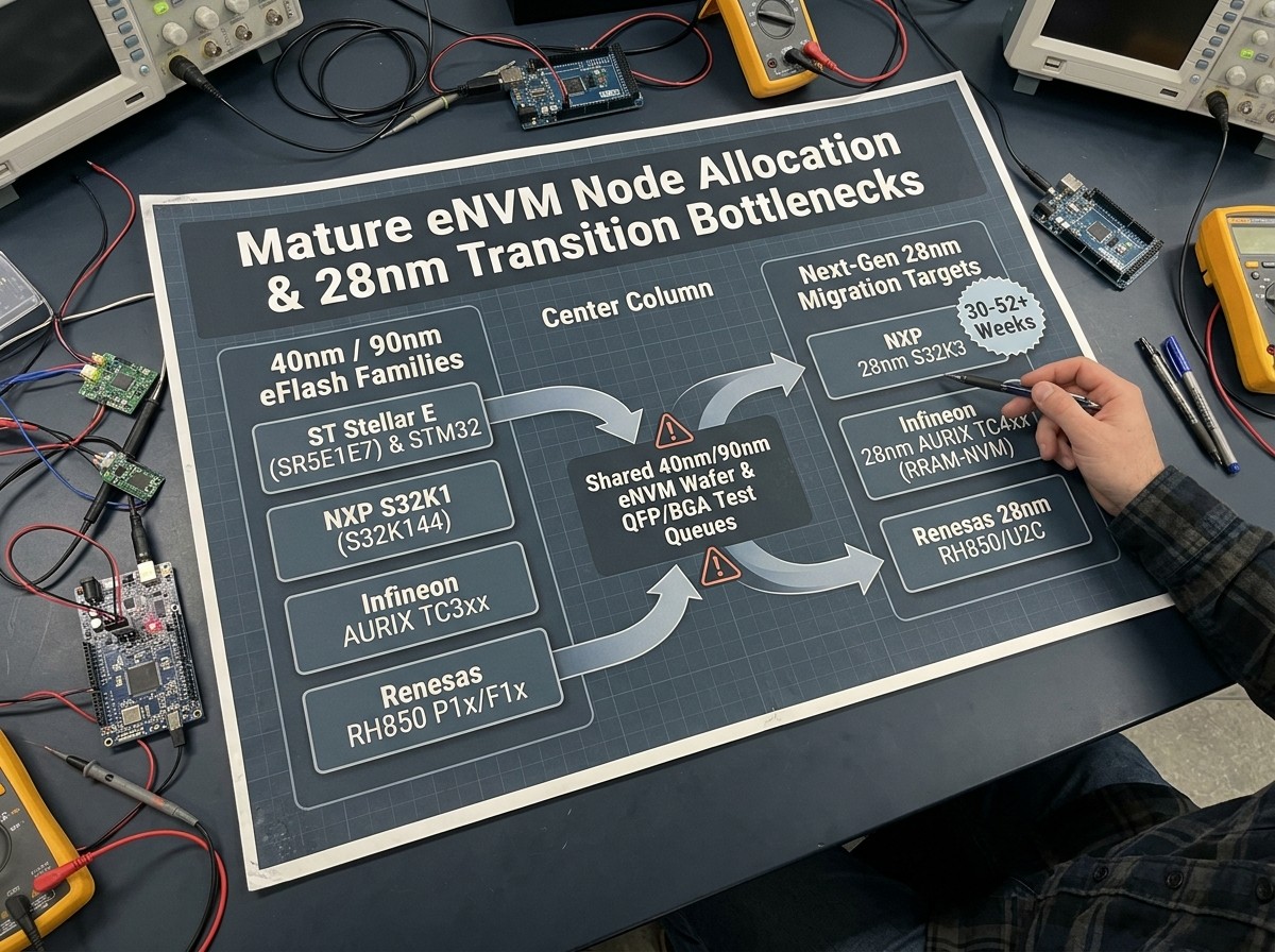
Table 2: Family-Level Allocation & Transition Patterns Across Major MCU Vendors
| Vendor | Core Automotive Families | Industrial Spillover / Shared Families | Primary Structural Supply Driver | What Buyers Must Verify in 2027 RFQs |
|---|---|---|---|---|
| STMicroelectronics | Stellar E (SR5E1E7), SPC5, STM32A | STM32 (F4, G4, H5, H7), STM8 | Shared 40nm and 90nm eFlash wafer demand across EV power conversion and industrial control | Confirm exact QFP/BGA package allocation and lock rolling STM32 framework schedules early. |
| NXP Semiconductors | S32K1 (S32K144), S32K3, S32G | LPC series, i.MX RT crossover MCUs | Platform migration backlog from mature S32K1 nodes to 28nm S32K3 safety/zone controllers | Verify whether quoted lead times apply to legacy LQFP suffixes or constrained 28nm MAPBGA lots. |
| Infineon Technologies | AURIX (TC3xx, TC4xx), Traveo II | XMC1000 / XMC4000, PSoC Industrial | Transition from 40nm eFlash (TC3xx) to 28nm RRAM-NVM (TC4xx); high-pin-count BGA test time | Check dual-frontend fab PCN approval status (Scenario B) and audit companion OPTIREG PMIC availability. |
| Renesas Electronics | RH850 (P1x, F1x, 28nm U2C), RL78/F | RL78 general-purpose, RA & RX 32-bit | Overlap between mature 40nm RH850 chassis/powertrain demand and 28nm RH850/U2C platform ramps | Confirm live delivery commitments per exact QFP/BGA suffix rather than relying on family-wide portal averages. |
Why Search Summaries, Market Reports, and Portals Disagree on 2026 Lead Times
Procurement teams often encounter contradictory signals when researching automotive mcu lead time 2026: one high-level market summary may claim semiconductor lead times have normalized below 20 weeks, while an authorized distributor quotes 42+ weeks for an automotive safety MPN. Three structural factors explain this discrepancy:
The Bimodal Distribution Trap: Blending high-volume, general-purpose 8-bit and 32-bit catalog MCUs (sitting at 14–18 weeks) with allocated 28nm and 40nm eNVM automotive safety MCUs (stretching to 35–52+ weeks) yields a mathematically deceptive ~18-week "average." A single allocated BGA microcontroller on a 45-week lead time halts PCB assembly regardless of how fast the other 200 passive and logic components arrive.
Suffix-Level Blindness: Macro industry trackers monitor vendor revenue rather than part-number suffixes. Within the exact same MCU family, a standard LQFP-100 Grade 1 (
-40°Cto+125°C) suffix may have buffer stock, while the high-density BGA Grade 0 (-40°Cto+150°C) suffix is fully allocated to Tier-1 powertrain contracts through mid-2027.Outdated Commodity Assumptions: Generic supply summaries treat 32-bit microcontrollers as interchangeable commodities, overlooking the reality that proprietary peripheral IP, functional safety manuals, and hardware security modules lock buyers into specific silicon for the life of a vehicle program.
Franchise LTA Priority vs. Spot Exposure: Why Quoted Lead Times Slip
A Nominal Quoted Lead Time is the baseline manufacturing cycle time displayed on a distributor portal assuming unconstrained material flow, whereas a Committed Factory Delivery Date represents a specific wafer-start and back-end assembly slot contractually bound to your purchase order. When mature foundry capacity tightens, unforecasted buyers discover that placing a standard purchase order against a 20-week portal quote frequently results in delivery push-outs of 6 to 16+ weeks once the factory processes the backlog.
The 3-Tier Semiconductor Allocation Waterfall
Integrated Device Manufacturers (IDMs) and wafer foundries partition constrained 28nm, 40nm, and 90nm eNVM wafer starts and wire-bond/BGA test capacity through a strict three-tier priority waterfall:
Tier 1: Contracted Automotive OEM and Tier-1 LTA / NCNR Backlog
Allocation Mechanics: Receives first claim on wafer starts, die banks, and assembly slots locked 6 to 12 months in advance under Non-Cancelable, Non-Returnable (NCNR) agreements or annual Long-Term Agreements (LTAs).
Tier 2: Franchise Distributor Scheduled Program Buffers
Allocation Mechanics: Receives secondary factory allocation reserved for recurring contract customers who maintain rolling 12-month EDI forecasts and scheduled monthly release windows.
Tier 3: Unforecasted Spot and Standard Portal Purchase Orders
Allocation Mechanics: Competes for residual wafer and packaging capacity. Whenever a Tier-1 automotive account exercises contractual upside flex or a back-end assembly line experiences a test bottleneck, Tier 3 orders are the first to be de-committed and rescheduled.
Real-world industry advisories underscore how quickly this waterfall impacts industrial and mid-sized buyers. In a customer supply notice issued on August 19, 2026, industrial OEM Meerstetter Engineering warned of tightening component supply, price volatility, and extended replenishment lead times across selected STM32 microcontrollers and high-volume industrial ICs—explicitly recommending that customers lock 75% of their expected demand through February 2027 via scheduled framework agreements.
Comparing 2027 Procurement Commitment Models
Direct or Franchise Annual LTA & NCNR Lock
Best For: High-volume, stable production BOMs with predictable quarterly run rates.
Strength: Secures Tier-1 factory wafer priority and shields against mid-year spot price spikes.
Drawback: Zero downward volume flexibility if end-market demand softens.
Who Should Avoid: Early-stage designs or NPI builds where MPN suffixes or PCB layouts may still change.
Franchise Rolling Buffer & Scheduled Pipelining
Best For: Mid-volume industrial OEMs and Tier-2 automotive module builders.
Strength: Balances working capital outlays with dedicated distributor safety stock.
Drawback: Buffer depletion risk if upstream factory lead times stretch faster than the replenishment window.
Who Should Avoid: Buyers unwilling to commit to rolling 6-to-12-month forecast visibility.
Agile B2B Spot & Alternative Distribution Sourcing
Best For: Bridging unforecasted demand surges, LTA de-commits, and engineering prototype runs (
Scenario A).Strength: Immediate access to global market liquidity and cross-grade authorized stock.
Drawback: Unit pricing reflects live supply-demand tightness; requires strict vendor vetting.
Who Should Avoid: Procurement teams lacking incoming quality control (IQC), lot traceability verification, and anti-counterfeit screening protocols.
Auto AEC-Q100 vs. Industrial Spillover: Shared Fabs, Temperature Grades, and Substitution Boundaries
Industrial equipment manufacturers—building programmable logic controllers (PLCs), servo motor drives, solar inverters, and medical diagnostic gear—experience acute component shortages during automotive allocation cycles because both sectors share the exact same 40nm, 90nm, 130nm, and 180nm wafer fabrication lines and back-end LQFP/QFN wire-bond assembly facilities. When automotive Tier-1 suppliers lock wafer capacity, industrial MCU lead times stretch in tandem, forcing engineering and procurement teams to evaluate cross-grade substitution under strict reliability boundaries.
As detailed in Design & Reuse's technical overview of automotive qualification and Infineon's official AEC-Q100 specification guide[1], AEC-Q100 is the mandatory failure-mechanism-based stress-test standard governing packaged integrated circuits (including microcontrollers, sensors, and memory chips)[7] in automotive applications. Updated to AEC-Q100 Rev J1 on March 24, 2026, the standard enforces rigorous multi-lot verification that far exceeds standard commercial or industrial JEDEC qualification flows:
Multi-Lot Zero-Defect Sampling: Core stress tests require sampling 77 parts per lot across 3 distinct wafer fabrication lots (231 units total) with zero permissible failures (0 defects).
Accelerated Lifetime and Environmental Stress: Includes 1,000-hour High-Temperature Operating Life (HTOL) testing, 500 to 1,500 temperature cycles (depending on grade), Human Body Model (HBM) and Charged Device Model (CDM) electrostatic discharge characterization, and latch-up testing.
System-Level Zero-Defect Controls: As emphasized by EE Times[5] and EDN[6], true automotive quality extends beyond baseline stress tests to encompass Part Average Testing (PAT) for statistical outlier rejection, IATF 16949 certified manufacturing flows, and formal vendor qualification workflows like those documented for Lattice Semiconductor's AEC-Q100 devices[3].
Ambient Temperature Grade Boundaries: Selecting an alternate suffix requires matching the exact ambient thermal envelope (
T_A) to the ECU mounting location, a boundary frequently analyzed in engineering forums such as Texas Instruments' E2E Grade 0 vs. Grade 1 technical discussion. For a deep dive into how these ratings affect part selection, consult our guide on Decoding AEC-Q100: A Sourcing Guide to Automotive-Grade Semiconductor Qualification and Temperature Ratings.
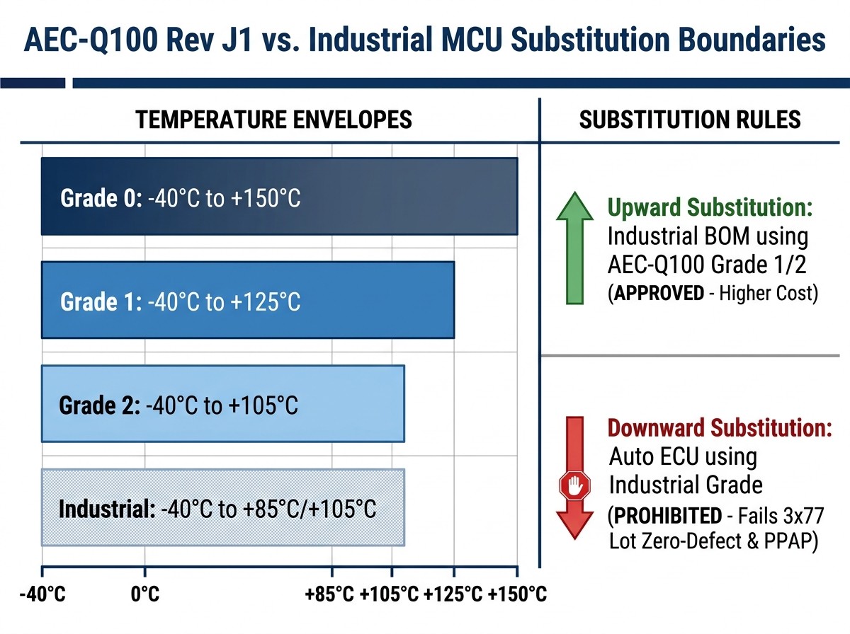
Table 3: Automotive (AEC-Q100) vs. Industrial-Grade MCU Qualification & Spillover Matrix
| Qualification Parameter | Automotive Grade (AEC-Q100 Rev J1) | Standard Industrial Grade | 2026–2027 Allocation Spillover Impact |
|---|---|---|---|
| Governing Reliability Standard | Auditable AEC-Q100 stress flow: 3 lots x 77 units with 0 defects across 1,000-hr HTOL & temp cycling | Vendor-specific JEDEC reliability qualification (typically single-lot or internal stress metrics) | Automotive wafers require dedicated fab lot tracking and extended probe/burn-in test times. |
| Ambient Temperature Grades | Grade 0: -40°C to +150°C (Engine/Transmission)Grade 1: -40°C to +125°C (Powertrain/Chassis)Grade 2: -40°C to +105°C (Body/Cabin)Grade 3: -40°C to +85°C | Typically -40°C to +85°C or -40°C to +105°C | Industrial buyers can use Grade 1/2 parts seamlessly; auto buyers must never downgrade a Grade 0 under-hood socket to Grade 1/Industrial. |
| Quality Management & Traceability | Mandatory IATF 16949 fab/assembly certification, full PPAP documentation, and PAT outlier screening | Standard ISO 9001 quality management and standard Certificate of Conformance (CoC) | Lack of PPAP and 3-lot traceability legally blocks industrial suffixes from series automotive production. |
| Functional Safety & Hardware Security | Integrated ISO 26262 ASIL-B/D hardware IPs (lockstep cores, ECC, LBIST) and SHE/HSM crypto engines | Rarely includes certified safety manuals or full automotive HSM firmware stacks | Downward substitution breaks safety diagnostics and secure boot toolchains. |
| BOM Cost Structure | Carries an automotive qualification and testing premium | Baseline industrial pricing | Upward substitution increases industrial BOM cost per unit but prevents costly factory line-downs. |
Substitution Boundaries: Who Should (and Should Not) Cross Grades
Path 1: Upward Substitution (Industrial Buyer Using Automotive AEC-Q100 Stock)
Application Boundary: Technically safe and electrically over-engineered for
-40°Cto+85°Cor+105°Cindustrial environments. When an industrial STM32, S32K, or RL78 suffix is on allocation, approving the-Q1or AEC-Q100 Grade 1/2 equivalent is a proven way to keep lines running.Trade-Off: You absorb an automotive unit price premium on your industrial BOM and must verify that automotive-specific defaults (such as lockstep core supervision or hardware watchdog timers) match your industrial initialization code.
Path 2: Downward Substitution (Automotive Buyer Eyeing Industrial or General-Purpose Stock)
Application Boundary and Common Mistake: Strictly prohibited for series automotive production. Attempting to mitigate an automotive MCU shortage by dropping in an uncertified industrial suffix—or a general-purpose development chip like an entry-level commercial STM32, ESP32, or Arduino-class microcontroller—violates AEC-Q100 stress mandates, breaches IATF 16949 and OEM PPAP contracts, and fails software integration. General-purpose microcontrollers do not support automotive software ecosystems (AUTOSAR MCAL, ISO 26262 hardware safety IPs, HSM/SHE cryptography, and MATLAB Model-Based Design toolboxes), which exist exclusively on true automotive architectures like NXP S32, Renesas RH850, Infineon AURIX TriCore, ST Stellar, and TI Sitara.
The Only Valid Exception: Early-stage software bench bring-up, GUI toolchain evaluation, or laboratory Hardware-in-the-Loop (HIL) test rigs while waiting for allocated AEC-Q100 engineering samples to arrive (or non-safety aftermarket accessories backed by a formal, written OEM engineering deviation waiver).
Practical Second-Source Qualification Path: Pinout, Flash/Peripheral Map, and Firmware Porting Months
When an allocated microcontroller cannot be resolved through authorized channel sourcing (Scenario A) or a dual-fab PCN approval (Scenario B), engineering teams face Scenario C: Cross-Family or Cross-Vendor MCU Substitution. Qualifying a different MCU family is a 4-to-9+ month engineering program—never a simple firmware recompile. Even when two candidate MCUs share an identical 32-bit Arm Cortex-M core and nominal LQFP or BGA pin count, low-level hardware and toolchain divergences dictate the real calendar timeline.
1. Hardware, Pinout, and Package Footprint Datasheet Verification Checklist
Before committing to a candidate second-source MCU, hardware engineers must audit five physical and electrical boundaries:
Package Body and Pitch Geometry: Verify exact body dimensions, lead pitch, and exposed thermal pad geometry across high-density QFP packages (such as Renesas
RH850or ST StellarSR5E1E7) and fine-pitch BGA footprints (such as NXPS32KMAPBGA or InfineonAURIX TriCoreBGA packages).Power, Ground, and Core Ballast Pins: Audit non-multiplexed
VDD/VSSdecoupling pairs and internal core voltage regulator ballast capacitor pins (VCAP). Swapping a power pin with a high-speed GPIO guarantees a PCB respin.Reset, Clock, and Reference Pins: Confirm exact pin alignment and electrical thresholds for hardware reset (
NRST), external crystal oscillator inputs/outputs (OSC_IN/OSC_OUT), and precision ADC voltage reference pins (VREF+/VREF-).Boot-Mode Strapping: Check hardware boot configuration pins to ensure external pull-up or pull-down resistors on the board do not accidentally force the alternate MCU into factory bootloader or debug lockout mode at power-on.
Dual-Footprint PCB Layout Strategy: During initial NPI layout for 2027 builds, engineers can route a configurable dual-footprint schematic using unpopulated 0-ohm resistor jumpers to accommodate minor pin-multiplexing shifts between two candidate MCUs—saving a 10-to-12-week PCB respin and full EMC chamber re-design if the primary MPN goes on allocation.
2. Flash Memory Geometry, Wait States, and Proprietary Peripheral IP Mapping
Matching total Flash and SRAM kilobytes on a high-level datasheet comparison is one of the most common traps in second-source qualification:
Flash Sector Geometry and Wait-State Penalties: Engineers must compare minimum flash sector and page erase sizes, which directly govern bootloader memory partitioning, Over-The-Air (OTA) update swap buffers, and Data Flash / EEPROM emulation wear-leveling algorithms. Furthermore, if the alternate MCU's embedded flash array has a slower read access time at your target clock frequency, the CPU must insert additional flash wait states—degrading instruction fetch determinism and altering critical interrupt latency in motor control or braking loops.
Vehicle Network and Peripheral IP Divergence: As outlined in DigiKey's engineering guide to selecting automotive-qualified MCUs, engineers must validate processing speed, thermal resilience, and primary vehicle communication networks (CAN / CAN-FD, LIN, and Automotive Ethernet)[4]. However, even when two MCUs feature nominal CAN-FD and LIN controllers, their underlying silicon IP blocks and message RAM structures differ completely.
The Proprietary Peripheral Trap (NXP S32K144 Case Study): Consider the hardware peripheral architecture inside NXP's S32K1xx family (such as the S32K144, running an Arm Cortex-M4F at up to 80 MHz in normal RUN mode or 112 MHz in HS-RUN mode, ASIL-B capable, across LQFP-48/64/100/144/176 and MAPBGA-100 packages). Beyond standard GPIO, SPI, I2C, and LPUART blocks, real-time motor control and sensor synchronization on the S32K144 depend on a tightly coupled hardware trigger chain:
The FTM (FlexTimer Module) generates PWM signals with hardware dead-time insertion and sends an internal trigger to the TRGMUX (Trigger MUX Control) via 32-bit routing registers.
The
TRGMUXroutes that signal to the PDB (Programmable Delay Block), which supports 4 channels and up to 32 ADC pre-triggers to fire the ADC (FTM3toTRGMUXtoPDB0/1toADC1) with zero CPU interrupt overhead.Additional proprietary blocks include high-speed analog comparators (CMP), configurable serial/parallel timing engines (FlexIO), a 16-channel DMA controller, and the CSEc (Cryptographic Services Engine compressed)—a SHE-compliant hardware security block that strictly requires the MCU to operate in 80 MHz RUN mode (rather than 112 MHz HS-RUN mode) during flash/EEPROM security key operations.
If an allocation crunch forces your team to port from an NXP
S32K144to an InfineonAURIX, RenesasRH850, or STStellarMCU, none of thoseTRGMUX,PDB,FlexIO, orCSEcregister maps exist on the target silicon. Every hardware-triggered timing loop and clock-mode transition must be re-architected from scratch.
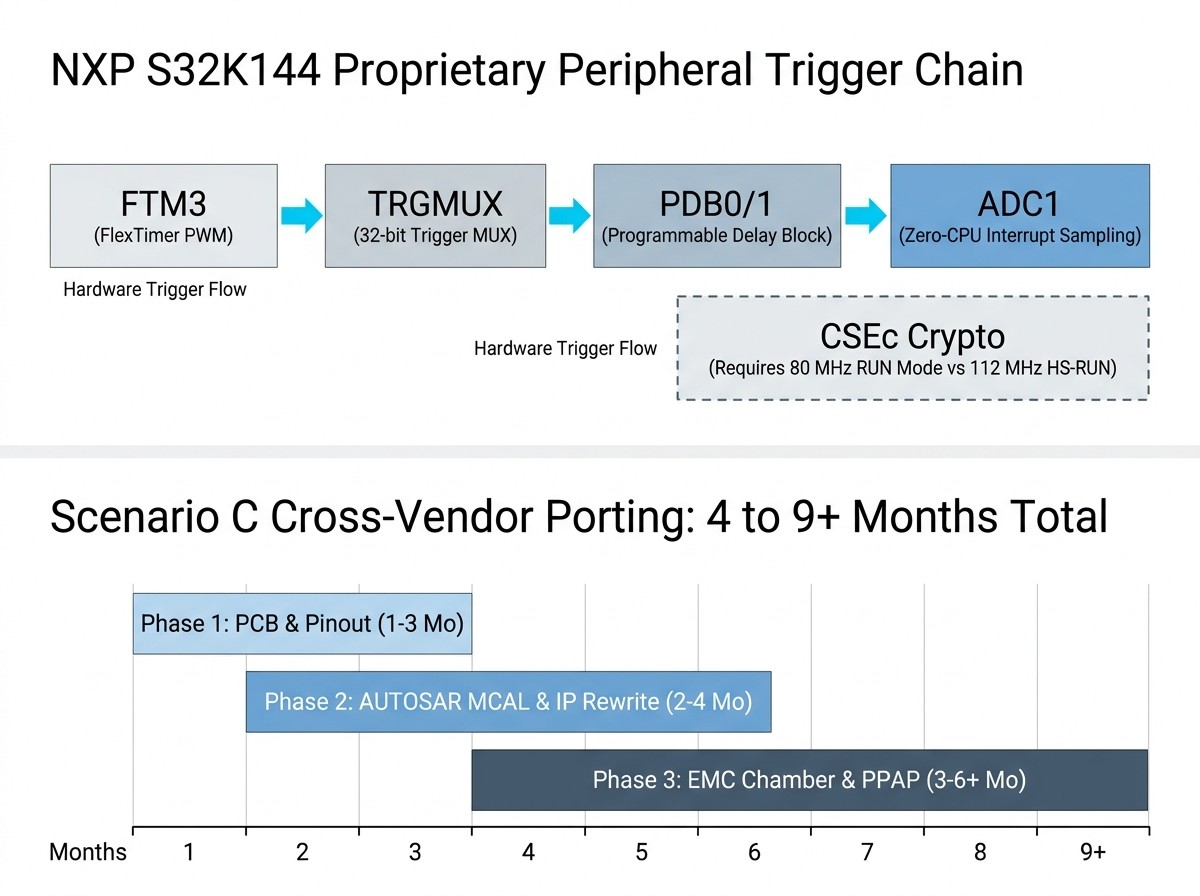
3. Firmware Porting: The 5-Pillar Automotive Ecosystem & AUTOSAR MCAL Friction
Qualitative procurement and engineering frameworks—such as the evaluation criteria summarized by The Insight Partners—emphasize that buyers must assess functional safety evidence, lifecycle support, software ecosystem maturity, cybersecurity features, and supply continuity. In practice, migrating automotive firmware across vendors requires rebuilding five distinct ecosystem pillars:
AUTOSAR MCAL (Microcontroller Abstraction Layer) & GUI Toolchains: Production automotive software rarely accesses hardware registers via simple hand-written C drivers. Instead, teams use vendor-specific GUI configuration tools to generate licensed AUTOSAR MCAL drivers. Switching MCU vendors requires licensing, configuring, and validating an entirely new vendor MCAL package and re-mapping upper-layer Basic Software (BSW) interfaces.
ISO 26262 Functional Safety Hardware IPs: Maintaining ASIL-B or ASIL-D compliance requires re-integrating vendor-specific safety manuals, lockstep CPU core diagnostics, Error-Correcting Code (ECC) memory fault handlers, Logic/Memory Built-In Self-Test (LBIST/MBIST) startup routines, and proprietary safety software libraries (such as SafeTlib).
HSM and SHE Hardware Cryptography: Secure boot, immobilizer key storage, and Secure Onboard Communication (SecOC) MAC verification rely on dedicated crypto co-processors (such as NXP's SHE-compliant
CSEcor dedicated 32-bit HSM cores on AURIX and Stellar). Porting requires rewriting asynchronous crypto driver calls and factory key-injection workflows.MATLAB Model-Based Design (MBD) Toolboxes: Control algorithms for battery management, inverters, and stability control are frequently auto-generated from Simulink using vendor-specific MATLAB MBD Target Support Packages. Migrating silicon requires swapping target blocks and running full Model-in-the-Loop (MIL) and Processor-in-the-Loop (PIL) regression suites.
Native Automotive Bus Validation: Re-verifying CAN-FD bit-timing, bus-off recovery behavior, LIN slave/master frame scheduling, and Ethernet Time-Sensitive Networking (TSN) buffers under worst-case bus loads.
4. Realistic Engineering & Qualification Timeline (Measured in Months)
Use the planning matrix below to set realistic expectations with executive leadership and OEM customers when evaluating a second-source MCU program.
Table 4: Second-Source MCU Qualification Timeline & Effort Estimate
Note: Durations represent indicative engineering planning ranges. Actual timelines depend on module ASIL criticality, bare-metal vs. full AUTOSAR architecture, and OEM customer PPAP review windows.
| Qualification Phase | Core Engineering & Compliance Deliverables | Scenario B: Same MPN, Alternate Fab/Assembly (Indicative) | Scenario C: Cross-Vendor / Family Redesign (Indicative) |
|---|---|---|---|
| Phase 1: Schematic, Pinout Audit & PCB Layout / Prototype Spin | Pin-multiplexing audit, power/clock simulation, bare-board layout, fab & SMT prototype assembly | 0 months (Drop-in footprint; no PCB artwork change) | ~1 to 3 months (Requires schematic update, layout, and proto build) |
| Phase 2: Bootloader, LLD / AUTOSAR MCAL Porting & HIL Regression | Flash wait-state tuning, peripheral IP (CAN-FD, TRGMUX/timers, HSM/CSEc) rewrite, ISO 26262 safety lib integration | ~0.5 to 1 month (Flash/timing sanity check & HIL regression) | ~2 to 4 months (Full MCAL configuration, driver rewrite & PIL/HIL testing) |
| Phase 3: Module EMC/EMI, Thermal Stress & OEM PPAP Sign-Off | Conducted/radiated emissions chamber testing, AEC-Q100 lot review, Part Submission Warrant (PSW) / PPAP approval | ~1 to 2 months (PCN equivalence review & customer delta-PPAP) | ~3 to 6+ months (Full EMC chamber scan, environmental stress & OEM PPAP) |
| Total End-to-End Calendar Impact | Concept Triage to Production Release | ~1.5 to 3 Months | ~4 to 9+ Months |
Late-October RFQ Checklist for 2027 Lock Windows (Including the Companion PMIC Trap)
Late October is the critical RFQ lock window where automotive Tier-1s and industrial OEMs finalize annual 2027 framework allocations. However, one of the most expensive procurement mistakes is locking wafer allocation on a 32-bit microcontroller while ignoring the companion Power Management IC (PMIC) or System Basis Chip (SBC) tied to the exact same power rail—creating a "golden screw" bottleneck that leaves allocated MCUs sitting idle in warehouse inventory.
Hidden Risk: The Companion PMIC & SBC Power-Rail Trap
High-safety 32-bit automotive MCUs do not run on generic, interchangeable single-rail voltage regulators. Instead, they pair with architected functional-safety PMICs that manage multi-rail power sequencing, precision ADC references, and hardware fail-safe state machines.
A classic production example is Infineon's OPTIREG TLF35584 (supplied in a PG-VQFN-48 package, ASIL-D and AEC-Q100 Grade 0/1 qualified), which is architected specifically as the companion power supply for AURIX TC2x/TC3x and Traveo microcontrollers. The TLF35584 integrates a wide 3.0 V to 40 V buck/boost pre-regulator with dedicated linear post-regulators for the MCU core and I/O (QUC at 5.0 V or 3.3 V / 600 mA), communication transceivers (QCO), and a precisionADC voltage reference (QVR). Crucially, it binds directly to the MCU via a 16-bit SPI interface, configurable Window and Functional Watchdogs (WWD/FWD), hardware error pin monitoring (ERR), and dual Safe State Control (SSC) outputs.
Because the MCU's safety startup firmware actively handshakes with the TLF35584 watchdog and voltage monitors over SPI, you cannot substitute a standard buck regulator if the companion PMIC goes on allocation. Similar tight coupling exists between NXP S32K3 MCUs and FS26/FS85 safety SBCs, or Renesas RH850 MCUs and their dedicated companion power ICs. Before locking your 2027 MCU contracts, review our analysis of power rail bottlenecks in the MCU Power Management Availability Forecast 2026: Lead Time Risks and Alternatives and cross-reference multi-component BOM exposure in IoT Chips Lead Time 2026: Navigating MCU, PMIC, and Sensor Shortages.
The 5-Point Late-October 2027 RFQ Lock & Sourcing Verification Checklist
Run every critical microcontroller and power-rail line item through this five-point verification protocol before signing 2027 supply agreements:
Demand Written Factory Allocation vs. Nominal Portal Quotes: Do not accept a generic system lead time (such as "18 weeks" or "24 weeks") on an RFQ spreadsheet as a binding delivery promise. Require written confirmation from the manufacturer or franchise partner that your quarterly 2027 delivery schedule is backed by reserved wafer starts or dedicated franchise buffer pipelines.
Lock a Dual-AVL Strategy Before PCB Layout Freeze: For new 2027/2028 hardware designs, qualify both a primary and secondary MCU family—or incorporate 0-ohm pinout strapping options and modular hardware abstraction layers—before freezing PCB artwork and submitting initial PPAP tooling.
Audit and Decouple Single-Source Companion PMICs on the MCU Rail: Require simultaneous, matching 2027 written allocation for the companion safety PMIC or SBC (such as the
TLF35584alongside anAURIXMCU) within the same RFQ package. Where ASIL partitioning permits, evaluate whether non-safety rails can be decoupled using multi-source discrete buck regulators and external supervisor ICs.Pre-Approve Upward Temperature Grade and Packaging Suffix Alternates on the BOM: Authorize upward-compatible thermal grades (approving both Grade 1
-40°Cto+125°Cand Grade 0-40°Cto+150°Csuffixes) as well as tape-and-reel (TR) versus tray packaging variants directly inside your ERP/BOM system. Pre-approving these suffixes allows procurement to claim available authorized lots immediately without losing weeks to an internal Engineering Change Order (ECO).Enforce Strict Traceability, MSL, and Lifecycle Verification on Secondary Stock: When executing
Scenario A(sourcing across global B2B distribution channels to bridge an allocation gap), require complete manufacturer lot traceability, original Certificates of Conformance (CoC), date-code verification, Moisture Sensitivity Level (MSL) dry-pack inspection, and X-ray/decap anti-counterfeit testing, while verifying that the target MPN suffix remains in active lifecycle status rather than Not Recommended for New Designs (NRND).
Frequently Asked Questions (FAQ)
What is the realistic lead time for automotive MCUs heading into 2027?
Directional planning lead times in late 2026 range from 14 to 26 weeks for standard mature-node catalog MCUs, 26 to 40 weeks for mainstream automotive body and industrial control families, and 30 to 52+ weeks for constrained 28nm and 40nm eNVM safety and electrification MPNs. Always verify live quotes per exact MPN suffix.
Why do industrial buyers experience shortages when automotive MCUs go on allocation?
Industrial automation, motor control, and medical microcontrollers share the exact same mature 40nm, 90nm, 130nm, and 180nm foundry wafer lines and back-end LQFP/QFN assembly houses as automotive body and chassis controllers. When Tier-1 automotive NCNR contracts lock wafer starts, residual capacity tightens across shared industrial families like STM32 and RL78.
Can an industrial-grade MCU replace an AEC-Q100 MCU during a supply crunch?
No for series vehicle production. Downward substitution violates AEC-Q100 Rev J1 multi-lot stress testing (3 lots of 77 units with zero failures), IATF 16949, OEM PPAP rules, and ISO 26262 safety requirements, restricting industrial parts to bench/HIL prototyping. Conversely, industrial buyers can safely upward-substitute AEC-Q100 Grade 1 or Grade 2 parts at a BOM cost premium.
How many months does it take to qualify a second-source MCU from a different vendor?
Qualifying a cross-vendor automotive MCU (Scenario C) typically requires 4 to 9+ months. This timeline spans schematic and PCB layout updates (1–3 months), flash wait-state tuning, proprietary peripheral IP (TRGMUX, FTM, CAN-FD, HSM) and AUTOSAR MCAL driver porting (2–4 months), and module-level EMC/thermal re-testing plus OEM PPAP approval (3–6+ months).
Why should procurement audit PMICs when locking 2027 MCU RFQs?
Modern 32-bit automotive MCUs (such as Infineon AURIX, NXP S32K3, Renesas RH850, and ST Stellar) rely on companion safety PMICs—like the TLF35584—for multi-rail voltage sequencing, precision ADC references, and SPI-linked window watchdogs. If a single-source companion PMIC goes on allocation, PCB assembly halts even when the MCU is in stock.
Conclusion & Sourcing Next Steps with Utmel Electronic Components
Navigating automotive mcu lead time 2026 and locking reliable 2027 production schedules requires looking beneath macro industry averages to manage exact MPN package suffixes, dual-fab PCN pathways, companion safety PMIC rails, and multi-month AUTOSAR/driver portability constraints. Teams that pair early framework commitments with pre-qualified BOM suffix flexibility will insulate their production lines from mature-node spillover.
Whether your team is auditing late-October 2027 RFQ quotes, searching for authorized upward-compatible AEC-Q100 suffixes, or bridging an unexpected allocation gap on a critical microcontroller or companion PMIC, Utmel Electronic Components provides market-aware B2B distribution and procurement support. Explore Utmel's comprehensive microcontroller and power management catalog to check real-time MPN availability across STMicroelectronics, NXP, Infineon, Renesas, Texas Instruments, and Microchip, compare multi-tier lead-time options, and submit your BOM for traceable alternative sourcing support.
Sources and references used for this guide
What is AEC-Q100 and it's Specifications?
Source type: official support page
Used for: Defining AEC-Q100 part-qualification standards, stress-test structures, and temperature grades for automotive integrated circuits.
Caution: Vendor knowledge base article; verify exact qualification test reports per specific MPN.Second Quarter FY 2024 Quarterly Update
Source type: official company documentation
Used for: Supporting Infineon's scale and historical growth in the automotive microcontroller sector.
Caution: Official investor presentation; reflects historical FY24 corporate performance rather than live 2026 MPN lead times.AEC-Q100 Devices
Source type: official company documentation
Used for: Illustrating vendor-level AEC-Q100 qualification workflows for automotive control and programmable ICs.
Caution: Vendor solution documentation; not neutral comparative ranking evidence.What Engineers Need to Know Automotive-Qualified MCU
Source type: reputable professional source
Used for: Detailing engineering selection and substitution criteria for automotive MCUs, including processing speed and CAN/LIN network interfaces.
Caution: Technical selection guide; does not provide live factory allocation or quote commitments.Powering Reliability - Ensuring Automotive Quality beyond AEC-Q100/101
Source type: reputable professional source
Used for: Explaining why automotive semiconductor reliability requires system-level quality controls and testing beyond nominal datasheet specifications.
Caution: Trade publication engineering analysis; specific PPAP requirements vary by automotive OEM.Ensuring Automotive Quality beyond AEC Q100/101
Source type: reputable professional source
Used for: Corroborating zero-defect reliability and extended qualification requirements for automotive-grade components.
Caution: Engineering trade article; use alongside official AEC-Q100 standards documentation.The Road to AEC-Q100 Qualification
Source type: reputable professional source
Used for: Confirming that integrated circuits including microcontrollers (MCUs), sensors, and memory chips are governed by AEC-Q100 qualification standards.
Caution: Industry engineering blog; verify specific revision rules (such as Rev-J) against official AEC documentation.NXP, Infineon, Renesas, TI, ST stay top five for auto ICs
Source type: reputable professional source
Used for: Establishing NXP, Infineon, Renesas, Texas Instruments, and STMicroelectronics as the core top five automotive IC suppliers.
Caution: Historical industry revenue context; do not use as a 2026 market-share percentage claim.
 UTMEL

We are the professional distributor of electronic components, providing a large variety of products to save you a lot of time, effort, and cost with our efficient self-customized service. careful order preparation fast delivery service
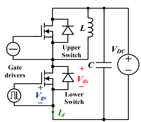 Discovering New and Advanced Methodology for Determining the Dynamic Characterization of Wide Bandgap DevicesSaumitra Jagdale15 March 20242924
For a long era, silicon has stood out as the primary material for fabricating electronic devices due to its affordability, moderate efficiency, and performance capabilities. Despite its widespread use, silicon faces several limitations that render it unsuitable for applications involving high power and elevated temperatures. As technological advancements continue and the industry demands enhanced efficiency from devices, these limitations become increasingly vivid. In the quest for electronic devices that are more potent, efficient, and compact, wide bandgap materials are emerging as a dominant player. Their superiority over silicon in crucial aspects such as efficiency, higher junction temperatures, power density, thinner drift regions, and faster switching speeds positions them as the preferred materials for the future of power electronics.
Read More Applications of FPGAs in Artificial Intelligence: A Comprehensive GuideUTMEL29 August 20255717
This comprehensive guide explores FPGAs as powerful AI accelerators that offer distinct advantages over traditional GPUs and CPUs. FPGAs provide reconfigurable hardware that can be customized for specific AI workloads, delivering superior energy efficiency, ultra-low latency, and deterministic performance—particularly valuable for edge AI applications. While GPUs excel at parallel processing for training, FPGAs shine in inference tasks through their adaptability and power optimization. The document covers practical implementation challenges, including development complexity and resource constraints, while highlighting solutions like High-Level Synthesis tools and vendor-specific AI development suites from Intel and AMD/Xilinx. Real-world applications span telecommunications, healthcare, autonomous vehicles, and financial services, demonstrating FPGAs' versatility in mission-critical systems requiring real-time processing and minimal power consumption.
Read More The 2026 Engineer’s Guide: Choosing the Right MCU for Your Next IoT & New Energy ProjectUTMEL30 April 20262125
A comprehensive comparison of 2026's leading MCUs from ST, NXP, and Microchip across power efficiency, processing performance, connectivity, and ecosystems to help engineers select the optimal chip for next-gen IoT and new energy projects.
Read More AI Server Components: Engineering Next-Gen Data Center Hardware for 100kW RacksUTMEL15 May 20261100
The transition from traditional enterprise IT to AI-driven workloads has rendered legacy data center hardware obsolete, forcing infrastructure planners to re-engineer server components for extreme thermal environments.
Read More The Practical Engineer’s Guide to the NE555N Timer: Pinout, Setup, and TroubleshootingUTMEL29 May 2026961
This comprehensive guide explores the NE555N timer, detailing its 8-pin layout, internal architecture, and key datasheet specifications. It compares the bipolar IC to CMOS variants and details setup configurations for astable, monostable, and bistable modes. Additionally, the guide offers practical troubleshooting advice to prevent common breadboard failures, such as floating reset pins and electrical noise issues.
Read More
Subscribe to Utmel !
![FM31L276-G]() FM31L276-G
Cypress Semiconductor Corp
![MCS3122T-I/ST]() MCS3122T-I/ST
Microchip Technology
![SI8230BB-D-IS]() SI8230BB-D-IS
Silicon Labs
![HCS365-I/SM]() HCS365-I/SM
Microchip Technology
![CAP014DG]() CAP014DG
Power Integrations
![FM31278-GTR]() FM31278-GTR
Cypress Semiconductor Corp
![ACNW3130-000E]() ACNW3130-000E
Broadcom Limited
![ACPL-3130-300E]() ACPL-3130-300E
Broadcom Limited
![HCS410/P]() HCS410/P
Microchip Technology
![L9654TR]() L9654TR
STMicroelectronics


