How to Design a High-precision ADC?

Tips on Improving ADC Measurement Accuracy and Resolution
Catalog |
1. What is ADC?
Essentially, the main difference between analog chips and digital chips is the difference in signal processing. As the name suggests, analog chips process analog signals, while digital chips process digital signals. The analog signal changes continuously over time, such as temperature, humidity, sound, speed, and so on. Their biggest feature is that there are countless different values within a certain time range.
In contrast, a digital signal is a bunch of discrete values, such as the binary 0101 used in computers. Since the transistor has two states of on and off, it can naturally represent the values of 0 and 1. There is no way for a transistor to achieve a state like 10% on or 31.5% off, so it is a digital signal.
In order to connect the two independent fields of analog and digital, it is necessary to use two kinds of chips as a bridge, one is the analog-to-digital conversion chip ADC, and the other is the digital-to-analog conversion chip DAC.
As the name implies, the analog-to-digital conversion chip ADC is used to convert analog signals into digital signals, and the analog-to-digital conversion DAC is just the other way round, converting digital signals into analog signals. However, in practical applications, ADC accounts for a higher proportion. Data shows that 80% of the applications where analog-to-digital conversion is applied are ADCs. Especially in the digital society, almost everything has been digitized, which is convenient for subsequent processing, transmission, and storage.
Many people may think that it is not difficult that the analog signal to be converted into a digital signal. In fact, the ADC is the most difficult analog chip. At the top conference ISSCC in the field of semiconductors and integrated circuits, that is, the International Solid-State Circuits Conference, there are quite a few articles on ADC design.
2. How to design and optimize ADC?
So, how exactly is the ADC implemented? Simply put, several processes such as sampling, quantization, and encoding are required. In other words, we first need to sample this signal and record the voltage value of the signal at regular intervals. The collected value will be quantized, converted into the corresponding digital signal value, and finally expressed by some kind of code, such as complement code, gray code, and so on.
ADC has many parameter indicators, of which there are two common parameters, one is ADC sampling rate or data rate, and the other is resolution. The sampling rate is well understood, that is, how many samplings can be done per unit time, and the more sampling points, the better the original signal can be restored.
Resolution is defined as the smallest change in the value of the input signal. This smallest change in value will change a code value of the ADC digital output value. In the case that the ADC has the same input range, the higher the resolution, the smaller the minimum change represented by a code value. If an ADC has 3 bits, then the entire voltage range can be divided into 2^3=8 parts. If the voltage range is 0-10V, then each part represents 1.25V. In other words, if the voltage change is less than this value, then the ADC cannot capture this small change. The important thing to note is that ADC resolution and ADC accuracy are two completely different concepts.

ADC code
There are many specific implementation forms of ADC, the common ones include successive approximation ADC (SAR), and there is also a Delta-Sigma ADC. For example, a common successive approximation ADC mainly integrates a voltage comparator, a register, a DAC, and some control circuits in the circuit. Its essence is to use binary search to determine the digital signal corresponding to the analog voltage. That is, in the beginning, the input voltage is compared with half of the reference voltage. If the input voltage is larger, then compare with three-quarters of the reference voltage. On the contrary, if the input voltage is smaller, it is compared with a quarter of the reference voltage. And so on, until the comparison is complete.
3. ADC drive design
However, even the most basic ADC is not simple in actual engineering applications, so supporting resource is particularly important. For example, ADCs often cannot work independently. They need to cooperate with other external circuits to function. One of the most important external circuits is the drive circuit.
As mentioned earlier, the ADC needs to sample, quantize and encode the input signal, and output an N-bit digital signal. These operations are usually completed in one cycle of the digital clock. This means that during the sampling process, the input signal should remain unchanged. This is a bit similar to the hold time of a clock in a digital signal.
Inside the ADC, its input actually contains a switch and a capacitor array, which is usually equivalent to a switch and a sampling capacitor. When the switch is closed, the capacitor is charged. After it is charged, the switch is opened, and the comparator and the DAC cooperate with each other to complete the sampling and quantization operation of the ADC at this time.
There are some problems. First of all, if the performance requirement of the ADC are relatively high. For example, if its sampling frequency is required to be high, then the time to charge the capacitor inside the ADC will be very short. If the sampling frequency is 1 million samples per second, then the charging time, that is, the capture time (TACQ) may only be 300 nanoseconds. If no circuit is added to the input as a driver, it will basically not be able to meet the demand for such a high sampling frequency. So in response to this problem, we usually add an operational amplifier to the ADC front end as a driver, so that sufficient charge can be provided to the sampling capacitor within a short sampling time.
This is not over yet. Although we can directly connect the op amp and ADC directly, we rarely design this way in practical applications. Because when the sampling frequency is very high, a very high bandwidth op amp is required if it is directly connected to the op amp. In addition, as can be seen from the simulation, the initial conversion may generate a large transient current when switching, and the driver circuit needs to be able to charge the ADC's internal sampling capacitor within a short ADC capture time (TACQ).
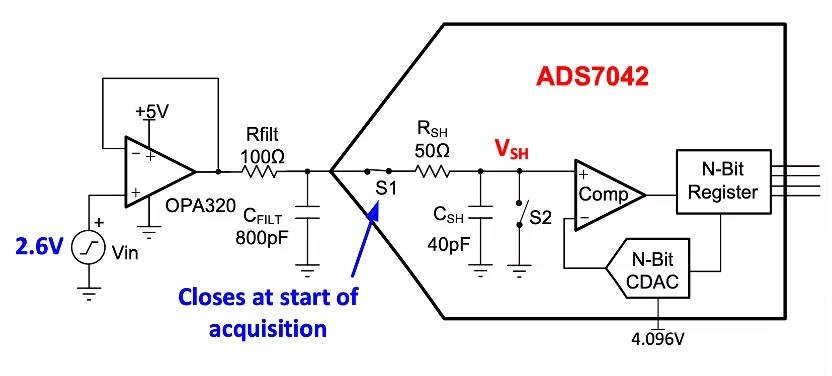
ADS7042 circuit
In order to meet these conditions and avoid large instantaneous currents, we can add an RC circuit before the ADC. We have learned in the university that the RC circuit is used for filtering, but its main function here is to use this extra capacitor to achieve faster charging. The op amp can fill this capacitor, and then when the ADC internal switch is closed, charge the ADC internal capacitor through this capacitor. Of course, in addition to this capacitor, part of the charge also comes from the front-end op amp. This RC circuit is also called a charge bucket filter circuit, which can effectively reduce the bandwidth requirements of the front-end op amp, so we can choose a lower bandwidth and lower cost ordinary op amp to meet the design needs. At the same time, it also eliminates the initial instantaneous current and greatly improves the stability of the circuit.
Here comes another question. How to determine the specific size and indicators of these amplifiers and RC circuits? There are two methods here, one is to derive through theoretical formulas, this is a very detailed derivation process on the Internet. According to the ADC indicators, such as resolution, sampling rate, reference voltage, etc., you can derive the required RC circuit and op-amp parameter data step by step.
Of course, there is another method, which is to perform simulation calculations through ready-made design tools and simulation tools. For example, Texas Instruments TI provides a series of related tools to simplify all the above calculation processes. In the beginning, you can select the corresponding device according to the performance indicators of the ADC, and then use the ADC SAR Drive tool to directly calculate the value of the resistance and capacitance, and get the corresponding performance indicators.
In order to further simplify the design process, TI not only provides design tools, but also a complete ecosystem to integrate these tools.

TI circuit cookbook
Taking SAR drive design as an example, TI provides many classic ADC circuit design solutions. For example, this "high-voltage battery monitor circuit" teaches us step by step from design description goals, to how to choose suitable devices, and how to model and simulate, and get the ideal performance index.
*This article was translated from: https://mp.weixin.qq.com/s/4r69kgCY5p1gOZnlEAd8CA
1. How does ADC convert analog to digital?
ADCs follow a sequence when converting analog signals to digital. They first sample the signal, then quantify it to determine the resolution of the signal, and finally set binary values and send it to the system to read the digital signal. Two important aspects of the ADC are its sampling rate and resolution.
2. How do you convert analog to digital?
If the two resistors are of equal values, that is R1 = R2, then clearly the reference voltage level will be equal to half the supply voltage, or V/2. So for a comparator with an open-collector output, if VIN is less than V/2, the output is HIGH, and if VIN is greater than V/2, the output is LOW acting as a 1-bit ADC.
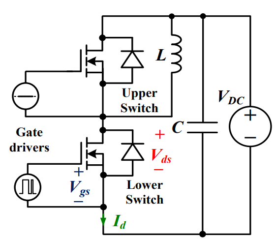 Discovering New and Advanced Methodology for Determining the Dynamic Characterization of Wide Bandgap DevicesSaumitra Jagdale15 March 20242471
For a long era, silicon has stood out as the primary material for fabricating electronic devices due to its affordability, moderate efficiency, and performance capabilities. Despite its widespread use, silicon faces several limitations that render it unsuitable for applications involving high power and elevated temperatures. As technological advancements continue and the industry demands enhanced efficiency from devices, these limitations become increasingly vivid. In the quest for electronic devices that are more potent, efficient, and compact, wide bandgap materials are emerging as a dominant player. Their superiority over silicon in crucial aspects such as efficiency, higher junction temperatures, power density, thinner drift regions, and faster switching speeds positions them as the preferred materials for the future of power electronics.
Read More A Comprehensive Guide to FPGA Development BoardsUTMEL11 September 202514692
This comprehensive guide will take you on a journey through the fascinating world of FPGA development boards. We’ll explore what they are, how they differ from microcontrollers, and most importantly, how to choose the perfect board for your needs. Whether you’re a seasoned engineer or a curious hobbyist, prepare to unlock new possibilities in hardware design and accelerate your projects. We’ll cover everything from budget-friendly options to specialized boards for image processing, delve into popular learning paths, and even provide insights into essential software like Vivado. By the end of this article, you’ll have a clear roadmap to navigate the FPGA landscape and make informed decisions for your next groundbreaking endeavor.
Read More Applications of FPGAs in Artificial Intelligence: A Comprehensive GuideUTMEL29 August 20253607
This comprehensive guide explores FPGAs as powerful AI accelerators that offer distinct advantages over traditional GPUs and CPUs. FPGAs provide reconfigurable hardware that can be customized for specific AI workloads, delivering superior energy efficiency, ultra-low latency, and deterministic performance—particularly valuable for edge AI applications. While GPUs excel at parallel processing for training, FPGAs shine in inference tasks through their adaptability and power optimization. The document covers practical implementation challenges, including development complexity and resource constraints, while highlighting solutions like High-Level Synthesis tools and vendor-specific AI development suites from Intel and AMD/Xilinx. Real-world applications span telecommunications, healthcare, autonomous vehicles, and financial services, demonstrating FPGAs' versatility in mission-critical systems requiring real-time processing and minimal power consumption.
Read More 800G Optical Transceivers: The Guide for AI Data CentersUTMEL24 December 20253835
The complete guide to 800G Optical Transceiver standards (QSFP-DD vs. OSFP). Overcome supply shortages and scale your AI data center with Utmel Electronic.
Read More Xilinx FPGAs: From Getting Started to Advanced Application DevelopmentUTMEL09 September 20254299
This guide is your comprehensive roadmap to understanding and mastering the world of Xilinx FPGA technology. From selecting your first board to deploying advanced AI applications, we'll cover everything you need to know to unlock the potential of these remarkable devices. The global FPGA market is on a significant growth trajectory, expected to expand from USD 8.37 billion in 2025 to USD 17.53 billion by 2035. This surge is fueled by the relentless demand for high-performance, adaptable computing in everything from 5G networks and data centers to autonomous vehicles and the Internet of Things (IoT). This guide will walk you through the key concepts, tools, and products in the Xilinx ecosystem, ensuring you're well-equipped to be a part of this technological revolution.
Read More
Subscribe to Utmel !
![UCC5310MCDR]() UCC5310MCDR
UCC5310MCDRTexas Instruments
![1EDI20H12AHXUMA1]() 1EDI20H12AHXUMA1
1EDI20H12AHXUMA1Infineon Technologies
![1EDI60H12AHXUMA1]() 1EDI60H12AHXUMA1
1EDI60H12AHXUMA1Infineon Technologies
![1EDI30I12MFXUMA1]() 1EDI30I12MFXUMA1
1EDI30I12MFXUMA1Infineon Technologies
![UCC21220DR]() UCC21220DR
UCC21220DRTexas Instruments
![HCS201T-I/SN]() HCS201T-I/SN
HCS201T-I/SNMicrochip Technology
![ADATE305BSVZ]() ADATE305BSVZ
ADATE305BSVZAnalog Devices Inc.
![AD9172BBPZ]() AD9172BBPZ
AD9172BBPZAnalog Devices Inc.
![ADUM4223CRWZ]() ADUM4223CRWZ
ADUM4223CRWZAnalog Devices Inc.
![FM33256B-G]() FM33256B-G
FM33256B-GCypress Semiconductor Corp


 Product
 Brand
Brand Articles
 Tools
Tools


