LDO vs Buck Converter: Which Power Regulator Is Best For Your Application?
Power management is a critical aspect of electronic design that directly impacts performance, efficiency, and battery life. Two commonly used voltage regulation technologies—Low Dropout Regulators (LDOs) and Buck Converters—serve similar purposes but operate on fundamentally different principles. Understanding when to use each can significantly optimize your design, reduce power consumption, and extend battery life in portable applications.
Whether you're designing wireless devices, embedded systems, or power-sensitive applications, choosing the right voltage regulator can make all the difference. This guide will help you navigate the complexities of LDOs and Buck Converters, comparing their efficiency, applications, and performance characteristics to help you make an informed decision.
Table of Contents
What is an LDO (Low Dropout Regulator)?
A Low Dropout Regulator (LDO) is a linear voltage regulator designed to operate with a minimal voltage difference between input and output. This voltage difference, known as the "dropout voltage," is typically much lower than conventional linear regulators—hence the name "low dropout."
LDOs use a pass transistor (either a PNP bipolar junction transistor or a P-channel MOSFET) operating in its saturation region to drop the excess voltage and provide a regulated output. This pass element acts like a variable resistor, continuously adjusting to maintain a constant output voltage regardless of load changes or input fluctuations.
Unlike traditional linear regulators that might require 2-3V of headroom between input and output, modern LDOs can operate with dropout voltages as low as 100-200mV. This makes them particularly valuable in battery-powered applications where every millivolt counts toward extending battery life.

The circuit architecture of a traditional LDO regulator showing the error amplifier, voltage reference, and pass transistor
Key LDO Characteristics:
Low noise output with minimal ripple
Simple circuit design with few external components
Compact form factor ideal for space-constrained designs
Good transient response to load changes
High Power Supply Rejection Ratio (PSRR) - ability to reject input noise
Low quiescent current for standby power efficiency
What is a Buck Converter?
A Buck Converter (also called a step-down converter) is a DC-to-DC power converter that efficiently reduces a higher input voltage to a lower regulated output voltage. Unlike linear regulators that dissipate excess voltage as heat, buck converters operate on switching principles to achieve much higher efficiency.
At its core, a buck converter works by rapidly switching the input voltage on and off using a semiconductor switch (typically a MOSFET), storing energy in an inductor during the "on" cycle, and releasing it during the "off" cycle. This switching approach allows the converter to transfer energy with minimal losses, achieving efficiency rates often exceeding 90%.
The output voltage is controlled by adjusting the duty cycle (ratio of on-time to the switching period) through feedback mechanisms. Modern buck converters typically operate at switching frequencies from hundreds of kHz to several MHz, allowing for smaller inductors and capacitors while maintaining high efficiency.
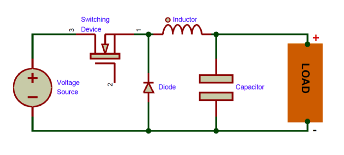
Basic circuit diagram of a buck converter showing the switch, diode, inductor, and output capacitor
Key Buck Converter Characteristics:
High efficiency, typically 80-95%, even with large input-to-output voltage differences
Requires more components (inductor, capacitors, control IC, MOSFETs)
Generates switching noise that may require filtering
Can handle higher power levels efficiently
More complex circuit design and PCB layout requirements
Available in both synchronous and non-synchronous configurations
Working Principles: How They Operate
LDO Operation Fundamentals
An LDO operates on a simple but effective principle of linear regulation. It consists of four main components:
Pass Element (Transistor): Acts as a variable resistor to control current flow
Error Amplifier: Compares the output voltage with a reference voltage
Voltage Reference: Provides a stable reference point
Feedback Network: Usually a resistor divider that samples the output voltage
The error amplifier continuously monitors the output voltage through the feedback network and compares it to the reference voltage. If the output voltage tries to change due to load or input variations, the error amplifier adjusts the conductivity of the pass element to maintain a constant output voltage.
For example, if the output voltage begins to drop, the error amplifier increases the drive to the pass transistor, allowing more current to flow and bringing the output voltage back up. Conversely, if the output voltage rises, the pass transistor conducts less, reducing the output voltage.
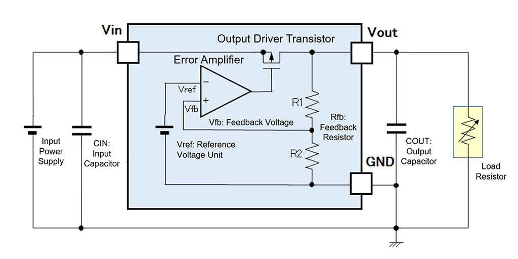
Working principle diagram of an LDO regulator showing the internal feedback loop
Buck Converter Operation Fundamentals
Buck converters operate based on energy storage and transfer principles using switchmode technology. The operation can be broken down into two main phases:
ON Phase (Charging): When the switch (MOSFET) is ON, the input voltage is applied across the inductor. Current flows through the inductor, which stores energy in its magnetic field while also supplying current to the load and charging the output capacitor.
OFF Phase (Discharging): When the switch turns OFF, the inductor's magnetic field collapses, creating a voltage that continues to push current through the circuit. This current flows through the diode (or lower MOSFET in synchronous designs), maintaining continuity while the inductor discharges its stored energy to the load.
By controlling the ratio of ON time to OFF time (the duty cycle), the converter regulates the output voltage. This PWM (Pulse Width Modulation) control is managed by a feedback loop that monitors the output voltage and adjusts the duty cycle as needed.
The relationship between input voltage (Vin), output voltage (Vout), and duty cycle (D) in a buck converter is approximated by: Vout = D × Vin
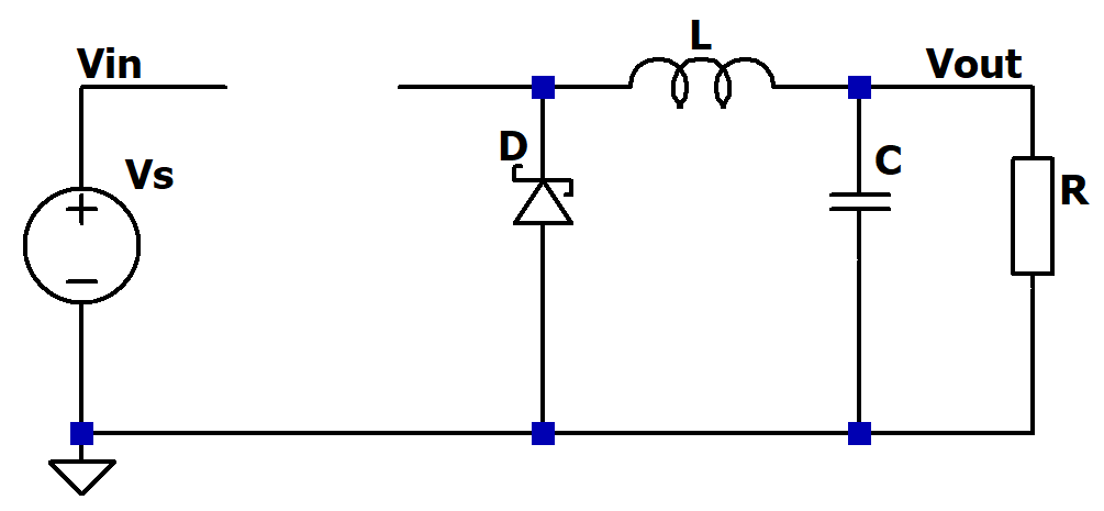
Buck converter operation showing current flow during switching cycles
LDO vs Buck Converter: Head-to-Head Comparison
| Characteristic | LDO Regulator | Buck Converter |
|---|---|---|
| Efficiency | Low to moderate (Vout/Vin × 100%); best when input-output differential is small | High (typically 80-95%) even with large input-output differentials |
| Heat Dissipation | High (excess voltage converted to heat) | Low (minimal power loss) |
| Noise/Ripple | Very low; clean output with high PSRR | Higher due to switching; requires filtering |
| Component Count | Minimal (typically just input/output capacitors) | Higher (inductor, capacitors, diode/MOSFET, controller) |
| PCB Footprint | Small | Larger (especially for higher power levels) |
| Cost | Lower | Higher |
| Transient Response | Excellent | Good, but typically slower than LDOs |
| EMI Generation | Minimal | Can be significant due to switching |
| Design Complexity | Simple | More complex (component selection, layout critical) |
| Power Handling | Limited by thermal considerations | Can handle high power efficiently |
Strengths of LDO Regulators
Ultra-Low Output Noise - Ideal for noise-sensitive analog circuits, RF applications, and precision measurement systems
Fast Transient Response - Responds quickly to load changes, making them suitable for applications with rapidly changing current demands
No Switching Noise - Absence of switching elements eliminates EMI concerns, simplifying system design
Simple Implementation - Minimal external components and straightforward design requirements make them easy to implement
Small Solution Size - Compact footprint makes them ideal for space-constrained designs
Improvement Areas for LDO Regulators
Limited Efficiency - Poor efficiency when input-output voltage differential is large
Thermal Management Challenges - Heat dissipation can be problematic in high-current applications
Power Limitations - Not practical for high-power applications due to thermal constraints
Strengths of Buck Converters
High Efficiency - Can achieve >90% efficiency even with large input-output voltage differentials
Excellent Power Handling - Capable of efficiently providing high current outputs
Minimal Heat Generation - Less thermal management required compared to linear solutions
Battery Life Extension - High efficiency translates directly to longer battery runtime in portable devices
Wide Input Voltage Range - Can accommodate broader input voltage variations while maintaining regulation
Improvement Areas for Buck Converters
Noise Generation - Switching noise can interfere with sensitive analog circuits
Design Complexity - Requires careful component selection and layout considerations
Larger Solution Size - Additional components result in larger footprint than LDOs
Efficiency Analysis: Power Loss vs Conversion Efficiency
LDO Efficiency
The efficiency of an LDO is directly proportional to the ratio of output voltage to input voltage:
η = (Vout / Vin) × 100%
For example, when converting 5V to 3.3V, the maximum theoretical efficiency is:
η = (3.3V / 5V) × 100% = 66%
This means that at least 34% of the input power is lost as heat, regardless of load current. The larger the voltage drop, the lower the efficiency. This is why LDOs are most efficient when the input and output voltages are close.
The power dissipation in an LDO can be calculated as:
Pdiss = (Vin - Vout) × Iout
Buck Converter Efficiency
Buck converters can maintain high efficiency regardless of the input-output voltage differential. Modern buck converters routinely achieve 85-95% efficiency across a wide range of input voltages and load conditions.
Power losses in buck converters come from several sources:
Switching losses in the MOSFETs
Conduction losses in the switches and inductor
Core losses in the inductor
Control circuit power consumption
ESR losses in capacitors
Despite these loss mechanisms, buck converters remain significantly more efficient than LDOs when there's a substantial difference between input and output voltages.
Efficiency Comparison Visualization

Efficiency comparison between LDO and buck converter across different input-output voltage differentials
Important Efficiency Considerations:
At very light loads, LDOs can sometimes be more efficient than buck converters due to the quiescent current of the buck converter's control circuitry
As load increases, buck converters quickly become more efficient than LDOs when there's a significant voltage difference
Modern buck converters employ various techniques like pulse skipping and burst mode to maintain efficiency at light loads
Thermal considerations often dictate the choice between LDO and buck converter, especially in high-current applications
"When considering efficiency, the key is to evaluate the entire operating range of your application. An LDO might be more efficient for very low power applications with small voltage differentials, while a buck converter almost always wins in higher power scenarios with larger voltage drops."
Common Applications and Use Cases
Typical LDO Applications
Noise-Sensitive Analog Circuits
RF front ends and transceivers
Audio amplifiers and DACs
Precision analog-to-digital converters
Phase-locked loops (PLLs)
Post-Regulation Scenarios
Filtering output noise from switching regulators
Creating multiple clean power rails from a single supply
Battery-Powered Devices (Low Dropout Needs)
Portable medical devices
Wearable technology
IoT sensors with small voltage differentials
Other Common Uses
Touch screens and display controllers
Camera modules
Reference voltage sources
Point-of-load regulation for processors
Typical Buck Converter Applications
Battery-Powered Systems (High Efficiency Needs)
Smartphones and tablets
Laptop computers
Portable power banks
Drones and RC vehicles
High Current Applications
CPU and GPU power supplies
Server power distribution
Automotive electronics
LED lighting systems
Large Voltage Differential Scenarios
12V to 3.3V/1.8V/1.2V conversions
24V industrial systems to logic-level voltages
Solar power systems
Other Common Uses
Point-of-load converters for FPGAs and ASICs
USB-powered devices
Telecommunication equipment
Industrial control systems
Combined Approach: Best of Both Worlds
In many modern designs, engineers combine both technologies to leverage their respective strengths:
Use a buck converter to efficiently step down from higher voltages (e.g., battery voltage to an intermediate level)
Follow with an LDO to create clean, noise-free power rails for sensitive analog circuits
This approach maximizes efficiency while ensuring noise-sensitive components receive clean power.
Selection Guide: When to Choose Which?
Selecting between an LDO and a buck converter depends on various factors related to your application requirements. The following decision tree and considerations will help guide your choice:
Choose an LDO When:
Your application requires minimal noise and high PSRR
The voltage differential (Vin-Vout) is small (typically<1V)
Current requirements are relatively low (<500mA)
Solution size and component count must be minimized
Design simplicity is a priority
The application involves sensitive analog circuits
Budget constraints favor lower component costs
EMI/RFI concerns must be minimized
Choose a Buck Converter When:
Efficiency is a primary concern
The voltage differential (Vin-Vout) is large (>1V)
Current requirements are high (>500mA)
Battery life must be maximized
Thermal management is a challenge
The application can tolerate some switching noise
Power dissipation must be minimized
The design requires handling higher power levels
Key Parameters to Consider
| Parameter | Considerations |
|---|---|
| Dropout Voltage | For LDOs, check the specified dropout voltage at your maximum load current. For battery-powered applications, ensure the LDO can maintain regulation as the battery discharges. |
| Quiescent Current | Critical for battery-powered devices in standby mode. Modern LDOs can achieve quiescent currents below 1µA, while buck converters typically have higher quiescent currents. |
| PSRR (Power Supply Rejection Ratio) | Higher PSRR means better rejection of input noise. Important for applications with dirty input power sources or noise-sensitive loads. |
| Load Transient Response | How quickly the regulator responds to sudden load changes. Critical for digital loads with rapidly changing current demands. |
| Output Noise | Measured in µVRMS, this indicates the noise generated by the regulator itself. LDOs typically produce less noise than buck converters. |
| Thermal Considerations | Calculate power dissipation and ensure adequate thermal management, especially for LDOs with high current and large voltage differentials. |
| Protection Features | Consider required protections: thermal shutdown, current limiting, short-circuit protection, reverse voltage protection, etc. |
Real-World Decision Example:
Scenario: Converting a Li-ion battery (3.7-4.2V) to power a 3.3V microcontroller and RF transceiver.
Analysis:
Voltage differential is small (0.4-0.9V) - Favors LDO
RF circuit requires low noise - Favors LDO
Battery life is important - Could favor buck converter
Space constraints exist - Favors LDO
Decision: In this case, an LDO would likely be the better choice due to the small voltage differential, noise sensitivity of the RF circuit, and space constraints. The efficiency advantage of a buck converter would be minimal with such a small voltage drop.
Product Recommendations
Based on performance, reliability, and application suitability, here are some recommended LDO regulators and buck converters for various design needs:
Recommended LDO Regulators
Texas Instruments TPS7A0233PYCHR
4-XFBGA, DSBGA Cut Tape Regulator IC
Ultra-low quiescent current (60 nA) LDO with fixed 3.3V output voltage, ideal for battery-powered applications requiring minimal power consumption in standby mode.
Key Specifications:
Input Voltage: Up to 6V
Output Current: 200mA
Dropout Voltage: 0.31V @ 200mA
Fixed 3.3V output
Protection: Over Current, Over Temperature, UVLO
Analog Devices LT3080EQ#TRPBF
TO-263-6 Adjustable Regulator IC
Adjustable LDO with wide output voltage range, excellent for applications requiring precise voltage adjustment and high power supply rejection ratio (PSRR).
Key Specifications:
Input Voltage: 1.2V - 36V
Adjustable Output: 0V - 36V
Dropout Voltage: 1.6V @ 1.1A
PSRR: 75dB ~ 20dB (120Hz ~ 1MHz)
Protection: Over Current, Over Temperature, Short Circuit
Recommended Buck Converters
Texas Instruments LM2596S-5.0/NOPB
TO-263-6 Switching Regulator IC
Simple Switcher® buck converter with fixed 5V output, offering high efficiency and ease of use for a wide range of applications requiring moderate current capabilities.
Key Specifications:
Input Voltage: 4.5V - 40V
Fixed 5V Output
Output Current: Up to 3A
Switching Frequency: 150kHz
Efficiency: Typically 80%
Analog Devices LTC3605IUF#TRPBF
24-WFQFN Switching Regulator IC
High-performance synchronous buck converter with high efficiency and fast transient response, ideal for applications requiring precise regulation and high efficiency across wide load ranges.
Key Specifications:
Input Voltage: 4V - 15V
Adjustable Output: 0.6V - 14.9V
Switching Frequency: 1MHz
Efficiency: Up to 96%
Synchronous Rectification
Selection Tips:
For battery-powered IoT devices: Consider ultra-low quiescent current LDOs like the TPS7A0233
For high-current applications: Buck converters like the LTC3605 offer better thermal performance
For analog/RF circuits: LDOs provide cleaner power with less filtering required
For industrial applications: Look for wide temperature range and robust protection features
For portable devices: Consider combination solutions with buck converters feeding LDOs
Frequently Asked Questions
Q: When can an LDO be more efficient than a buck converter?
An LDO can be more efficient than a buck converter in specific scenarios:
When the input-to-output voltage differential is very small (typically<0.5V)
At extremely light loads where the quiescent current of the buck converter's control circuitry becomes significant
In applications where the load current is very low and intermittent
In these cases, the power lost in the LDO can be less than the combined switching losses, control circuit power, and quiescent current of a buck converter.
Q: How do I calculate the power dissipation in an LDO to ensure proper thermal management?
Power dissipation in an LDO can be calculated using the formula:
Pdiss = (Vin - Vout) × Iout + (Vin × Iq)
Where:
Pdiss = Power dissipation in watts
Vin = Input voltage
Vout = Output voltage
Iout = Output current
Iq = Quiescent current of the LDO
For most applications, the quiescent current term is much smaller than the main dissipation term and can often be ignored for quick calculations. Once you know the power dissipation, you can determine the required thermal solution using the junction-to-ambient thermal resistance (θJA) of your package:
Tjunction = Tambient + (Pdiss × θJA)
Ensure that Tjunction stays below the maximum rated junction temperature of the device (typically 125°C or 150°C).
Q: What causes switching noise in buck converters and how can I mitigate it?
Switching noise in buck converters is primarily caused by the rapid switching of MOSFETs, inductor current ripple, and parasitic elements in the circuit. This noise manifests as voltage ripple on the output and potential EMI/RFI emissions.
To mitigate switching noise:
Use proper PCB layout techniques with short, direct traces and ground planes
Add input and output filtering capacitors with low ESR
Consider adding a small LC filter at the output for sensitive applications
Use an LDO post-regulator for extremely noise-sensitive circuits
Select buck converters with higher switching frequencies to reduce inductor and capacitor sizes
Implement EMI shielding for particularly sensitive designs
Follow manufacturer's layout guidelines and reference designs
Q: Can I use multiple LDOs in series for larger voltage drops while maintaining efficiency?
While technically possible, using multiple LDOs in series is generally not recommended for improving efficiency with large voltage drops. Each LDO in the chain will still dissipate power according to the voltage drop across it and the current flowing through it. The overall efficiency would be the product of the individual efficiencies, which doesn't improve the fundamental efficiency limitation of linear regulators.
A better approach for handling large voltage differentials is to:
Use a buck converter to efficiently step down to an intermediate voltage
Follow with an LDO for final regulation and noise filtering
This hybrid approach gives you the efficiency benefits of a switching regulator with the low-noise performance of an LDO.
Q: How important is the PSRR specification when selecting an LDO for analog circuits?
PSRR (Power Supply Rejection Ratio) is extremely important when selecting an LDO for analog circuits, particularly for noise-sensitive applications like RF circuits, precision ADCs, and audio equipment. PSRR measures the LDO's ability to reject ripple and noise from the input source, preventing it from appearing at the output.
Key considerations regarding PSRR:
PSRR varies with frequency - check the datasheet for PSRR curves across frequency ranges relevant to your application
Higher PSRR values (expressed in dB) indicate better noise rejection
PSRR typically decreases at higher frequencies
For applications where the input power may have switching noise (e.g., when powered from a buck converter), look for LDOs with good PSRR at the switching frequency
Modern high-performance LDOs can achieve PSRR values of 60-80dB at low frequencies
For extremely noise-sensitive applications, consider adding additional input and output filtering to further improve noise performance.
Conclusion
Choosing between an LDO regulator and a buck converter isn't a matter of which technology is inherently "better," but rather which is more suitable for your specific application requirements. Each has distinct advantages and limitations that make them optimal for different scenarios.
When to Choose LDOs:
Noise-sensitive analog, RF, or audio applications
Simple designs with minimal component count
Small voltage differentials between input and output
Low to moderate current requirements
When EMI/RFI must be minimized
When to Choose Buck Converters:
High efficiency requirements with large voltage drops
Battery-powered applications needing maximum runtime
High current applications where thermal management is challenging
Systems that can tolerate or filter switching noise
When efficiency outweighs simplicity concerns
In modern electronic designs, it's increasingly common to see hybrid approaches that leverage the strengths of both technologies. A buck converter efficiently steps down higher voltages, while an LDO provides final regulation for noise-sensitive circuits. This combination delivers both efficiency and low noise.
As electronic devices continue to become more power-conscious and feature-rich, understanding the tradeoffs between these power regulation technologies becomes ever more critical. By carefully analyzing your application's requirements for efficiency, noise, space constraints, thermal considerations, and complexity, you can select the optimal solution for your design.
Further Learning Resources
Power Management Integrated Circuit (PMIC) Guide - Comprehensive overview of power management solutions
PMIC Basic Types and Applications Video - Visual explanations of various power management ICs
What is an LDO (Low Dropout Regulator)? - Detailed exploration of LDO technology
What power regulation challenges are you facing in your designs? Have you found creative ways to combine LDOs and buck converters? Share your experiences in the comments below!
Join the Discussion
Thought-Provoking Questions
Have you ever encountered a design situation where an LDO was more efficient than a buck converter? What were the specific conditions?
In your experience, what techniques have been most effective for reducing switching noise in buck converter designs?
How do you approach thermal management when using LDOs in higher current applications? Do you have any creative cooling solutions to share?
As battery technologies evolve, how do you see the landscape of power regulation changing in the next 5-10 years?
Real User Experiences
Michael T. - Embedded Systems Engineer
"In a recent IoT sensor design, I was struggling with battery life issues. Our initial design used an LDO to power the MCU and sensor from a coin cell battery. After calculations, I realized we were losing almost 40% of our battery capacity to LDO inefficiency. Switching to a high-efficiency buck converter with ultra-low quiescent current extended our battery life from 6 months to nearly 2 years!"
Sophia R. - RF Circuit Designer
"For a sensitive RF front-end design, I initially tried powering everything with a buck converter to maximize efficiency. Despite extensive filtering, we kept having noise issues affecting receiver sensitivity. Eventually, we implemented a hybrid approach: a buck converter to an intermediate voltage followed by ultra-low-noise LDOs for the sensitive analog sections. This gave us both efficiency and performance."
James L. - Portable Medical Device Developer
"We faced a challenging thermal management problem when using an LDO to power a 1A load with a significant voltage drop. PCB space was extremely limited, so we couldn't use a buck converter. Our solution was to implement a multi-layer thermal via array directly under the LDO to conduct heat to a ground plane that acted as a heat spreader. This reduced junction temperature by nearly 25°C and allowed us to maintain our compact form factor."
Common Misconceptions
Misconception: "LDOs are always inefficient compared to buck converters"
Reality: When the input-to-output voltage differential is small (less than 1V), LDOs can achieve efficiency comparable to buck converters, especially at light loads where the quiescent current of the buck converter becomes significant. Always calculate the actual efficiency for your specific voltage conditions.
Misconception: "Buck converters are too noisy for analog circuits"
Reality: While buck converters do generate switching noise, careful design practices including proper component selection, PCB layout, and output filtering can significantly reduce noise to acceptable levels for many analog applications. Modern buck converters with higher switching frequencies can also simplify filtering requirements.
Misconception: "LDOs don't need heat sinking"
Reality: LDOs can dissipate significant heat when handling large voltage differentials or high currents. Proper thermal management, including adequate copper areas, thermal vias, and sometimes external heat sinks, is essential for reliable operation in these conditions.
Checklist of Options: Finding Your Ideal Solution
Step 1: Define Your Requirements
Power Requirements
□ Input voltage range: _______V to _______V
□ Required output voltage: _______V
□ Maximum load current: _______mA
□ Typical load current: _______mA
□ Minimum acceptable efficiency: _______%
Performance Requirements
□ Maximum allowable output noise: _______mVpp
□ Required PSRR: _______dB at _______Hz
□ Maximum allowed quiescent current: _______µA
□ Transient response requirement: _______µs
□ EMI/RFI sensitivity concerns: □ High □ Medium □ Low
Step 2: Consider Design Constraints
Physical Constraints
□ Maximum allowed PCB area: _______mm²
□ Maximum component height: _______mm
□ Available layers for power routing: _______
□ Thermal constraints: □ Natural convection □ Forced air □ Heat sink possible
Project Constraints
□ Budget per unit target: $_______
□ Development timeline: □ Tight □ Normal □ Relaxed
□ Team experience with buck converters: □ High □ Medium □ Low
□ Regulatory requirements: □ EMC □ Safety □ Other:_______
Step 3: Solution Selection Guidelines
□ If Vin - Vout < 0.5V, consider an LDO for simplicity
□ If Vin - Vout > 1V AND current > 100mA, consider a buck converter for efficiency
□ If noise-sensitive analog circuits are present, consider either an LDO or a buck + LDO combination
□ If battery life is critical AND voltage differential is large, prioritize a buck converter
□ If space is extremely limited, evaluate integration options (PMIC) or higher frequency buck converters
□ If thermal management is difficult, avoid LDOs with high power dissipation
□ For optimal combination systems: buck converter efficiency × LDO efficiency should exceed standalone options
Need More Help?
This checklist provides a starting point for selecting between LDO and buck converter solutions. For complex systems or specialized requirements, consider consulting datasheets, application notes, or working with an experienced power management specialist to optimize your design.
Video Learning: Buck Converter Operation
This informative video provides a detailed explanation of how buck converters work, from basic principles to practical applications.
External Resources
 Discovering New and Advanced Methodology for Determining the Dynamic Characterization of Wide Bandgap DevicesSaumitra Jagdale15 March 20242465
For a long era, silicon has stood out as the primary material for fabricating electronic devices due to its affordability, moderate efficiency, and performance capabilities. Despite its widespread use, silicon faces several limitations that render it unsuitable for applications involving high power and elevated temperatures. As technological advancements continue and the industry demands enhanced efficiency from devices, these limitations become increasingly vivid. In the quest for electronic devices that are more potent, efficient, and compact, wide bandgap materials are emerging as a dominant player. Their superiority over silicon in crucial aspects such as efficiency, higher junction temperatures, power density, thinner drift regions, and faster switching speeds positions them as the preferred materials for the future of power electronics.
Read More A Comprehensive Guide to FPGA Development BoardsUTMEL11 September 202514382
This comprehensive guide will take you on a journey through the fascinating world of FPGA development boards. We’ll explore what they are, how they differ from microcontrollers, and most importantly, how to choose the perfect board for your needs. Whether you’re a seasoned engineer or a curious hobbyist, prepare to unlock new possibilities in hardware design and accelerate your projects. We’ll cover everything from budget-friendly options to specialized boards for image processing, delve into popular learning paths, and even provide insights into essential software like Vivado. By the end of this article, you’ll have a clear roadmap to navigate the FPGA landscape and make informed decisions for your next groundbreaking endeavor.
Read More Applications of FPGAs in Artificial Intelligence: A Comprehensive GuideUTMEL29 August 20253577
This comprehensive guide explores FPGAs as powerful AI accelerators that offer distinct advantages over traditional GPUs and CPUs. FPGAs provide reconfigurable hardware that can be customized for specific AI workloads, delivering superior energy efficiency, ultra-low latency, and deterministic performance—particularly valuable for edge AI applications. While GPUs excel at parallel processing for training, FPGAs shine in inference tasks through their adaptability and power optimization. The document covers practical implementation challenges, including development complexity and resource constraints, while highlighting solutions like High-Level Synthesis tools and vendor-specific AI development suites from Intel and AMD/Xilinx. Real-world applications span telecommunications, healthcare, autonomous vehicles, and financial services, demonstrating FPGAs' versatility in mission-critical systems requiring real-time processing and minimal power consumption.
Read More 800G Optical Transceivers: The Guide for AI Data CentersUTMEL24 December 20253691
The complete guide to 800G Optical Transceiver standards (QSFP-DD vs. OSFP). Overcome supply shortages and scale your AI data center with Utmel Electronic.
Read More Xilinx FPGAs: From Getting Started to Advanced Application DevelopmentUTMEL09 September 20254268
This guide is your comprehensive roadmap to understanding and mastering the world of Xilinx FPGA technology. From selecting your first board to deploying advanced AI applications, we'll cover everything you need to know to unlock the potential of these remarkable devices. The global FPGA market is on a significant growth trajectory, expected to expand from USD 8.37 billion in 2025 to USD 17.53 billion by 2035. This surge is fueled by the relentless demand for high-performance, adaptable computing in everything from 5G networks and data centers to autonomous vehicles and the Internet of Things (IoT). This guide will walk you through the key concepts, tools, and products in the Xilinx ecosystem, ensuring you're well-equipped to be a part of this technological revolution.
Read More
Subscribe to Utmel !
![ATAES132A-SHER-B]() ATAES132A-SHER-B
ATAES132A-SHER-BMicrochip Technology
![AD5560JBCZ]() AD5560JBCZ
AD5560JBCZAnalog Devices Inc.
![ATECC108A-SSHDA-B]() ATECC108A-SSHDA-B
ATECC108A-SSHDA-BMicrochip Technology
![AT88SC12816C-SU]() AT88SC12816C-SU
AT88SC12816C-SUMicrochip Technology
![DLPC6401ZFF]() DLPC6401ZFF
DLPC6401ZFFTexas Instruments
![DLPA3005DPFDR]() DLPA3005DPFDR
DLPA3005DPFDRTexas Instruments
![MOC3163M]() MOC3163M
MOC3163MON Semiconductor
![HCS512/P]() HCS512/P
HCS512/PMicrochip Technology
![ATAES132A-MAHER-S]() ATAES132A-MAHER-S
ATAES132A-MAHER-SMicrochip Technology
![SN74AVC6T622RGYR]() SN74AVC6T622RGYR
SN74AVC6T622RGYRTexas Instruments


 Product
 Brand
Brand Articles
 Tools
Tools


