
 Product
 Brand
Brand Articles
 Tools
Tools

Updated October 2025 | Original Publication: 2020
Abstract
The graphene transistor was brought to global attention by the 2010 Nobel Prize in Physics. In 2004, Professor Andre Geim and Sir Konstantin Novoselov at the University of Manchester in the United Kingdom first isolated graphene from graphite flakes using a remarkably simple method, for which they were jointly awarded the 2010 Nobel Prize in Physics.
Graphene is a two-dimensional crystal composed of carbon atoms arranged in a hexagonal lattice. This structure is exceptionally stable. As the number of connected carbon atoms increases, this two-dimensional plane expands. A single layer of graphene has a thickness of only one carbon atom—approximately 0.335 nanometers, which is about 1/200,000th the thickness of a human hair. To put this in perspective, a 1-millimeter thick sheet of graphite contains nearly 3 million layers of graphene. Graphene is the thinnest and strongest material ever measured and possesses remarkable properties, including extremely high specific surface area and exceptional electrical conductivity.
Content Overview
This article explores the foundational concepts of graphene transistors, their historical development, and the latest breakthroughs that are paving the way for their commercial use. We will cover the initial discovery, the remarkable properties of this semiconductor material, key research milestones, and the current state of the technology in 2025.
I. The Quest for the Smallest Transistor

Figure 1. Structure of a graphene transistor
For many years, the processing limit of silicon materials was a primary concern for the semiconductor industry. While it was once thought that creating stable products below a 10-nanometer process would be impossible due to physical constraints, the industry has since pushed far beyond that limit. By 2025, semiconductor manufacturers such as TSMC and Samsung have successfully commercialized 3-nanometer process nodes and are actively developing 2-nanometer technology. However, the spirit of Moore's Law—the doubling of transistor density approximately every two years—has evolved. Future advancements now depend on novel materials like graphene to deliver breakthroughs in speed, efficiency, and new functionalities.
The world's first transistor made from graphene, developed by the team of Professor Andre Geim and Dr. Konstantin Novoselov, was only one atom thick and approximately 50 atoms wide. As a novel semiconductor material, graphene has been a focal point of the scientific community. The initial graphene transistors were created by etching a channel on a single-layer graphite film with an electron beam. This process formed quantum dots, or "charge islands," which could store a logic state, functioning like a standard field-effect transistor (FET). The researchers demonstrated that by applying voltage, the conductivity of these quantum dots could be changed, enabling them to memorize the transistor's logic state.
II. A Magical Semiconductor Material
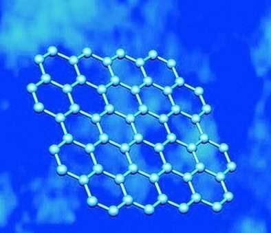
Figure 2. Graphene's hexagonal lattice structure
Dr. Novoselov once described graphene as a "gold mine" for research, and for over two decades, it has continued to yield new discoveries. Graphene is a single-atomic layer of graphite, a two-dimensional honeycomb crystal of carbon atoms. This unique structure gives it novel physical properties that distinguish it from bulk graphite. Graphene is a zero-bandgap semimetal with carrier mobility far exceeding that of silicon. Under ideal conditions, graphene can achieve electron mobility of up to 200,000 cm²/Vs, compared to silicon's approximately 1,400 cm²/Vs. Theoretically, its electron and hole mobility are equal, making its n-type and p-type field-effect transistors symmetrical.
The average free path of carriers in graphene can reach the micron level even at room temperature, making it a material with outstanding performance for electronics. Beyond transistors, graphene is used in composite materials, batteries, supercapacitors, hydrogen storage materials, field emission materials, and ultra-sensitive sensors. Researchers worldwide have invested significant effort in understanding how to prepare graphene and characterize its physical, chemical, and mechanical properties.
One reason for the intense interest in graphene was the prior research into carbon nanotubes. Graphene is likely to be a superior alternative to silicon for certain applications. In fact, carbon nanotubes are essentially graphene sheets rolled into cylindrical structures. Like carbon nanotubes, graphene has excellent electronic properties and can be used to make ultra-high-performance electronic products. What makes graphene more attractive than carbon nanotubes for many applications is that when making complex circuits, nanotubes must be carefully screened and positioned, whereas graphene, being a planar material, is more compatible with conventional fabrication techniques.
Silicon-based microcomputer processors can only perform a certain number of operations per second at room temperature. However, electrons pass through graphene with very little resistance, generating minimal heat. This, combined with graphene's excellent thermal conductivity, allows graphene-based electronics to operate at much higher speeds. While silicon device speeds are measured in gigahertz (GHz), graphene devices have the potential to operate at terahertz (THz) frequencies—a thousand times faster. As one expert noted, "The speed of silicon is limited; it can only reach a certain point and cannot be improved further." Computers made of graphene devices could theoretically run at terahertz speeds.
Beyond computing, graphene devices are being developed for communications and imaging technologies that require high-speed operation. Graphene is likely to be first applied in high-frequency fields, such as terahertz imaging, which has applications in security screening to detect hidden weapons. However, speed is not the only advantage of graphene. Silicon cannot be divided into small pieces smaller than a few nanometers without losing its attractive electronic properties. In contrast, graphene's fundamental physical properties remain stable even when it is patterned into structures just a few nanometers wide.
III. Foundational Research Milestones
Early experiments demonstrated graphene's remarkable properties. A team led by Professor Michael S. Fuhrer at the Center for Nanotechnology and Advanced Materials at the University of Maryland conducted pioneering experiments showing that graphene's electron mobility remained exceptionally high across a wide temperature range. They measured the electron mobility of graphene between 50 Kelvin and 500 Kelvin and found that regardless of temperature changes, the electron mobility was approximately 15,000 cm²/Vs. This is more than ten times higher than silicon's mobility of about 1,400 cm²/Vs. This confirmed that electrons travel much faster in graphene, positioning it as a potential successor to silicon for certain applications. The team also measured the thermal vibration effect of electron conduction in graphene for the first time, finding that it was very small.
In terms of mechanical strength, research has shown that graphene is the strongest material ever tested. Theoretical calculations by researchers Liu Fang and Li Ju at the Academy of Mathematics and Systems Science of the Chinese Academy of Sciences predicted an ideal tensile strength of 110-121 GPa for graphene. This means that graphene is extraordinarily strong relative to its weight.
Experimental work by James Hone and Jeffrey Kysar's group at Columbia University, published in the journal Science in July 2008, confirmed these predictions. They found that before graphene sample particles began to fragment, the maximum pressure they could withstand for every 100 nanometers was about 2.9 micronewtons. This result is equivalent to requiring a force of approximately 55 Newtons to break a 1-meter-long strip of graphene. If graphene with a thickness equivalent to a plastic food wrap (about 100 nanometers) could be made, it would require approximately 20,000 Newtons of force to tear it. While graphene is often described as "harder than diamond," it is more accurate to say it has a much higher tensile strength. Hardness, which measures resistance to indentation, is a more complex property for a two-dimensional material.
Published in Science magazine on September 26, 2008, research by Cai Weiwei, a Ph.D. student in the Solid State Quantum Information Laboratory of the Institute of Physics of the Chinese Academy of Sciences, under the guidance of researcher Chen Dongmin and Professor Rodney Ruoff, successfully synthesized high-quality 13C isotopically labeled graphite. This 13C-graphite was further dissociated into 13C-graphene and its derivative 13C-graphene oxide. Analysis of this material revealed the long-controversial chemical structure of graphene oxide, providing important insights for future applications.
IV. From Lab to Fabrication: The Evolution of Graphene Transistors
The journey from discovery to a viable product has been long, marked by key milestones. In March 2008, scientists at the IBM Watson Research Center created the first low-noise graphene transistors in the world, demonstrating the material's potential for practical electronic applications.
In May 2008, Professor Walt de Heer at the Georgia Institute of Technology, in collaboration with MIT's Lincoln Laboratory, successfully generated hundreds of graphene transistor arrays on a single chip. This achievement demonstrated the feasibility of large-scale integration of graphene devices.
At the end of June 2008, Professor Mitsugu Yamaguchi at the Research Institute of Electrical Communication at Tohoku University in Japan generated a single-layer graphite film (graphene) on a silicon substrate. This approach enabled high-speed device operation without requiring further miniaturization. For example, it could be used to make devices operating at 1012 Hz (terahertz) frequencies and ultra-high-performance microprocessors. Single-layer graphite films are difficult to produce and must have a honeycomb graphite structure with a thickness of only one carbon atom. Professor Yamaguchi's team controlled the crystalline direction during silicon carbide formation and the cutting direction of the silicon substrate to obtain a two-layer graphite film with an area of 100 × 150 square micrometers. Other research teams using traditional methods had lattice distortion rates of 20%, making them unsuitable for practical devices. Professor Yamaguchi's method involved heating the silicon carbide substrate to over 1,000 degrees Celsius under vacuum, removing silicon atoms, and allowing the remaining carbon to self-assemble into a single-layer graphite film.
A common misconception that arose during the early years of graphene research is that graphene is a superconductor. While standard graphene is an exceptional electrical conductor with very low resistance, it is not a superconductor under normal conditions. However, in 2018, researchers at MIT discovered that by twisting two layers of graphene to a specific "magic angle" (approximately 1.1 degrees) and cooling the system to near absolute zero temperatures, it could exhibit robust superconductivity. This field of "twistronics" has become a major area of ongoing research, but it is distinct from the properties of standard single-layer graphene used in most transistor applications.
V. The Commercial Revolution (2025 Update)
After nearly two decades of foundational research, the graphene transistor industry reached a pivotal turning point in 2024-2025. The most significant development came from a team led by Professor Walter de Heer at the Georgia Institute of Technology, who demonstrated the first functional graphene semiconductor with a proper band gap. This breakthrough, achieved by growing epitaxial graphene on silicon carbide substrates using specialized furnaces, solves the fundamental limitation that prevented graphene from being used in digital electronics. A band gap is essential for transistors to be switched fully "off," a requirement for digital logic circuits. This achievement delivers carrier mobility ten times greater than silicon while maintaining compatibility with conventional microelectronics processing.
This watershed moment has ignited commercial confidence and investment. In 2024, Black Semiconductor, a German startup, raised a record-breaking €254.4 million in Series A funding to develop graphene-based chip interconnects for data center applications. The German federal government and the state of North Rhine-Westphalia provided €228.7 million under the EU IPCEI Microelectronics program, while private equity led by Porsche Ventures contributed €25.7 million. This represents the largest funding round in graphene electronics history and signals a major shift from laboratory-scale research to industrial-scale production.
The market is now seeing its first commercial products. Graphenea, a leading graphene producer, has launched the world's first commercial graphene field-effect transistor (GFET) foundry service, producing 100 devices per day with projections to scale to 100,000 five-millimeter dies per day. Their GFET-S30 products feature 30 back-gated graphene transistor devices manufactured using proprietary High-K Metal Gate (HKMG) processes. Manufacturing yield improvements have been dramatic, with VTT Technical Research Centre and Graphenea demonstrating 99.9% device yield in wafer-scale CMOS integration—2,558 working devices out of 2,560 measured across five microchips.
The graphene electronics market, valued at over $1.2 billion in 2024, is projected to grow to $5.5 billion by 2033, representing an 18.5% compound annual growth rate. This growth is driven by applications where graphene's unique properties provide clear advantages over silicon.
Remarkable Physical Properties
| Property | Graphene | Silicon (for comparison) |
|---|---|---|
| Electron Mobility | Up to 200,000 cm²/Vs (ideal conditions) 10,000-70,000 cm²/Vs (practical devices) | ~1,400 cm²/Vs |
| Thickness | 0.335 nanometers (single atom layer) | N/A (bulk material) |
| Tensile Strength | 110-130 GPa | ~7 GPa |
| Specific Surface Area | 2,630 m²/g (theoretical) | N/A |
| Operating Frequency Potential | Terahertz (THz) range | Gigahertz (GHz) range |
| Energy Consumption (standby) | 100,000x lower than silicon | Baseline |
Key Application Areas
Biosensing represents the most advanced commercial application of graphene transistors. Graphene field-effect transistors have achieved single-molecule detection sensitivity that far exceeds conventional sensors. For example, multi-antibody graphene transistor sensors have been developed to detect SARS-CoV-2 in artificial saliva at concentrations as low as 3.5 × 10⁻¹⁷ g/mL. Clinical validation has shown 90.6% accuracy for COVID-19 detection in patient samples with response times under five minutes.
High-frequency electronics showcase graphene transistor advantages for next-generation communications. RF applications include frequency multipliers achieving 8.4% conversion efficiency for triplers operating at voltages below 1V, and terahertz switching capabilities several times faster than silicon-based devices. Cut-off frequencies up to 200 GHz have been demonstrated in laboratory settings.
Flexible electronics applications leverage graphene's mechanical properties to create bendable and wearable devices. Record-breaking flexible RF performance includes 39 GHz cut-off frequencies achieved on polymer substrates, while flexible graphene transistor devices maintain carrier mobility exceeding 2,500 cm²/Vs after 1,000 bending cycles.
Transparent conductive electrodes benefit from graphene's excellent electrical conductivity and light transmission properties. Touch screens, liquid crystal displays, organic photovoltaic cells, and organic light-emitting diodes all require good transparent conductive electrode materials. Graphene has better mechanical strength and flexibility than the commonly used material indium tin oxide (ITO). Large-area, continuous, transparent, high-conductivity graphene films can be made by chemical vapor deposition. These films have been used as anodes for photovoltaic devices, achieving energy conversion efficiencies of up to 1.71%, which represents approximately 55.2% of the efficiency of fabricated reference elements.
The Path Forward
The main production methods for graphene include micromechanical peeling (the original "scotch tape" method), epitaxial growth, graphite oxide reduction, and chemical vapor deposition (CVD). Among these, the graphite oxide reduction method is relatively low-cost and is one of the main methods for large-scale production. CVD has emerged as the preferred method for producing high-quality graphene for electronic applications.
Graphene's special structure makes it the thinnest and strongest material in the world, with exceptional toughness, electrical conductivity, and thermal conductivity. These special characteristics give it tremendous development potential, and it can be applied to a large number of fields such as electronics, aerospace, optics, energy storage, biomedicine, and daily life. As an emerging industry that has now transitioned from laboratory research to commercial production, the future of graphene is indeed bright. The convergence of scientific breakthroughs, manufacturing achievements, and commercial investments in 2024-2025 marks the beginning of the graphene electronics era.


