
 Product
 Brand
Brand Articles
 Tools
Tools
2N5458 JFET: Alternatives, Datasheet, Pinout


JFET N-CH 25V 0.31W TO92
This post will unlock more details about 2N5458, a TO-92 packaged N Channel JFET designed for switching and amplification requirements in general purpose applications.
2N5458 Pinout

2N5458 Pinout
2N5458 Description
The 2N5458 is an N−Channel Junction Field Effect Transistor, depletion mode (Type A) designed for audio and switching applications.
The transistor also possesses high gain and low noise feature which is very useful when amplifying a low gain signal and require high gain and low noise at the output. The drain and source of the transistor are swappable. The high input impedance feature and low noise capability also make it ideal to use this device for amplification purposes where the input signal is very low.
2N5458 CAD Model
Symbol

2N5458 Symbol
Footprint

2N5458 Footprint
3D Model

2N5458 3D Model
Specifications
- TypeParameter
- Lifecycle Status
Lifecycle Status refers to the current stage of an electronic component in its product life cycle, indicating whether it is active, obsolete, or transitioning between these states. An active status means the component is in production and available for purchase. An obsolete status indicates that the component is no longer being manufactured or supported, and manufacturers typically provide a limited time frame for support. Understanding the lifecycle status is crucial for design engineers to ensure continuity and reliability in their projects.
LAST SHIPMENTS (Last Updated: 1 week ago) - Mount
In electronic components, the term "Mount" typically refers to the method or process of physically attaching or fixing a component onto a circuit board or other electronic device. This can involve soldering, adhesive bonding, or other techniques to secure the component in place. The mounting process is crucial for ensuring proper electrical connections and mechanical stability within the electronic system. Different components may have specific mounting requirements based on their size, shape, and function, and manufacturers provide guidelines for proper mounting procedures to ensure optimal performance and reliability of the electronic device.
Through Hole - Mounting Type
The "Mounting Type" in electronic components refers to the method used to attach or connect a component to a circuit board or other substrate, such as through-hole, surface-mount, or panel mount.
Through Hole - Package / Case
refers to the protective housing that encases an electronic component, providing mechanical support, electrical connections, and thermal management.
TO-226-3, TO-92-3 (TO-226AA) - Number of Pins3
- Weight201mg
- Transistor Element Material
The "Transistor Element Material" parameter in electronic components refers to the material used to construct the transistor within the component. Transistors are semiconductor devices that amplify or switch electronic signals and are a fundamental building block in electronic circuits. The material used for the transistor element can significantly impact the performance and characteristics of the component. Common materials used for transistor elements include silicon, germanium, and gallium arsenide, each with its own unique properties and suitability for different applications. The choice of transistor element material is crucial in designing electronic components to meet specific performance requirements such as speed, power efficiency, and temperature tolerance.
SILICON - Breakdown Voltage / V25V
- Number of Elements1
- Operating Temperature
The operating temperature is the range of ambient temperature within which a power supply, or any other electrical equipment, operate in. This ranges from a minimum operating temperature, to a peak or maximum operating temperature, outside which, the power supply may fail.
135°C TJ - Packaging
Semiconductor package is a carrier / shell used to contain and cover one or more semiconductor components or integrated circuits. The material of the shell can be metal, plastic, glass or ceramic.
Bulk - Published2006
- JESD-609 Code
The "JESD-609 Code" in electronic components refers to a standardized marking code that indicates the lead-free solder composition and finish of electronic components for compliance with environmental regulations.
e0 - Pbfree Code
The "Pbfree Code" parameter in electronic components refers to the code or marking used to indicate that the component is lead-free. Lead (Pb) is a toxic substance that has been widely used in electronic components for many years, but due to environmental concerns, there has been a shift towards lead-free alternatives. The Pbfree Code helps manufacturers and users easily identify components that do not contain lead, ensuring compliance with regulations and promoting environmentally friendly practices. It is important to pay attention to the Pbfree Code when selecting electronic components to ensure they meet the necessary requirements for lead-free applications.
no - Part Status
Parts can have many statuses as they progress through the configuration, analysis, review, and approval stages.
Obsolete - Moisture Sensitivity Level (MSL)
Moisture Sensitivity Level (MSL) is a standardized rating that indicates the susceptibility of electronic components, particularly semiconductors, to moisture-induced damage during storage and the soldering process, defining the allowable exposure time to ambient conditions before they require special handling or baking to prevent failures
1 (Unlimited) - Number of Terminations3
- ECCN Code
An ECCN (Export Control Classification Number) is an alphanumeric code used by the U.S. Bureau of Industry and Security to identify and categorize electronic components and other dual-use items that may require an export license based on their technical characteristics and potential for military use.
EAR99 - Terminal Finish
Terminal Finish refers to the surface treatment applied to the terminals or leads of electronic components to enhance their performance and longevity. It can improve solderability, corrosion resistance, and overall reliability of the connection in electronic assemblies. Common finishes include nickel, gold, and tin, each possessing distinct properties suitable for various applications. The choice of terminal finish can significantly impact the durability and effectiveness of electronic devices.
Tin/Lead (Sn/Pb) - Additional Feature
Any Feature, including a modified Existing Feature, that is not an Existing Feature.
LOW NOISE - HTS Code
HTS (Harmonized Tariff Schedule) codes are product classification codes between 8-1 digits. The first six digits are an HS code, and the countries of import assign the subsequent digits to provide additional classification. U.S. HTS codes are 1 digits and are administered by the U.S. International Trade Commission.
8541.21.00.95 - Voltage - Rated DC
Voltage - Rated DC is a parameter that specifies the maximum direct current (DC) voltage that an electronic component can safely handle without being damaged. This rating is crucial for ensuring the proper functioning and longevity of the component in a circuit. Exceeding the rated DC voltage can lead to overheating, breakdown, or even permanent damage to the component. It is important to carefully consider this parameter when designing or selecting components for a circuit to prevent any potential issues related to voltage overload.
25V - Max Power Dissipation
The maximum power that the MOSFET can dissipate continuously under the specified thermal conditions.
625mW - Terminal Position
In electronic components, the term "Terminal Position" refers to the physical location of the connection points on the component where external electrical connections can be made. These connection points, known as terminals, are typically used to attach wires, leads, or other components to the main body of the electronic component. The terminal position is important for ensuring proper connectivity and functionality of the component within a circuit. It is often specified in technical datasheets or component specifications to help designers and engineers understand how to properly integrate the component into their circuit designs.
BOTTOM - Peak Reflow Temperature (Cel)
Peak Reflow Temperature (Cel) is a parameter that specifies the maximum temperature at which an electronic component can be exposed during the reflow soldering process. Reflow soldering is a common method used to attach electronic components to a circuit board. The Peak Reflow Temperature is crucial because it ensures that the component is not damaged or degraded during the soldering process. Exceeding the specified Peak Reflow Temperature can lead to issues such as component failure, reduced performance, or even permanent damage to the component. It is important for manufacturers and assemblers to adhere to the recommended Peak Reflow Temperature to ensure the reliability and functionality of the electronic components.
240 - Reach Compliance Code
Reach Compliance Code refers to a designation indicating that electronic components meet the requirements set by the Registration, Evaluation, Authorization, and Restriction of Chemicals (REACH) regulation in the European Union. It signifies that the manufacturer has assessed and managed the chemical substances within the components to ensure safety and environmental protection. This code is vital for compliance with regulations aimed at minimizing risks associated with hazardous substances in electronic products.
not_compliant - Current Rating
Current rating is the maximum current that a fuse will carry for an indefinite period without too much deterioration of the fuse element.
10mA - Time@Peak Reflow Temperature-Max (s)
Time@Peak Reflow Temperature-Max (s) refers to the maximum duration that an electronic component can be exposed to the peak reflow temperature during the soldering process, which is crucial for ensuring reliable solder joint formation without damaging the component.
30 - Base Part Number
The "Base Part Number" (BPN) in electronic components serves a similar purpose to the "Base Product Number." It refers to the primary identifier for a component that captures the essential characteristics shared by a group of similar components. The BPN provides a fundamental way to reference a family or series of components without specifying all the variations and specific details.
2N5458 - Pin Count
a count of all of the component leads (or pins)
3 - Qualification Status
An indicator of formal certification of qualifications.
Not Qualified - Element Configuration
The distribution of electrons of an atom or molecule (or other physical structure) in atomic or molecular orbitals.
Single - Operating Mode
A phase of operation during the operation and maintenance stages of the life cycle of a facility.
DEPLETION MODE - Power Dissipation
the process by which an electronic or electrical device produces heat (energy loss or waste) as an undesirable derivative of its primary action.
625mW - Power - Max
Power - Max is a parameter that specifies the maximum amount of power that an electronic component can handle without being damaged. It is typically measured in watts and indicates the upper limit of power that can be safely supplied to the component. Exceeding the maximum power rating can lead to overheating, malfunction, or permanent damage to the component. It is important to consider the power-max rating when designing circuits or systems to ensure proper operation and longevity of the electronic components.
310mW - FET Type
"FET Type" refers to the type of Field-Effect Transistor (FET) being used in an electronic component. FETs are three-terminal semiconductor devices that can be classified into different types based on their construction and operation. The main types of FETs include Metal-Oxide-Semiconductor FETs (MOSFETs), Junction FETs (JFETs), and Insulated-Gate Bipolar Transistors (IGBTs).Each type of FET has its own unique characteristics and applications. MOSFETs are commonly used in digital circuits due to their high input impedance and low power consumption. JFETs are often used in low-noise amplifiers and switching circuits. IGBTs combine the high input impedance of MOSFETs with the high current-carrying capability of bipolar transistors, making them suitable for high-power applications like motor control and power inverters.When selecting an electronic component, understanding the FET type is crucial as it determines the device's performance and suitability for a specific application. It is important to consider factors such as voltage ratings, current handling capabilities, switching speeds, and power dissipation when choosing the right FET type for a particular circuit design.
N-Channel - Transistor Application
In the context of electronic components, the parameter "Transistor Application" refers to the specific purpose or function for which a transistor is designed and used. Transistors are semiconductor devices that can amplify or switch electronic signals and are commonly used in various electronic circuits. The application of a transistor can vary widely depending on its design and characteristics, such as whether it is intended for audio amplification, digital logic, power control, or radio frequency applications. Understanding the transistor application is important for selecting the right type of transistor for a particular circuit or system to ensure optimal performance and functionality.
SWITCHING - Input Capacitance (Ciss) (Max) @ Vds
The parameter "Input Capacitance (Ciss) (Max) @ Vds" in electronic components refers to the maximum input capacitance measured at a specific drain-source voltage (Vds). Input capacitance is a crucial parameter in field-effect transistors (FETs) and power MOSFETs, as it represents the total capacitance at the input terminal of the device. This capacitance affects the device's switching speed and overall performance, as it influences the time required for charging and discharging during operation. Manufacturers provide this parameter to help designers understand the device's input characteristics and make informed decisions when integrating it into a circuit.
7pF @ 15V - Continuous Drain Current (ID)
Continuous Drain Current (ID) is a key parameter in electronic components, particularly in field-effect transistors (FETs) such as MOSFETs. It refers to the maximum current that can flow continuously through the drain terminal of the FET without causing damage to the component. This parameter is crucial for determining the power handling capability of the FET and is specified by the manufacturer in the component's datasheet. Designers must ensure that the actual operating current does not exceed the specified Continuous Drain Current to prevent overheating and potential failure of the component.
9mA - Gate to Source Voltage (Vgs)
The Gate to Source Voltage (Vgs) is a crucial parameter in electronic components, particularly in field-effect transistors (FETs) such as MOSFETs. It refers to the voltage difference between the gate and source terminals of the FET. This voltage determines the conductivity of the FET and controls the flow of current through the device. By varying the Vgs, the FET can be switched on or off, allowing for precise control of electronic circuits. Understanding and properly managing the Vgs is essential for ensuring the reliable and efficient operation of FET-based circuits.
3.5V - Drain to Source Breakdown Voltage
Drain to Source Breakdown Voltage, often denoted as V(BR) D-S, is a critical parameter in electronic components, particularly in field-effect transistors (FETs) and metal-oxide-semiconductor FETs (MOSFETs). It represents the maximum voltage that can be applied between the drain and source terminals of the device without causing breakdown or permanent damage. Exceeding this voltage can lead to excessive current flow, resulting in thermal failure or destruction of the component. It is essential for ensuring reliable operation in circuit designs where high voltages may be encountered.
25V - FET Technology
Field-Effect Transistor (FET) technology is a type of semiconductor device commonly used in electronic components such as transistors and integrated circuits. FETs operate by controlling the flow of current through a semiconductor channel using an electric field. There are several types of FETs, including Metal-Oxide-Semiconductor FETs (MOSFETs) and Junction FETs (JFETs), each with its own characteristics and applications. FET technology offers advantages such as high input impedance, low power consumption, and fast switching speeds, making it suitable for a wide range of electronic devices and circuits. Overall, FET technology plays a crucial role in modern electronics by enabling efficient and reliable signal processing and amplification.
JUNCTION - Current - Drain (Idss) @ Vds (Vgs=0)
The parameter "Current - Drain (Idss) @ Vds (Vgs=0)" in electronic components refers to the maximum drain current that flows through the device when the gate-source voltage (Vgs) is zero. This parameter is typically specified for field-effect transistors (FETs) and is an important characteristic that indicates the device's maximum current-carrying capacity in the off state. It helps in determining the saturation current of the FET and is crucial for designing circuits where high current handling capability is required. Manufacturers provide this parameter in the datasheet of the component to assist engineers and designers in selecting the appropriate component for their applications.
2mA @ 15V - Voltage - Cutoff (VGS off) @ Id
Voltage - Cutoff (VGS off) @ Id refers to the gate-source voltage at which a field-effect transistor (FET) or similar device ceases to conduct, effectively turning it off. This parameter indicates the threshold voltage that separates the conducting state from the cutoff state for a specified drain current (Id). It is crucial for determining the operating characteristics of the device in various applications, ensuring efficient switching and control in electronic circuits.
1V @ 10nA - REACH SVHC
The parameter "REACH SVHC" in electronic components refers to the compliance with the Registration, Evaluation, Authorization, and Restriction of Chemicals (REACH) regulation regarding Substances of Very High Concern (SVHC). SVHCs are substances that may have serious effects on human health or the environment, and their use is regulated under REACH to ensure their safe handling and minimize their impact.Manufacturers of electronic components need to declare if their products contain any SVHCs above a certain threshold concentration and provide information on the safe use of these substances. This information allows customers to make informed decisions about the potential risks associated with using the components and take appropriate measures to mitigate any hazards.Ensuring compliance with REACH SVHC requirements is essential for electronics manufacturers to meet regulatory standards, protect human health and the environment, and maintain transparency in their supply chain. It also demonstrates a commitment to sustainability and responsible manufacturing practices in the electronics industry.
No SVHC - RoHS Status
RoHS means “Restriction of Certain Hazardous Substances” in the “Hazardous Substances Directive” in electrical and electronic equipment.
Non-RoHS Compliant - Lead Free
Lead Free is a term used to describe electronic components that do not contain lead as part of their composition. Lead is a toxic material that can have harmful effects on human health and the environment, so the electronics industry has been moving towards lead-free components to reduce these risks. Lead-free components are typically made using alternative materials such as silver, copper, and tin. Manufacturers must comply with regulations such as the Restriction of Hazardous Substances (RoHS) directive to ensure that their products are lead-free and environmentally friendly.
Lead Free
2N5458 Feature
N-Channel for Higher Gain
Drain and Source Interchangeable
High AC Input Impedance
High DC Input Resistance
Low Transfer and Input Capacitance
Low Cross-Modulation and Intermodulation Distortion
Plastic Encapsulated Package
2N5458 Applications
Audio Preamplifier Applications
Audio Amplifier Stages
Low Level and Low Gain Signal Amplification
Sensor & Detector Circuits
2N5458 Alternatives
| Parts | Description | Manufacturer |
| 2N5458RL1 TRANSISTORS | Small Signal Field-Effect Transistor, 25V, 1-Element, N-Channel, Silicon, Junction FET, TO-92 | Motorola Semiconductor Products |
How to use 2N5458
The 2N5458 JFET can be used for a variety of signal amplification purposes for example it can be used in audio preamplifiers, audio amplifier stages and amplification of any small and low gain signal in electronics. On the other hand, it can also be used as a switch and is capable to drive a max load of up to 10mA.
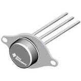
2N5458 Package

2N5458 Package
2N5458 Manufacturer
On Semiconductor (Nasdaq: ON) is a manufacturer engaging itself in reducing energy use. It features a comprehensive portfolio of power, signal management, and logic, custom solutions that are energy efficient. It acts as a world-class supply chain with high reliability and a network of manufacturing facilities, sales, offices, and design centres in key markets through North America, Europe, and the Asia Pacific regions.
Datasheet PDF
- PCN Obsolescence/ EOL :
- ReachStatement :
- Datasheets :
Popularity by Region
What are the types of JFET?
Furthermore, there are two major configurations of JFET, the N-Channel JFET, and the P-Channel JFET. The N-Channel JFET has better conductivity as compared to the P-Channel JFET as the electrons have higher mobility through a conductor.
What is 2N5458?
2N5457, 2N5458. JFETs - General Purpose. N−Channel − Depletion. N−Channel Junction Field Effect Transistors, depletion mode. (Type A) designed for audio and switching applications.
How does a JFET transistor work?
A JFET is a three-terminal semiconductor device in which current conduction is by one type of carrier i.e. electrons or holes. The current conduction is controlled by means of an electric field between the gate and the conducting channel of the device. The JFET has high input impedance and low noise levels.
Which is the equivalent of a 2n5458 transistor?
2N5457, 2N5459, NTE312, 2N5638, 2N5640, 2SK162, 2SK518 (Pin configuration of these equivalent or substitute transistors may different from 2N5458. It is important to check pin configuration before replacing in your circuit.)
 LF351 Op-Amp: Pinout, Circuit and Replacement
29 July 20215524
 STM8S003F3/K3 Microcontroller: A Comprehensive Technical Analysis
29 February 2024207
 NRF51822 Multiprotocol Bluetooth: Schematic, Pinout, and Datasheet
24 December 20215658
 74HC86 Exculsive or Gates : Pinout, Application and Datasheet
13 July 20216434
 MPS2222A Transistor:MPS2222A vs. 2N2222,MPS2222A Datasheet
14 March 20227501
![ATTINY45-20PU AVR series Microcontroller IC 8-Bit 20MHz[FAQ]: Datasheet, Features, and Pinout](https://res.utmel.com/Images/Article/a56c3c5f-b7ab-4a23-b644-a7088ffc38d8.jpg) ATTINY45-20PU AVR series Microcontroller IC 8-Bit 20MHz[FAQ]: Datasheet, Features, and Pinout
ATTINY45-20PU AVR series Microcontroller IC 8-Bit 20MHz[FAQ]: Datasheet, Features, and Pinout18 March 20221119
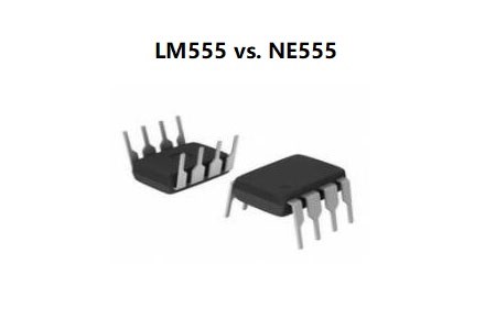 LM555 vs. NE555: What Difference is between LM555 and NE555?
13 March 202414806
 LM117H Voltage Regulator: Feature, Application, and Datasheet
04 June 20212005
 Graphics Card Explained: Classification, Working and Structure
27 May 202113573
 Capacitor Basic: How do Capacitors Work?
18 April 202515667
 How does the CPU recognize the Code?
08 August 20221164
 How to Pick the Perfect Boost Converter for Your Needs
07 June 20251118
 DoD Allocates $238 Million for Semiconductor Centers under CHIPS and Science Act
23 September 20232761
 Clock&Timing - Application Specific: A Dedicated Chip That Helps Produce Signals on the Circuit Board
22 February 20232101
 China to Inject $40 Billion into Semiconductor Sector with New State Fund
07 September 20232715
 Revolutionizing DC Link Bus Design: Unleashing High Frequency, High-Temperature Converter Potential
11 July 20233143
ON Semiconductor
In Stock: 14300
United States
China
Canada
Japan
Russia
Germany
United Kingdom
Singapore
Italy
Hong Kong(China)
Taiwan(China)
France
Korea
Mexico
Netherlands
Malaysia
Austria
Spain
Switzerland
Poland
Thailand
Vietnam
India
United Arab Emirates
Afghanistan
Åland Islands
Albania
Algeria
American Samoa
Andorra
Angola
Anguilla
Antigua & Barbuda
Argentina
Armenia
Aruba
Australia
Azerbaijan
Bahamas
Bahrain
Bangladesh
Barbados
Belarus
Belgium
Belize
Benin
Bermuda
Bhutan
Bolivia
Bonaire, Sint Eustatius and Saba
Bosnia & Herzegovina
Botswana
Brazil
British Indian Ocean Territory
British Virgin Islands
Brunei
Bulgaria
Burkina Faso
Burundi
Cabo Verde
Cambodia
Cameroon
Cayman Islands
Central African Republic
Chad
Chile
Christmas Island
Cocos (Keeling) Islands
Colombia
Comoros
Congo
Congo (DRC)
Cook Islands
Costa Rica
Côte d’Ivoire
Croatia
Cuba
Curaçao
Cyprus
Czechia
Denmark
Djibouti
Dominica
Dominican Republic
Ecuador
Egypt
El Salvador
Equatorial Guinea
Eritrea
Estonia
Eswatini
Ethiopia
Falkland Islands
Faroe Islands
Fiji
Finland
French Guiana
French Polynesia
Gabon
Gambia
Georgia
Ghana
Gibraltar
Greece
Greenland
Grenada
Guadeloupe
Guam
Guatemala
Guernsey
Guinea
Guinea-Bissau
Guyana
Haiti
Honduras
Hungary
Iceland
Indonesia
Iran
Iraq
Ireland
Isle of Man
Israel
Jamaica
Jersey
Jordan
Kazakhstan
Kenya
Kiribati
Kosovo
Kuwait
Kyrgyzstan
Laos
Latvia
Lebanon
Lesotho
Liberia
Libya
Liechtenstein
Lithuania
Luxembourg
Macao(China)
Madagascar
Malawi
Maldives
Mali
Malta
Marshall Islands
Martinique
Mauritania
Mauritius
Mayotte
Micronesia
Moldova
Monaco
Mongolia
Montenegro
Montserrat
Morocco
Mozambique
Myanmar
Namibia
Nauru
Nepal
New Caledonia
New Zealand
Nicaragua
Niger
Nigeria
Niue
Norfolk Island
North Korea
North Macedonia
Northern Mariana Islands
Norway
Oman
Pakistan
Palau
Palestinian Authority
Panama
Papua New Guinea
Paraguay
Peru
Philippines
Pitcairn Islands
Portugal
Puerto Rico
Qatar
Réunion
Romania
Rwanda
Samoa
San Marino
São Tomé & Príncipe
Saudi Arabia
Senegal
Serbia
Seychelles
Sierra Leone
Sint Maarten
Slovakia
Slovenia
Solomon Islands
Somalia
South Africa
South Sudan
Sri Lanka
St Helena, Ascension, Tristan da Cunha
St. Barthélemy
St. Kitts & Nevis
St. Lucia
St. Martin
St. Pierre & Miquelon
St. Vincent & Grenadines
Sudan
Suriname
Svalbard & Jan Mayen
Sweden
Syria
Tajikistan
Tanzania
Timor-Leste
Togo
Tokelau
Tonga
Trinidad & Tobago
Tunisia
Turkey
Turkmenistan
Turks & Caicos Islands
Tuvalu
U.S. Outlying Islands
U.S. Virgin Islands
Uganda
Ukraine
Uruguay
Uzbekistan
Vanuatu
Vatican City
Venezuela
Wallis & Futuna
Yemen
Zambia
Zimbabwe
![MMBFJ177LT1G]() MMBFJ177LT1G
MMBFJ177LT1GON Semiconductor
![MMBFJ201]() MMBFJ201
MMBFJ201ON Semiconductor
![MMBFJ108]() MMBFJ108
MMBFJ108ON Semiconductor
![MMBF4391LT1G]() MMBF4391LT1G
MMBF4391LT1GON Semiconductor
![MMBF4393LT1G]() MMBF4393LT1G
MMBF4393LT1GON Semiconductor
![MMBFJ175]() MMBFJ175
MMBFJ175ON Semiconductor
![MMBFJ175LT1G]() MMBFJ175LT1G
MMBFJ175LT1GON Semiconductor
![MMBF4392LT1G]() MMBF4392LT1G
MMBF4392LT1GON Semiconductor
![MMBFJ202]() MMBFJ202
MMBFJ202ON Semiconductor
![J175-D26Z]() J175-D26Z
J175-D26ZON Semiconductor


