
 Product
 Brand
Brand Articles
 Tools
Tools
74HC02 Quad 2-Input NOR Gate: 74HC02, Datasheet, Pinout

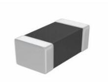
15 ns ns 7 ns ns 3mm mm Gates & Inverters 25mA mA Surface Mount Surface Mount 2V~6V V 2μA μA
Unit Price: $0.148713
Ext Price: $0.15


15 ns ns 7 ns ns 3mm mm Gates & Inverters 25mA mA Surface Mount Surface Mount 2V~6V V 2μA μA
The 74HC02 is a quad 2-input NOR gate. This article will unlock more details about 74HC02. There is a huge range of Semiconductors, Capacitors, Resistors and ICs in stock. Welcome RFQ!

7402 quad 2 input NOR gate integrated circuit 74HC02 quick look at electronics component
74HC02 Pinout

74HC02 Pinout
74HC02 CAD Model
Symbol

74HC02 Symbol
Footprint

74HC02 Footprint
CAD Model

74HC02 3D Model
74HC02 Description
The 74HC02 is a quad 2-input NOR gate. Inputs include clamp diodes. This enables the use of current limiting resistors to interface inputs to voltages in excess of VCC.
74HC02 Feature
• Wide supply voltage range from 2.0 V to 6.0 V
• CMOS low power dissipation
• High noise immunity
• Latch-up performance exceeds 100 mA per JESD 78 Class II Level B
• Input levels:
For 74HC02: CMOS level
For 74HCT02: TTL level
• Complies with JEDEC standards:
JESD8C (2.7 V to 3.6 V)
JESD7A (2.0 V to 6.0 V)
• ESD protection:
HBM JESD22-A114F exceeds 2000 V
MM JESD22-A115-A exceeds 200 V
• Multiple package options
• Specified from -40 °C to +85 °C and from -40 °C to +125 °C
Specifications
- TypeParameter
- Factory Lead Time8 Weeks
- Contact Plating
Contact plating (finish) provides corrosion protection for base metals and optimizes the mechanical and electrical properties of the contact interfaces.
Gold - Mount
In electronic components, the term "Mount" typically refers to the method or process of physically attaching or fixing a component onto a circuit board or other electronic device. This can involve soldering, adhesive bonding, or other techniques to secure the component in place. The mounting process is crucial for ensuring proper electrical connections and mechanical stability within the electronic system. Different components may have specific mounting requirements based on their size, shape, and function, and manufacturers provide guidelines for proper mounting procedures to ensure optimal performance and reliability of the electronic device.
Surface Mount - Mounting Type
The "Mounting Type" in electronic components refers to the method used to attach or connect a component to a circuit board or other substrate, such as through-hole, surface-mount, or panel mount.
Surface Mount - Package / Case
refers to the protective housing that encases an electronic component, providing mechanical support, electrical connections, and thermal management.
14-VFQFN Exposed Pad - Number of Pins14
- Logic Level-High1.5V ~ 4.2V
- Logic Level-Low0.5V ~ 1.8V
- Operating Temperature
The operating temperature is the range of ambient temperature within which a power supply, or any other electrical equipment, operate in. This ranges from a minimum operating temperature, to a peak or maximum operating temperature, outside which, the power supply may fail.
-40°C~125°C - Packaging
Semiconductor package is a carrier / shell used to contain and cover one or more semiconductor components or integrated circuits. The material of the shell can be metal, plastic, glass or ceramic.
Tape & Reel (TR) - Series
In electronic components, the "Series" refers to a group of products that share similar characteristics, designs, or functionalities, often produced by the same manufacturer. These components within a series typically have common specifications but may vary in terms of voltage, power, or packaging to meet different application needs. The series name helps identify and differentiate between various product lines within a manufacturer's catalog.
74HC - Published2013
- JESD-609 Code
The "JESD-609 Code" in electronic components refers to a standardized marking code that indicates the lead-free solder composition and finish of electronic components for compliance with environmental regulations.
e4 - Part Status
Parts can have many statuses as they progress through the configuration, analysis, review, and approval stages.
Active - Moisture Sensitivity Level (MSL)
Moisture Sensitivity Level (MSL) is a standardized rating that indicates the susceptibility of electronic components, particularly semiconductors, to moisture-induced damage during storage and the soldering process, defining the allowable exposure time to ambient conditions before they require special handling or baking to prevent failures
1 (Unlimited) - Number of Terminations14
- Max Power Dissipation
The maximum power that the MOSFET can dissipate continuously under the specified thermal conditions.
500mW - Voltage - Supply
Voltage - Supply refers to the range of voltage levels that an electronic component or circuit is designed to operate with. It indicates the minimum and maximum supply voltage that can be applied for the device to function properly. Providing supply voltages outside this range can lead to malfunction, damage, or reduced performance. This parameter is critical for ensuring compatibility between different components in a circuit.
2V~6V - Terminal Position
In electronic components, the term "Terminal Position" refers to the physical location of the connection points on the component where external electrical connections can be made. These connection points, known as terminals, are typically used to attach wires, leads, or other components to the main body of the electronic component. The terminal position is important for ensuring proper connectivity and functionality of the component within a circuit. It is often specified in technical datasheets or component specifications to help designers and engineers understand how to properly integrate the component into their circuit designs.
DUAL - Number of Functions4
- Supply Voltage
Supply voltage refers to the electrical potential difference provided to an electronic component or circuit. It is crucial for the proper operation of devices, as it powers their functions and determines performance characteristics. The supply voltage must be within specified limits to ensure reliability and prevent damage to components. Different electronic devices have specific supply voltage requirements, which can vary widely depending on their design and intended application.
5V - Terminal Pitch
The center distance from one pole to the next.
0.5mm - Base Part Number
The "Base Part Number" (BPN) in electronic components serves a similar purpose to the "Base Product Number." It refers to the primary identifier for a component that captures the essential characteristics shared by a group of similar components. The BPN provides a fundamental way to reference a family or series of components without specifying all the variations and specific details.
74HC02 - Pin Count
a count of all of the component leads (or pins)
14 - Number of Outputs1
- Output Voltage
Output voltage is a crucial parameter in electronic components that refers to the voltage level produced by the component as a result of its operation. It represents the electrical potential difference between the output terminal of the component and a reference point, typically ground. The output voltage is a key factor in determining the performance and functionality of the component, as it dictates the level of voltage that will be delivered to the connected circuit or load. It is often specified in datasheets and technical specifications to ensure compatibility and proper functioning within a given system.
6V - Operating Supply Voltage
The voltage level by which an electrical system is designated and to which certain operating characteristics of the system are related.
5V - Supply Voltage-Max (Vsup)
The parameter "Supply Voltage-Max (Vsup)" in electronic components refers to the maximum voltage that can be safely applied to the component without causing damage. It is an important specification to consider when designing or using electronic circuits to ensure the component operates within its safe operating limits. Exceeding the maximum supply voltage can lead to overheating, component failure, or even permanent damage. It is crucial to adhere to the specified maximum supply voltage to ensure the reliable and safe operation of the electronic component.
6V - Supply Voltage-Min (Vsup)
The parameter "Supply Voltage-Min (Vsup)" in electronic components refers to the minimum voltage level required for the component to operate within its specified performance range. This parameter indicates the lowest voltage that can be safely applied to the component without risking damage or malfunction. It is crucial to ensure that the supply voltage provided to the component meets or exceeds this minimum value to ensure proper functionality and reliability. Failure to adhere to the specified minimum supply voltage may result in erratic behavior, reduced performance, or even permanent damage to the component.
2V - Power Dissipation
the process by which an electronic or electrical device produces heat (energy loss or waste) as an undesirable derivative of its primary action.
500mW - Output Current
The rated output current is the maximum load current that a power supply can provide at a specified ambient temperature. A power supply can never provide more current that it's rated output current unless there is a fault, such as short circuit at the load.
25mA - Propagation Delay
the flight time of packets over the transmission link and is limited by the speed of light.
15 ns - Quiescent Current
The quiescent current is defined as the current level in the amplifier when it is producing an output of zero.
2μA - Turn On Delay Time
Turn-on delay, td(on), is the time taken to charge the input capacitance of the device before drain current conduction can start.
7 ns - Family
In electronic components, the parameter "Family" typically refers to a categorization or classification system used to group similar components together based on their characteristics, functions, or applications. This classification helps users easily identify and select components that meet their specific requirements. The "Family" parameter can include various subcategories such as resistors, capacitors, diodes, transistors, integrated circuits, and more. Understanding the "Family" of an electronic component can provide valuable information about its compatibility, performance specifications, and potential uses within a circuit or system. It is important to consider the "Family" parameter when designing or troubleshooting electronic circuits to ensure proper functionality and compatibility with other components.
HC/UH - Logic Function
In electronic components, the term "Logic Function" refers to the specific operation or behavior of a component based on its input signals. It describes how the component processes the input signals to produce the desired output. Logic functions are fundamental to digital circuits and are used to perform logical operations such as AND, OR, NOT, and XOR.Each electronic component, such as logic gates or flip-flops, is designed to perform a specific logic function based on its internal circuitry. By understanding the logic function of a component, engineers can design and analyze complex digital systems to ensure proper functionality and performance. Different logic functions can be combined to create more complex operations, allowing for the creation of sophisticated digital devices and systems.
NOR - Number of Inputs2
- Logic Type
Logic Type in electronic components refers to the classification of circuits based on the logical operations they perform. It includes types such as AND, OR, NOT, NAND, NOR, XOR, and XNOR, each defining the relationship between binary inputs and outputs. The logic type determines how the inputs affect the output state based on specific rules of Boolean algebra. This classification is crucial for designing digital circuits and systems, enabling engineers to select appropriate components for desired functionalities.
NOR Gate - Number of Gates
The number of gates per IC varies depending on the number of inputs per gate. Two?input gates are common, but if only a single input is required, such as in the 744 NOT(or inverter) gates, a 14 pin IC can accommodate 6 (or Hex) gates.
4 - Max Propagation Delay @ V, Max CL
The parameter "Max Propagation Delay @ V, Max CL" in electronic components refers to the maximum amount of time it takes for a signal to propagate through the component from input to output when operating at a specific voltage (V) and driving a maximum specified load capacitance (CL). This parameter is crucial in determining the speed and performance of the component in a circuit. A shorter propagation delay indicates faster signal processing and better overall performance. Designers use this parameter to ensure that signals can be transmitted and received within the required timing constraints in their electronic systems.
15ns @ 6V, 50pF - Number of Input Lines8
- Length3mm
- Radiation Hardening
Radiation hardening is the process of making electronic components and circuits resistant to damage or malfunction caused by high levels of ionizing radiation, especially for environments in outer space (especially beyond the low Earth orbit), around nuclear reactors and particle accelerators, or during nuclear accidents or nuclear warfare.
No - RoHS Status
RoHS means “Restriction of Certain Hazardous Substances” in the “Hazardous Substances Directive” in electrical and electronic equipment.
ROHS3 Compliant - Lead Free
Lead Free is a term used to describe electronic components that do not contain lead as part of their composition. Lead is a toxic material that can have harmful effects on human health and the environment, so the electronics industry has been moving towards lead-free components to reduce these risks. Lead-free components are typically made using alternative materials such as silver, copper, and tin. Manufacturers must comply with regulations such as the Restriction of Hazardous Substances (RoHS) directive to ensure that their products are lead-free and environmentally friendly.
Lead Free
Parts with Similar Specs
- ImagePart NumberManufacturerPackage / CaseNumber of InputsNumber of PinsLogic FunctionPropagation DelaySupply VoltageQuiescent CurrentTechnologyView Compare
![74HC02BQ,115]()
74HC02BQ,115
14-VFQFN Exposed Pad
2
14
NOR
15 ns
5 V
2 μA
CMOS
![SN74HC02DE4]()
14-SOIC (0.209, 5.30mm Width)
2
14
NOR
15 ns
5 V
2 μA
CMOS
![SN74HC02DBR]()
14-SSOP (0.209, 5.30mm Width)
2
14
NOR
15 ns
5 V
2 μA
CMOS
![74HC02BQ-Q100,115]()
14-VFQFN Exposed Pad
2
14
NOR
15 ns
5 V
2 μA
CMOS
![SN74HC02NSR]()
SOIC
-
14
NOR
15 ns
5 V
2 μA
CMOS


74HC02 Functional Diagram

74HC02 Functional Diagram
74HC02 Test Circuit

74HC02 Test Circuit

74HC02 Waveforms
Datasheet PDF
- PCN Packaging :
- Datasheets :
- PCN Assembly/Origin :
- RohsStatement :
Trend Analysis
What is a 74hc02 gate?
The 74HC02; 74HCT02 is a quad 2-input NOR gate. Inputs include clamp diodes. This enables the use of current limiting resistors to interface inputs to voltages in excess of VCC.
Who owns the copyright of 74hc02 datasheet?
Note: The Copyright of this 74HC02 Datasheet belongs to Fairchild Semiconductor and is provided for information only.
When did the sn54hc02 scls076g come out?
SN74HC02, SN54HC02 SCLS076G – DECEMBER 1982 – REVISED DECEMBER 2020 An IMPORTANT NOTICE at the end of this data sheet addresses availability, warranty, changes, use in safety-critical applications, intellectual property matters and other important disclaimers.
What is NAND logic gate?
In digital electronics, a NAND gate (NOT-AND) is a logic gate that produces an output that is false only if all its inputs are true; thus its output is complemented to that of an AND gate. A LOW (0) output results only if all the inputs to the gate are HIGH (1); if any input is LOW (0), a HIGH (1) output results.
What is NAND operation?
The NAND operation is the basic logical operation performed by the solid-state transistors ("NAND gates") that underlie virtually all integrated circuits and modern computers. The first axiom system based on NAND was given by Henry Sheffer in 1913.What is the input and output voltage range of 74HC02 OR gate chip?
The 74HC series devices have a wide operating voltage range, which can work under a voltage of 2~6V. The range of input and output levels is different for different operating voltages.
 Detailed Features and Specifications of STM32F051C8T6
24 July 2025281
 Murata BLM18PG471SN1D: Datasheet, Application, and Alternatives
11 February 2022333
 LM1875T/NOPB Audio Amplifier: Feature,Specification,Datasheet
17 May 20214075
 32-bit ARM-Based Microcontrollers SAM D21E / SAM D21G /SAM D21J
29 February 2024103
![2N2907A Small Signal PNP Transistors: Pinout, Datasheet pdf and Equivalent [Video]](https://res.utmel.com/Images/Article/e3cebe8c-d535-40d4-af81-ca08b3da049a.jpg) 2N2907A Small Signal PNP Transistors: Pinout, Datasheet pdf and Equivalent [Video]
2N2907A Small Signal PNP Transistors: Pinout, Datasheet pdf and Equivalent [Video]15 December 20214674
![A23 Energizer A23 Batteries Miniature Alkaline 12V [Video]: Datasheet, Application, and Equivalents](https://res.utmel.com/Images/Article/f7ee8460-e4da-4af6-933b-454755320e46.jpg) A23 Energizer A23 Batteries Miniature Alkaline 12V [Video]: Datasheet, Application, and Equivalents
A23 Energizer A23 Batteries Miniature Alkaline 12V [Video]: Datasheet, Application, and Equivalents25 March 20223013
![Is LM317 better than LM7805?[video+FAQ]](https://res.utmel.com/Images/Article/5cafb24b-3f28-4935-b123-c59a0f9c15eb.jpg) Is LM317 better than LM7805?[video+FAQ]
Is LM317 better than LM7805?[video+FAQ]27 April 20228691
 SiM3C154B/GM 32-bit ARM Cortex-M3 Microcontroller: Technical Overview and Applications
29 February 2024164
 Good News: UTMEL Electronic is now the Authorized Distributor for Isocom Components 2004 Ltd.
10 November 20237912
 Introduction to EPROM and EEPROM
08 January 202614700
 How do Inductors Work?
27 October 202515639
 DIP Switch: Introduction and Classification
20 January 202115620
 What are the Applications of Filters?
17 January 202616131
 How to treat 5G?
23 October 20212285
 Introduction to Types of Motion Sensors
24 October 20259170
 What are Fiber Optic Patch Cables?
11 February 20227761
Nexperia USA Inc.
In Stock: 500
Minimum: 1 Multiples: 1
Qty
Unit Price
Ext Price
1
$0.148713
$0.15
10
$0.140296
$1.40
100
$0.132354
$13.24
500
$0.124863
$62.43
1000
$0.117795
$117.80
Not the price you want? Send RFQ Now and we'll contact you ASAP.
Inquire for More Quantity
![74HCT86D,653]() 74HCT86D,653
74HCT86D,653Nexperia USA Inc.
![74HC04D,653]() 74HC04D,653
74HC04D,653Nexperia USA Inc.
![74HC32D,653]() 74HC32D,653
74HC32D,653Nexperia USA Inc.
![74AHC1G32GW,125]() 74AHC1G32GW,125
74AHC1G32GW,125Nexperia USA Inc.
![HEF4093BT,653]() HEF4093BT,653
HEF4093BT,653Nexperia USA Inc.
![74HC02D,653]() 74HC02D,653
74HC02D,653Nexperia USA Inc.
![74LVC14APW,118]() 74LVC14APW,118
74LVC14APW,118Nexperia USA Inc.
![74AUP1G08GX,125]() 74AUP1G08GX,125
74AUP1G08GX,125Nexperia USA Inc.
![74LVC1G14GV,125]() 74LVC1G14GV,125
74LVC1G14GV,125Nexperia USA Inc.
![HEF4069UBT,653]() HEF4069UBT,653
HEF4069UBT,653Nexperia USA Inc.


