
 Product
 Brand
Brand Articles
 Tools
Tools
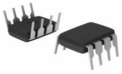
AT45DB081E 8-Mbit DataFlash: Pinout, Features and Datasheet

Surface Mount Memory IC 8 Mb kb 6mm mm 15mA mA 8b b
Unit Price: $1.783755
Ext Price: $1.78


Surface Mount Memory IC 8 Mb kb 6mm mm 15mA mA 8b b
The AT45DB081E is a 1.7V minimum, serial-interface sequential access Flash memory ideally suited for a wide variety of digital voice, image, program code, and data storage applications. The AT45DB081E also supports the RapidS serial interface for applications requiring very high speed operation. Furthermore, Huge range of Semiconductors, Capacitors, Resistors and IcS in stock. Welcome RFQ.
DataFlash Overview
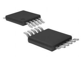
AT45DB081E Pinout
The following figure is the diagram of AT45DB081E Pinout.

Pinout
AT45DB081E CAD Model
The followings are AT45DB081E Symbol, Footprint, and 3D Model.

Symbol

Footprint

3D Model
AT45DB081E Description
The AT45DB081E is a 1.7V minimum, serial-interface sequential access Flash memory ideally suited for a wide variety of digital voice, image, program code, and data storage applications. The AT45DB081E also supports the RapidS serial interface for applications requiring very high speed operation. Its 8,650,752 bits of memory are organized as 4,096 pages of 256 bytes or 264 bytes each. In addition to the main memory, the AT45DB081E also contains two SRAM buffers of 256/264 bytes each. The buffers allow receiving of data while a page in the main memory is being reprogrammed.
To allow for simple in-system re-programmability, the AT45DB081E does not require high input voltages for programming. The device operates from a single 1.7V to 3.6V power supply for the erase and program and read operations. The AT45DB081E is enabled through the Chip Select pin and accessed via a 3-wire interface consisting of the Serial Input (SI), Serial Output (SO), and the Serial Clock (SCK). All programming and erase cycles are self-timed.
This article provides you with a basic overview of the AT45DB081E 8-Mbit DataFlash, including its pin descriptions, features and specifications, etc., to help you quickly understand what AT45DB081E is.
AT45DB081E Features
● Single 1.7V - 3.6V supply
● Serial Peripheral Interface (SPI) compatible
◆ Supports SPI modes 0 and 3
◆ Supports RapidS™ operation
● Continuous read capability through entire array
◆ Up to 85MHz
◆ Low-power read option up to 15MHz
◆ Clock-to-output time (tV) of 6ns maximum
● User configurable page size
◆ 256 bytes per page
◆ 264 bytes per page (default)
◆ Page size can be factory pre-configured for 256 bytes
● Two fully independent SRAM data buffers (256/264 bytes)
◆ Allows receiving data while reprogramming the main memory array
● Flexible programming options
◆ Byte/Page Program (1 to 256/264 bytes) directly into main memory
◆ Buffer Write
◆ Buffer to Main Memory Page Program
● Flexible erase options
◆ Page Erase (256/264 bytes)
◆ Block Erase (2KB)
◆ Sector Erase (64KB)
◆ Chip Erase (8-Mbits)
● Program and Erase Suspend/Resume
● Advanced hardware and software data protection features
◆ Individual sector protection
◆ Individual sector lockdown to make any sector permanently read-only
● 128-byte, One-Time Programmable (OTP) Security Register
◆ 64 bytes factory programmed with a unique identifier
◆ 64 bytes user programmable
● Hardware and software controlled reset options
● JEDEC Standard Manufacturer and Device ID Read
● Low-power dissipation
◆ 400nA Ultra-Deep Power-Down current (typical)
◆ 4.5µA Deep Power-Down current (typical)
◆ 25µA Standby current (typical)
◆ 11mA Active Read current (typical at 20MHz)
● Endurance: 100,000 program/erase cycles per page minimum
● Data retention: 20 years
● Complies with full industrial temperature range
● Green (Pb/Halide-free/RoHS compliant) packaging options
◆ 8-lead SOIC (0.150" wide and 0.208" wide)
◆ 8-pad Ultra-thin DFN (5 x 6 x 0.6mm)
◆ 8-ball (2 x4 Array) Wafer Level Chip Scale Package
◆ Die in Wafer Form
Specifications
- TypeParameter
- Factory Lead Time8 Weeks
- Contact Plating
Contact plating (finish) provides corrosion protection for base metals and optimizes the mechanical and electrical properties of the contact interfaces.
Gold - Mount
In electronic components, the term "Mount" typically refers to the method or process of physically attaching or fixing a component onto a circuit board or other electronic device. This can involve soldering, adhesive bonding, or other techniques to secure the component in place. The mounting process is crucial for ensuring proper electrical connections and mechanical stability within the electronic system. Different components may have specific mounting requirements based on their size, shape, and function, and manufacturers provide guidelines for proper mounting procedures to ensure optimal performance and reliability of the electronic device.
Surface Mount - Mounting Type
The "Mounting Type" in electronic components refers to the method used to attach or connect a component to a circuit board or other substrate, such as through-hole, surface-mount, or panel mount.
Surface Mount - Package / Case
refers to the protective housing that encases an electronic component, providing mechanical support, electrical connections, and thermal management.
8-UDFN Exposed Pad - Number of Pins8
- Weight9.49709mg
- Memory TypesNon-Volatile
- Operating Temperature
The operating temperature is the range of ambient temperature within which a power supply, or any other electrical equipment, operate in. This ranges from a minimum operating temperature, to a peak or maximum operating temperature, outside which, the power supply may fail.
-40°C~85°C TC - Packaging
Semiconductor package is a carrier / shell used to contain and cover one or more semiconductor components or integrated circuits. The material of the shell can be metal, plastic, glass or ceramic.
Tray - Published2012
- JESD-609 Code
The "JESD-609 Code" in electronic components refers to a standardized marking code that indicates the lead-free solder composition and finish of electronic components for compliance with environmental regulations.
e4 - Part Status
Parts can have many statuses as they progress through the configuration, analysis, review, and approval stages.
Active - Moisture Sensitivity Level (MSL)
Moisture Sensitivity Level (MSL) is a standardized rating that indicates the susceptibility of electronic components, particularly semiconductors, to moisture-induced damage during storage and the soldering process, defining the allowable exposure time to ambient conditions before they require special handling or baking to prevent failures
1 (Unlimited) - Number of Terminations8
- Voltage - Supply
Voltage - Supply refers to the range of voltage levels that an electronic component or circuit is designed to operate with. It indicates the minimum and maximum supply voltage that can be applied for the device to function properly. Providing supply voltages outside this range can lead to malfunction, damage, or reduced performance. This parameter is critical for ensuring compatibility between different components in a circuit.
1.7V~3.6V - Terminal Position
In electronic components, the term "Terminal Position" refers to the physical location of the connection points on the component where external electrical connections can be made. These connection points, known as terminals, are typically used to attach wires, leads, or other components to the main body of the electronic component. The terminal position is important for ensuring proper connectivity and functionality of the component within a circuit. It is often specified in technical datasheets or component specifications to help designers and engineers understand how to properly integrate the component into their circuit designs.
DUAL - Peak Reflow Temperature (Cel)
Peak Reflow Temperature (Cel) is a parameter that specifies the maximum temperature at which an electronic component can be exposed during the reflow soldering process. Reflow soldering is a common method used to attach electronic components to a circuit board. The Peak Reflow Temperature is crucial because it ensures that the component is not damaged or degraded during the soldering process. Exceeding the specified Peak Reflow Temperature can lead to issues such as component failure, reduced performance, or even permanent damage to the component. It is important for manufacturers and assemblers to adhere to the recommended Peak Reflow Temperature to ensure the reliability and functionality of the electronic components.
260 - Number of Functions1
- Supply Voltage
Supply voltage refers to the electrical potential difference provided to an electronic component or circuit. It is crucial for the proper operation of devices, as it powers their functions and determines performance characteristics. The supply voltage must be within specified limits to ensure reliability and prevent damage to components. Different electronic devices have specific supply voltage requirements, which can vary widely depending on their design and intended application.
3V - Terminal Pitch
The center distance from one pole to the next.
1.27mm - Time@Peak Reflow Temperature-Max (s)
Time@Peak Reflow Temperature-Max (s) refers to the maximum duration that an electronic component can be exposed to the peak reflow temperature during the soldering process, which is crucial for ensuring reliable solder joint formation without damaging the component.
NOT SPECIFIED - Qualification Status
An indicator of formal certification of qualifications.
Not Qualified - Supply Voltage-Max (Vsup)
The parameter "Supply Voltage-Max (Vsup)" in electronic components refers to the maximum voltage that can be safely applied to the component without causing damage. It is an important specification to consider when designing or using electronic circuits to ensure the component operates within its safe operating limits. Exceeding the maximum supply voltage can lead to overheating, component failure, or even permanent damage. It is crucial to adhere to the specified maximum supply voltage to ensure the reliable and safe operation of the electronic component.
3.6V - Supply Voltage-Min (Vsup)
The parameter "Supply Voltage-Min (Vsup)" in electronic components refers to the minimum voltage level required for the component to operate within its specified performance range. This parameter indicates the lowest voltage that can be safely applied to the component without risking damage or malfunction. It is crucial to ensure that the supply voltage provided to the component meets or exceeds this minimum value to ensure proper functionality and reliability. Failure to adhere to the specified minimum supply voltage may result in erratic behavior, reduced performance, or even permanent damage to the component.
1.7V - Interface
In electronic components, the term "Interface" refers to the point at which two different systems, devices, or components connect and interact with each other. It can involve physical connections such as ports, connectors, or cables, as well as communication protocols and standards that facilitate the exchange of data or signals between the connected entities. The interface serves as a bridge that enables seamless communication and interoperability between different parts of a system or between different systems altogether. Designing a reliable and efficient interface is crucial in ensuring proper functionality and performance of electronic components and systems.
SPI, Serial - Memory Size
The memory capacity is the amount of data a device can store at any given time in its memory.
8Mb 264Bytes x 4096 pages - Nominal Supply Current
Nominal current is the same as the rated current. It is the current drawn by the motor while delivering rated mechanical output at its shaft.
15mA - Max Supply Current
Max Supply Current refers to the maximum amount of electrical current that a component can draw from its power supply under normal operating conditions. It is a critical parameter that ensures the component operates reliably without exceeding its thermal limits or damaging internal circuitry. Exceeding this current can lead to overheating, performance degradation, or failure of the component. Understanding this parameter is essential for designing circuits that provide adequate power while avoiding overload situations.
15mA - Clock Frequency
Clock frequency, also known as clock speed, refers to the rate at which a processor or electronic component can execute instructions. It is measured in hertz (Hz) and represents the number of cycles per second that the component can perform. A higher clock frequency typically indicates a faster processing speed and better performance. However, it is important to note that other factors such as architecture, efficiency, and workload also play a significant role in determining the overall performance of a component. In summary, clock frequency is a crucial parameter that influences the speed and efficiency of electronic components in processing data and executing tasks.
85MHz - Access Time
Access time in electronic components refers to the amount of time it takes for a system to retrieve data from memory or storage once a request has been made. It is typically measured in nanoseconds or microseconds and indicates the speed at which data can be accessed. Lower access time values signify faster performance, allowing for more efficient processing in computing systems. Access time is a critical parameter in determining the overall responsiveness of electronic devices, particularly in applications requiring quick data retrieval.
7 ns - Memory Format
Memory Format in electronic components refers to the specific organization and structure of data storage within a memory device. It defines how data is stored, accessed, and managed within the memory module. Different memory formats include RAM (Random Access Memory), ROM (Read-Only Memory), and various types of flash memory. The memory format determines the speed, capacity, and functionality of the memory device, and it is crucial for compatibility with other components in a system. Understanding the memory format is essential for selecting the right memory module for a particular application or device.
FLASH - Memory Interface
An external memory interface is a bus protocol for communication from an integrated circuit, such as a microprocessor, to an external memory device located on a circuit board.
SPI - Data Bus Width
The data bus width in electronic components refers to the number of bits that can be transferred simultaneously between the processor and memory. It determines the amount of data that can be processed and transferred in a single operation. A wider data bus allows for faster data transfer speeds and improved overall performance of the electronic device. Common data bus widths include 8-bit, 16-bit, 32-bit, and 64-bit, with higher numbers indicating a larger capacity for data transfer. The data bus width is an important specification to consider when evaluating the speed and efficiency of a computer system or other electronic device.
8b - Memory Width
Memory width refers to the number of bits that can be read or written to memory at one time. It is an important specification in electronic components, particularly in memory devices like RAM and cache. A wider memory width allows for greater data throughput, enabling faster performance as more data can be processed simultaneously. Memory width can vary among different types of memory and can impact both the complexity and efficiency of data handling within electronic systems.
1 - Write Cycle Time - Word, Page
Write Cycle Time - Word, Page refers to the duration required to write data to a specific memory cell or a page of memory in electronic components, particularly in non-volatile memories like Flash or EEPROM. It indicates the time taken to complete a writing operation for a single word or an entire page of data. This parameter is crucial for determining the performance and speed of memory devices in applications where quick data storage is essential. It impacts the overall efficiency in data handling, affecting both read and write speeds in memory-related operations.
8μs, 4ms - Address Bus Width
A computer system has an address bus with 8 parallel lines. This means that the address bus width is 8 bits.
21b - Density
In electronic components, "Density" refers to the mass or weight of a material per unit volume. It is a physical property that indicates how tightly packed the atoms or molecules are within the material. The density of a component can affect its performance and characteristics, such as its strength, thermal conductivity, and electrical properties. Understanding the density of electronic components is important for designing and manufacturing processes to ensure optimal performance and reliability.
8 Mb - Standby Current-Max
Standby Current-Max refers to the maximum amount of current that an electronic component or device consumes while in a low-power standby mode. This parameter is critical for power management, especially in battery-operated devices, as it indicates how efficiently the device can conserve energy when not actively in use. A lower Standby Current-Max value is typically desirable, as it contributes to longer battery life and reduced energy consumption. Manufacturers specify this value to help engineers select components that meet specific power efficiency requirements in their designs.
0.000001A - Sync/Async
In the context of electronic components, the parameter "Sync/Async" refers to the synchronization mode of operation. Synchronous operation means that the component operates in coordination with an external clock signal. This ensures that data is transmitted or processed at specific intervals determined by the clock signal, allowing for precise timing and coordination between different components in a system.Asynchronous operation, on the other hand, means that the component does not rely on an external clock signal for its operation. Instead, it processes data at its own pace, which can lead to more flexibility but may also result in timing issues if not properly managed.The choice between synchronous and asynchronous operation depends on the specific requirements of the system and the desired level of coordination and timing precision.
Synchronous - Word Size
Word "size" refers to the amount of data a CPU's internal data registers can hold and process at one time.
8b - Programming Voltage
A special high-voltage supply that supplies the potential and energy for altering the state of certain nonvolatile memory arrays. On some devices, the presence of VPP also acts as a program enable signal (P).
2.7V - Serial Bus Type
Serial bus type refers to the method by which data is transmitted between components in an electronic system using a serial communication protocol. It involves the sequential transfer of data bits over a single channel or wire, allowing for a reduced number of interconnections compared to parallel communication. Common examples of serial bus types include I2C, SPI, USB, and UART, each with its own specific protocol and applications. The choice of serial bus type can affect the speed, complexity, and power consumption of the communication between devices.
SPI - Endurance
In electronic components, "Endurance" refers to the ability of a component to withstand repeated cycles of operation without degradation in performance or failure. It is a crucial parameter, especially in components that are subjected to frequent switching or high levels of stress during operation. Endurance testing is often conducted to evaluate the reliability and durability of electronic components under real-world conditions. Components with high endurance ratings are more likely to have a longer lifespan and provide consistent performance over time. Manufacturers typically provide endurance specifications in datasheets to help engineers and designers select components that meet the required durability for their applications.
100000 Write/Erase Cycles - Data Retention Time-Min
The parameter "Data Retention Time-Min" in electronic components refers to the minimum amount of time that data can be stored in a non-volatile memory device without requiring a refresh or rewrite operation to maintain its integrity. This parameter is crucial for applications where data integrity and reliability are essential, such as in embedded systems, IoT devices, and critical infrastructure. A longer data retention time indicates a more stable memory device that can retain data for extended periods without degradation or loss. It is important to consider the data retention time when selecting memory components for specific applications to ensure data reliability and longevity.
20 - Write Protection
Write protection is a feature found in electronic components, such as memory devices, that prevents data from being modified or erased. When write protection is enabled, the data stored in the component is locked and cannot be altered, ensuring the integrity and security of the information. This feature is commonly used in devices like USB flash drives, SD cards, and EEPROMs to prevent accidental data loss or unauthorized access. Write protection can be implemented through hardware mechanisms, such as physical switches or jumpers, or through software settings that restrict write access to the component.
HARDWARE/SOFTWARE - Length6mm
- Height Seated (Max)
Height Seated (Max) is a parameter in electronic components that refers to the maximum allowable height of the component when it is properly seated or installed on a circuit board or within an enclosure. This specification is crucial for ensuring proper fit and alignment within the overall system design. Exceeding the maximum seated height can lead to mechanical interference, electrical shorts, or other issues that may impact the performance and reliability of the electronic device. Manufacturers provide this information to help designers and engineers select components that will fit within the designated space and function correctly in the intended application.
0.6mm - RoHS Status
RoHS means “Restriction of Certain Hazardous Substances” in the “Hazardous Substances Directive” in electrical and electronic equipment.
ROHS3 Compliant
AT45DB081E Functional Block Diagram
The following is the Block Diagram of AT45DB081E.

Block Diagram
Parts with Similar Specs
- ImagePart NumberManufacturerPackage / CaseNumber of PinsMemory TypeDensityAddress Bus WidthAccess TimeInterfaceSupply VoltageView Compare
![AT45DB081E-MHN-Y]()
AT45DB081E-MHN-Y
8-UDFN Exposed Pad
8
Non-Volatile
8 Mb
21 b
7 ns
SPI, Serial
3 V
![AT26DF081A-SU]()
8-WDFN Exposed Pad
8
Non-Volatile
8 Mb
20 b
8 ns
SPI, Serial
-
![IS25LQ080B-JNLE]()
8-SOIC (0.154, 3.90mm Width)
8
Non-Volatile
8 Mb
24 b
8 ns
SPI, Serial
3 V
![IS25LQ080-JKLE]()
8-SOIC (0.209, 5.30mm Width)
8
Non-Volatile
8 Mb
20 b
6 ns
SPI, Serial
3 V


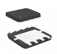
AT45DB081E Package
The following diagrams show the AT45DB081E Package.

Top View

Bottom View

Side View
AT45DB081E Manufacturer
Adesto Technologies provides application-specific and memory solutions optimized for the energy, data and security demands of IoT devices designed for the industrial, consumer, medical and communications markets. Adesto's Flagship memory family: DataFlash: Saves system energy, reduces board part count, saves microcontroller I/Os, widest operating voltage and power fail protection. Fusion: Designed for battery operated devices in the IoT space. Widest operating voltage and lowest standby current in the industry. Standard Flash: Lowest cost alternative, industry standard footprint and densities up to 128 Mb. Moneta: Industry's lowest power memory. Core voltage at 1.2 volts and 50 times lower power than competing data storage solutions.
Datasheet PDF
- Datasheets :
- PCN Assembly/Origin :
- PCN Design/Specification :
- Environmental Information :
How many pins of AT45DB081E-MHN-Y?
8 Pins.
What’s the operating temperature of AT45DB081E-MHN-Y?
-40°C~85°C TC.
What is the essential property of the AT45DB081E?
The AT45DB081E is a 1.7V minimum, serial-interface sequential access Flash memory ideally suited for a wide variety of digital voice, image, program code, and data storage applications.
 LT3750 Capacitor Charger Controller: Datasheet, Circuit, Equivalent
13 October 20212231
 AON7410 30V N-Channel MOSFET, AON7410 Equivalents
18 February 20224951
![1N4148WS-7-F Diode: Datasheet, Equivalent, Pinout [FAQ]](https://res.utmel.com/Images/Article/ba6694eb-7e58-4c6f-9508-4e03380f931a.jpg) 1N4148WS-7-F Diode: Datasheet, Equivalent, Pinout [FAQ]
1N4148WS-7-F Diode: Datasheet, Equivalent, Pinout [FAQ]24 April 20222824
 Top-Rated Suppliers of ADIS16209CCCZ Sensors
07 June 2025134
 KSZ9893R Gigabit Ethernet Switch: Pinout, Equivalent and Datasheet
17 February 20223305
 2N1711 NPN Power Transistor: 2N1711 Transistor Datasheet, Pinout and Equivalents
14 December 20215679
 A Comprehensive Guide to LTC6812HLWE-1#3ZZPBF Battery Management PMIC
06 March 2024189
 LM2904 Dual Op-Amp: Pinout, Features and Application
22 July 20214277
 Introduction to Step-down Transformers
14 October 20209276
 Getting Started with Arduino: What is Arduino and How to Use Arduino Boards
28 September 20236674
 Eight Internet of Things (IoT) Trends for 2022
08 April 20225303
 Types and Application of Position Sensors
31 October 20256758
 Tough Times for Japanese Component Manufacturers
10 August 20222892
 Lattice FPGA: The Ultimate Guide to Low-Power, Small Form Factor Solutions
19 September 20254595
 Solid State Relay Basics: Working, Features and Structure
17 September 20209705
 The Energy Internet - A New Era of Energy Management and Distribution
11 July 20235439
Adesto Technologies
In Stock: 30
Minimum: 1 Multiples: 1
Qty
Unit Price
Ext Price
1
$1.783755
$1.78
10
$1.682788
$16.83
100
$1.587536
$158.75
500
$1.497675
$748.84
1000
$1.412901
$1,412.90
Not the price you want? Send RFQ Now and we'll contact you ASAP.
Inquire for More Quantity
![AT25DF161-SH-T]() AT25DF161-SH-T
AT25DF161-SH-TAdesto Technologies
![AT25DF321A-SH-T]() AT25DF321A-SH-T
AT25DF321A-SH-TAdesto Technologies
![AT45DB321E-SHF-T]() AT45DB321E-SHF-T
AT45DB321E-SHF-TAdesto Technologies
![AT45DB041E-SSHN-T]() AT45DB041E-SSHN-T
AT45DB041E-SSHN-TAdesto Technologies
![AT45DB021E-SHN-T]() AT45DB021E-SHN-T
AT45DB021E-SHN-TAdesto Technologies
![AT45DB041E-SHN-T]() AT45DB041E-SHN-T
AT45DB041E-SHN-TAdesto Technologies
![AT45DB081E-SHN-T]() AT45DB081E-SHN-T
AT45DB081E-SHN-TAdesto Technologies
![AT25DF321A-MH-T]() AT25DF321A-MH-T
AT25DF321A-MH-TAdesto Technologies
![AT25SF041-SSHD-T]() AT25SF041-SSHD-T
AT25SF041-SSHD-TAdesto Technologies
![AT45DB641E-SHN-T]() AT45DB641E-SHN-T
AT45DB641E-SHN-TAdesto Technologies


