
 Product
 Brand
Brand Articles
 Tools
Tools
J111 JFET Transistor: J111 Datasheet, Pinout, Equivalent


JFET N-CH 35V 625MW TO92
J111 JFET N Channel Transistor is designed for low-level analogue switching, sample and hold circuits and chopper stabilized amplifiers. This article will unlock its datasheet, pinout, equivalent, application, and more detailed information about J111.

Construction and Working of JFET
J111 Pinout

J111 Pinout
J111 CAD Model
Symbol

J111 Symbol
Footprint

J111 Footprint
3D Model

J111 3D Model
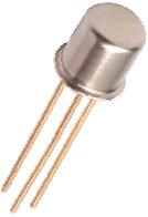
J111 Description
J111 is a silicon field-effect transistor with an N channel that is available in TO-92 and SOT-23 packages. J111 is a transistor in the J11x series, which also includes J112 and J113 transistors. All transistors in this series are designed primarily for analogue switching, current limiting, choppers, commentators, and sample and hold applications.
There are numerous advantages to incorporating these transistors in your design, including improved frequency response, high precision, reduced insertion loss, and low cost. Furthermore, the transistor has a low noise feature, allowing it to be employed in applications where the user has low noise requirements. The transistor also possesses symmetrical properties, which implies that the transistor's drain and source can be interchanged.
J111 Feature
TO-92 and SOT-23 packages are available.
N Channel JFET is a type of transistor (Symmetrical)
35V is the maximum drain-to-gate voltage.
–35V is the maximum reverse gate to source voltage.
50mA is the maximum continue gate current.
–5 to –3V is the maximum gate-to-source cutoff voltage.
625mW is the maximum power dissipation.
The maximum storage and operating temperatures should be between -55 and +150 °C.
J111 Application
Analog Switches
Choppers
Sample-and-Hold
Normally “On” Switches
Current Limiters
J111 Equivalent
How to Use J111?
As previously stated, the J111 FET or field-effect transistor is generally intended for current limiting, analogue switching, choppers, commentators, and sample and hold applications; nevertheless, the J111 transistor is a versatile device that may be utilized in a wide range of applications. The J111 is a good choice if you require a fast switching transistor with minimal leakage and capacitance.
How to Operate J111 in Safety?
It is usually suggested to check the absolute maximum ratings of the transistor before using it in your design or circuit, and we also propose that you do not utilize a component on its absolute maximum ratings, but rather remain at least 20% below them. As a result, the same holds true for the J111 transistor. Because the maximum drain to gate voltage is 35V, do not drive loads greater than 28V. Because the maximum continuous gate current is 50mA, do not drive a load more than 40mA and always store or operate the transistor at temperatures greater than -55°C and less than +150 °C.
J111 Package

J111 Package
J111 Manufacturer
ON Semiconductor (Nasdaq: ON) is driving energy efficient innovations, empowering customers to reduce global energy use. The company offers a comprehensive portfolio of energy-efficient power and signal management, logic, discrete and custom solutions to help design engineers solve their unique design challenges in automotive, communications, computing, consumer, industrial, LED lighting, medical, military/aerospace and power supply applications. ON Semiconductor operates a responsive, reliable, world-class supply chain and quality program, and a network of manufacturing facilities, sales offices and design centres in key markets throughout North America, Europe, and the Asia Pacific regions.
Specifications
- TypeParameter
- Lifecycle Status
Lifecycle Status refers to the current stage of an electronic component in its product life cycle, indicating whether it is active, obsolete, or transitioning between these states. An active status means the component is in production and available for purchase. An obsolete status indicates that the component is no longer being manufactured or supported, and manufacturers typically provide a limited time frame for support. Understanding the lifecycle status is crucial for design engineers to ensure continuity and reliability in their projects.
ACTIVE (Last Updated: 20 hours ago) - Factory Lead Time6 Weeks
- Mount
In electronic components, the term "Mount" typically refers to the method or process of physically attaching or fixing a component onto a circuit board or other electronic device. This can involve soldering, adhesive bonding, or other techniques to secure the component in place. The mounting process is crucial for ensuring proper electrical connections and mechanical stability within the electronic system. Different components may have specific mounting requirements based on their size, shape, and function, and manufacturers provide guidelines for proper mounting procedures to ensure optimal performance and reliability of the electronic device.
Through Hole - Mounting Type
The "Mounting Type" in electronic components refers to the method used to attach or connect a component to a circuit board or other substrate, such as through-hole, surface-mount, or panel mount.
Through Hole - Package / Case
refers to the protective housing that encases an electronic component, providing mechanical support, electrical connections, and thermal management.
TO-226-3, TO-92-3 (TO-226AA) - Number of Pins3
- Supplier Device Package
The parameter "Supplier Device Package" in electronic components refers to the physical packaging or housing of the component as provided by the supplier. It specifies the form factor, dimensions, and layout of the component, which are crucial for compatibility and integration into electronic circuits and systems. The supplier device package information typically includes details such as the package type (e.g., DIP, SOP, QFN), number of pins, pitch, and overall size, allowing engineers and designers to select the appropriate component for their specific application requirements. Understanding the supplier device package is essential for proper component selection, placement, and soldering during the manufacturing process to ensure optimal performance and reliability of the electronic system.
TO-92-3 - Weight201mg
- Manufacturer Package Identifier
The Manufacturer Package Identifier is a unique code or label assigned by the manufacturer to identify a specific package or housing style of an electronic component. This identifier helps in distinguishing between different package types of the same component, such as integrated circuits, transistors, or diodes. It typically includes information about the package dimensions, lead configuration, and other physical characteristics of the component. The Manufacturer Package Identifier is crucial for ensuring compatibility and proper assembly of electronic components in various devices and circuits.
TO-92 3L - Breakdown Voltage / V-35V
- Operating Temperature
The operating temperature is the range of ambient temperature within which a power supply, or any other electrical equipment, operate in. This ranges from a minimum operating temperature, to a peak or maximum operating temperature, outside which, the power supply may fail.
-55°C~150°C TJ - Packaging
Semiconductor package is a carrier / shell used to contain and cover one or more semiconductor components or integrated circuits. The material of the shell can be metal, plastic, glass or ceramic.
Bulk - Published2006
- Part Status
Parts can have many statuses as they progress through the configuration, analysis, review, and approval stages.
Active - Moisture Sensitivity Level (MSL)
Moisture Sensitivity Level (MSL) is a standardized rating that indicates the susceptibility of electronic components, particularly semiconductors, to moisture-induced damage during storage and the soldering process, defining the allowable exposure time to ambient conditions before they require special handling or baking to prevent failures
1 (Unlimited) - Termination
Termination in electronic components refers to the practice of matching the impedance of a circuit to prevent signal reflections and ensure maximum power transfer. It involves the use of resistors or other components at the end of transmission lines or connections. Proper termination is crucial in high-frequency applications to maintain signal integrity and reduce noise.
Through Hole - Max Operating Temperature
The Maximum Operating Temperature is the maximum body temperature at which the thermistor is designed to operate for extended periods of time with acceptable stability of its electrical characteristics.
150°C - Min Operating Temperature
The "Min Operating Temperature" parameter in electronic components refers to the lowest temperature at which the component is designed to operate effectively and reliably. This parameter is crucial for ensuring the proper functioning and longevity of the component, as operating below this temperature may lead to performance issues or even damage. Manufacturers specify the minimum operating temperature to provide guidance to users on the environmental conditions in which the component can safely operate. It is important to adhere to this parameter to prevent malfunctions and ensure the overall reliability of the electronic system.
-55°C - Voltage - Rated DC
Voltage - Rated DC is a parameter that specifies the maximum direct current (DC) voltage that an electronic component can safely handle without being damaged. This rating is crucial for ensuring the proper functioning and longevity of the component in a circuit. Exceeding the rated DC voltage can lead to overheating, breakdown, or even permanent damage to the component. It is important to carefully consider this parameter when designing or selecting components for a circuit to prevent any potential issues related to voltage overload.
35V - Max Power Dissipation
The maximum power that the MOSFET can dissipate continuously under the specified thermal conditions.
625mW - Current Rating
Current rating is the maximum current that a fuse will carry for an indefinite period without too much deterioration of the fuse element.
50mA - Base Part Number
The "Base Part Number" (BPN) in electronic components serves a similar purpose to the "Base Product Number." It refers to the primary identifier for a component that captures the essential characteristics shared by a group of similar components. The BPN provides a fundamental way to reference a family or series of components without specifying all the variations and specific details.
J111 - Element Configuration
The distribution of electrons of an atom or molecule (or other physical structure) in atomic or molecular orbitals.
Single - Power Dissipation
the process by which an electronic or electrical device produces heat (energy loss or waste) as an undesirable derivative of its primary action.
625mW - Power - Max
Power - Max is a parameter that specifies the maximum amount of power that an electronic component can handle without being damaged. It is typically measured in watts and indicates the upper limit of power that can be safely supplied to the component. Exceeding the maximum power rating can lead to overheating, malfunction, or permanent damage to the component. It is important to consider the power-max rating when designing circuits or systems to ensure proper operation and longevity of the electronic components.
625mW - FET Type
"FET Type" refers to the type of Field-Effect Transistor (FET) being used in an electronic component. FETs are three-terminal semiconductor devices that can be classified into different types based on their construction and operation. The main types of FETs include Metal-Oxide-Semiconductor FETs (MOSFETs), Junction FETs (JFETs), and Insulated-Gate Bipolar Transistors (IGBTs).Each type of FET has its own unique characteristics and applications. MOSFETs are commonly used in digital circuits due to their high input impedance and low power consumption. JFETs are often used in low-noise amplifiers and switching circuits. IGBTs combine the high input impedance of MOSFETs with the high current-carrying capability of bipolar transistors, making them suitable for high-power applications like motor control and power inverters.When selecting an electronic component, understanding the FET type is crucial as it determines the device's performance and suitability for a specific application. It is important to consider factors such as voltage ratings, current handling capabilities, switching speeds, and power dissipation when choosing the right FET type for a particular circuit design.
N-Channel - Drain to Source Voltage (Vdss)
The Drain to Source Voltage (Vdss) is a key parameter in electronic components, particularly in field-effect transistors (FETs) such as MOSFETs. It refers to the maximum voltage that can be applied between the drain and source terminals of the FET without causing damage to the component. Exceeding this voltage limit can lead to breakdown and potentially permanent damage to the device.Vdss is an important specification to consider when designing or selecting components for a circuit, as it determines the operating range and reliability of the FET. It is crucial to ensure that the Vdss rating of the component is higher than the maximum voltage expected in the circuit to prevent failures and ensure proper functionality.In summary, the Drain to Source Voltage (Vdss) is a critical parameter that defines the maximum voltage tolerance of a FET component and plays a significant role in determining the overall performance and reliability of electronic circuits.
35V - Continuous Drain Current (ID)
Continuous Drain Current (ID) is a key parameter in electronic components, particularly in field-effect transistors (FETs) such as MOSFETs. It refers to the maximum current that can flow continuously through the drain terminal of the FET without causing damage to the component. This parameter is crucial for determining the power handling capability of the FET and is specified by the manufacturer in the component's datasheet. Designers must ensure that the actual operating current does not exceed the specified Continuous Drain Current to prevent overheating and potential failure of the component.
20mA - Gate to Source Voltage (Vgs)
The Gate to Source Voltage (Vgs) is a crucial parameter in electronic components, particularly in field-effect transistors (FETs) such as MOSFETs. It refers to the voltage difference between the gate and source terminals of the FET. This voltage determines the conductivity of the FET and controls the flow of current through the device. By varying the Vgs, the FET can be switched on or off, allowing for precise control of electronic circuits. Understanding and properly managing the Vgs is essential for ensuring the reliable and efficient operation of FET-based circuits.
-35V - Drain to Source Resistance
The Drain to Source Resistance, often denoted as RDS(on), is a crucial parameter in electronic components, particularly in field-effect transistors (FETs) such as MOSFETs. It represents the resistance between the drain and source terminals when the FET is in its on-state, conducting current. A lower RDS(on) value indicates better conductivity and efficiency, as it results in less power dissipation and heat generation in the component. Designers often aim to minimize RDS(on) to improve the performance and overall efficiency of electronic circuits, especially in power applications where minimizing losses is critical.
30Ohm - Current - Drain (Idss) @ Vds (Vgs=0)
The parameter "Current - Drain (Idss) @ Vds (Vgs=0)" in electronic components refers to the maximum drain current that flows through the device when the gate-source voltage (Vgs) is zero. This parameter is typically specified for field-effect transistors (FETs) and is an important characteristic that indicates the device's maximum current-carrying capacity in the off state. It helps in determining the saturation current of the FET and is crucial for designing circuits where high current handling capability is required. Manufacturers provide this parameter in the datasheet of the component to assist engineers and designers in selecting the appropriate component for their applications.
20mA @ 15V - Voltage - Cutoff (VGS off) @ Id
Voltage - Cutoff (VGS off) @ Id refers to the gate-source voltage at which a field-effect transistor (FET) or similar device ceases to conduct, effectively turning it off. This parameter indicates the threshold voltage that separates the conducting state from the cutoff state for a specified drain current (Id). It is crucial for determining the operating characteristics of the device in various applications, ensuring efficient switching and control in electronic circuits.
3V @ 1μA - Voltage - Breakdown (V(BR)GSS)
Voltage - Breakdown (V(BR)GSS) is a parameter used to describe the maximum gate-source voltage that can be applied to a field-effect transistor (FET) without causing a breakdown in the gate-source junction. This parameter is crucial in determining the safe operating limits of the FET and helps prevent damage to the component. When the gate-source voltage exceeds the breakdown voltage, it can lead to a sudden increase in current flow and potentially damage the FET. Therefore, understanding and adhering to the specified V(BR)GSS value is essential for proper functioning and reliability of electronic circuits utilizing FETs.
35V - Resistance - RDS(On)
Resistance - RDS(On) refers to the on-state resistance of a MOSFET when it is fully turned on. It is a critical parameter that indicates the resistance between the drain and source terminals of the device in the conducting state. Lower RDS(On) values result in reduced power loss and heat generation during operation, making it an important specification for efficiency in electronic circuits. It is typically measured in ohms and is a key consideration in the selection of transistors for power applications.
30Ohms - Height5.33mm
- Length5.2mm
- Width4.19mm
- REACH SVHC
The parameter "REACH SVHC" in electronic components refers to the compliance with the Registration, Evaluation, Authorization, and Restriction of Chemicals (REACH) regulation regarding Substances of Very High Concern (SVHC). SVHCs are substances that may have serious effects on human health or the environment, and their use is regulated under REACH to ensure their safe handling and minimize their impact.Manufacturers of electronic components need to declare if their products contain any SVHCs above a certain threshold concentration and provide information on the safe use of these substances. This information allows customers to make informed decisions about the potential risks associated with using the components and take appropriate measures to mitigate any hazards.Ensuring compliance with REACH SVHC requirements is essential for electronics manufacturers to meet regulatory standards, protect human health and the environment, and maintain transparency in their supply chain. It also demonstrates a commitment to sustainability and responsible manufacturing practices in the electronics industry.
No SVHC - Radiation Hardening
Radiation hardening is the process of making electronic components and circuits resistant to damage or malfunction caused by high levels of ionizing radiation, especially for environments in outer space (especially beyond the low Earth orbit), around nuclear reactors and particle accelerators, or during nuclear accidents or nuclear warfare.
No - RoHS Status
RoHS means “Restriction of Certain Hazardous Substances” in the “Hazardous Substances Directive” in electrical and electronic equipment.
ROHS3 Compliant - Lead Free
Lead Free is a term used to describe electronic components that do not contain lead as part of their composition. Lead is a toxic material that can have harmful effects on human health and the environment, so the electronics industry has been moving towards lead-free components to reduce these risks. Lead-free components are typically made using alternative materials such as silver, copper, and tin. Manufacturers must comply with regulations such as the Restriction of Hazardous Substances (RoHS) directive to ensure that their products are lead-free and environmentally friendly.
Lead Free
Parts with Similar Specs
- ImagePart NumberManufacturerMountPackage / CaseDrain to Source Voltage (Vdss)Continuous Drain Current (ID)Drain to Source ResistanceMax Power DissipationPower DissipationGate to Source Voltage (Vgs)View Compare
![J111]()
J111
Through Hole
TO-226-3, TO-92-3 (TO-226AA)
35 V
20 mA
30 Ω
625 mW
625 mW
-35 V
![J112-D27Z]()
Through Hole
TO-226-3, TO-92-3 (TO-226AA) (Formed Leads)
35 V
5 mA
50 Ω
625 mW
625 mW
-35 V
![PN4091]()
Through Hole
TO-226-3, TO-92-3 (TO-226AA)
35 V
2 mA
100 Ω
625 mW
625 mW
-35 V
![J113]()
Through Hole
TO-226-3, TO-92-3 (TO-226AA)
40 V
50 mA
30 Ω
625 mW
625 mW
-40 V


Datasheet PDF
- Datasheets :
- PCN Assembly/Origin :
- PCN Packaging :
- Environmental Information :
- ReachStatement :
- PCN Design/Specification :
What channel does J111 have?
J111 is a silicon field-effect transistor with an N channel.
What types of transistors are included in the J11x series?
J111, J112 and J113.
What feature does J111 have?
Low noise feature.
How much below the absolute maximum ratings of the J111 transistor?
20%.
What type of transistor does the same hold true for?
J111.
![ATTINY84A-PU AVR series Microcontroller IC 8-Bit 20MHz[FAQ]: Datasheet, Features, and Pinout](https://res.utmel.com/Images/Article/889533d0-63dd-4ec6-8d21-6b346255db18.jpg) ATTINY84A-PU AVR series Microcontroller IC 8-Bit 20MHz[FAQ]: Datasheet, Features, and Pinout
ATTINY84A-PU AVR series Microcontroller IC 8-Bit 20MHz[FAQ]: Datasheet, Features, and Pinout18 March 2022736
 LM2902 Op-Amp: Where & How to Use LM2902?
04 December 20216172
 SX1276 Transceiver: Datasheet, SX1276 vs. SX1272
09 November 202117072
 BNO080 Sensor: Datasheet, Pinout and Circuit
05 August 20216606
 2N2907A Bipolar Transistor PNP TO-18: Datasheet, Pinout, and Equivalents
09 February 20222474
 LM386 Low Voltage Audio Power Amplifier: Features, Specifications, Applications
10 May 20212195
 TDA7293 DMOS Audio Amplifier: Datasheet, TDA7293 vs. TDA7294
03 December 202116826
 OPA1656 Audio Op Amps: Datasheet, Pinout and Applications
11 October 202112328
 US Energy Department Funds Next-Gen Semiconductor Projects to Improve Power Grids
09 December 20234027
 Semiconductor Veteran Kevin Conley Takes Helm as CEO of Applied Brain Research
13 September 20233709
 2026 Advanced Packaging Components Trends: Navigating Shortages and Ecosystem Impacts
20 July 2026422
 Introduction to TRIAC and TRIAC Dimmer
10 September 202010438
 Three-Phase WBG Resonant Converter Integrated with PCB Winding Transformer
20 October 20232619
 Everything You Need to Know About Fuse Resistors
30 July 20253968
 Arduino Based Gas Leakage Detection
29 August 20239477
 What is CPLD (Complex Programmable Logic Device)?
15 October 202512085
ON Semiconductor
In Stock: 6145
United States
China
Canada
Japan
Russia
Germany
United Kingdom
Singapore
Italy
Hong Kong(China)
Taiwan(China)
France
Korea
Mexico
Netherlands
Malaysia
Austria
Spain
Switzerland
Poland
Thailand
Vietnam
India
United Arab Emirates
Afghanistan
Åland Islands
Albania
Algeria
American Samoa
Andorra
Angola
Anguilla
Antigua & Barbuda
Argentina
Armenia
Aruba
Australia
Azerbaijan
Bahamas
Bahrain
Bangladesh
Barbados
Belarus
Belgium
Belize
Benin
Bermuda
Bhutan
Bolivia
Bonaire, Sint Eustatius and Saba
Bosnia & Herzegovina
Botswana
Brazil
British Indian Ocean Territory
British Virgin Islands
Brunei
Bulgaria
Burkina Faso
Burundi
Cabo Verde
Cambodia
Cameroon
Cayman Islands
Central African Republic
Chad
Chile
Christmas Island
Cocos (Keeling) Islands
Colombia
Comoros
Congo
Congo (DRC)
Cook Islands
Costa Rica
Côte d’Ivoire
Croatia
Cuba
Curaçao
Cyprus
Czechia
Denmark
Djibouti
Dominica
Dominican Republic
Ecuador
Egypt
El Salvador
Equatorial Guinea
Eritrea
Estonia
Eswatini
Ethiopia
Falkland Islands
Faroe Islands
Fiji
Finland
French Guiana
French Polynesia
Gabon
Gambia
Georgia
Ghana
Gibraltar
Greece
Greenland
Grenada
Guadeloupe
Guam
Guatemala
Guernsey
Guinea
Guinea-Bissau
Guyana
Haiti
Honduras
Hungary
Iceland
Indonesia
Iran
Iraq
Ireland
Isle of Man
Israel
Jamaica
Jersey
Jordan
Kazakhstan
Kenya
Kiribati
Kosovo
Kuwait
Kyrgyzstan
Laos
Latvia
Lebanon
Lesotho
Liberia
Libya
Liechtenstein
Lithuania
Luxembourg
Macao(China)
Madagascar
Malawi
Maldives
Mali
Malta
Marshall Islands
Martinique
Mauritania
Mauritius
Mayotte
Micronesia
Moldova
Monaco
Mongolia
Montenegro
Montserrat
Morocco
Mozambique
Myanmar
Namibia
Nauru
Nepal
New Caledonia
New Zealand
Nicaragua
Niger
Nigeria
Niue
Norfolk Island
North Korea
North Macedonia
Northern Mariana Islands
Norway
Oman
Pakistan
Palau
Palestinian Authority
Panama
Papua New Guinea
Paraguay
Peru
Philippines
Pitcairn Islands
Portugal
Puerto Rico
Qatar
Réunion
Romania
Rwanda
Samoa
San Marino
São Tomé & Príncipe
Saudi Arabia
Senegal
Serbia
Seychelles
Sierra Leone
Sint Maarten
Slovakia
Slovenia
Solomon Islands
Somalia
South Africa
South Sudan
Sri Lanka
St Helena, Ascension, Tristan da Cunha
St. Barthélemy
St. Kitts & Nevis
St. Lucia
St. Martin
St. Pierre & Miquelon
St. Vincent & Grenadines
Sudan
Suriname
Svalbard & Jan Mayen
Sweden
Syria
Tajikistan
Tanzania
Timor-Leste
Togo
Tokelau
Tonga
Trinidad & Tobago
Tunisia
Turkey
Turkmenistan
Turks & Caicos Islands
Tuvalu
U.S. Outlying Islands
U.S. Virgin Islands
Uganda
Ukraine
Uruguay
Uzbekistan
Vanuatu
Vatican City
Venezuela
Wallis & Futuna
Yemen
Zambia
Zimbabwe
![MMBFJ177LT1G]() MMBFJ177LT1G
MMBFJ177LT1GON Semiconductor
![MMBFJ201]() MMBFJ201
MMBFJ201ON Semiconductor
![MMBFJ108]() MMBFJ108
MMBFJ108ON Semiconductor
![MMBF4391LT1G]() MMBF4391LT1G
MMBF4391LT1GON Semiconductor
![MMBF4393LT1G]() MMBF4393LT1G
MMBF4393LT1GON Semiconductor
![MMBFJ175]() MMBFJ175
MMBFJ175ON Semiconductor
![MMBFJ175LT1G]() MMBFJ175LT1G
MMBFJ175LT1GON Semiconductor
![MMBF4392LT1G]() MMBF4392LT1G
MMBF4392LT1GON Semiconductor
![MMBFJ202]() MMBFJ202
MMBFJ202ON Semiconductor
![J175-D26Z]() J175-D26Z
J175-D26ZON Semiconductor


